256 Kb (64K x 4) Static RAM
CY7C194B
CY7C195B
Cypress Semiconductor Corporation
·
3901 North First Street
·
San Jose
,
CA 95134
·
408-943-2600
Document #: 38-05409 Rev. *A
Revised September 17, 2003
Features
· Fast access time: 12 ns, 15 ns, and 25 ns
· Wide voltage range: 5.0V ± 10% (4.5V to 5.5V)
· CMOS for optimum speed/power
· TTL-compatible inputs and outputs
· Available in 24 DIP, 24 SOJ, 28 DIP, and 28 SOJ
General Description
1
The CY7C194B-CY7C195B is a high-performance CMOS
Asynchronous SRAM organized as 64K × 4 bits that supports
an asynchronous memory interface. The device features an
automatic power-down feature that significantly reduces
power consumption when deselected. Output enable (OE) is
supported only in CY7C195B.
2
See the Truth Table in this data sheet for a complete
description of read and write modes.
The CY7C194B-CY7C195B is available in 24 DIP, 24 SOJ, 28
DIP, and 28 SOJ package(s).
Notes:
Notes:
1. For best-practice recommendations, please refer to the Cypress application note System Design Guidelines on www.cypress.com.
2. All OE-specific descriptions and parameters in this datasheet pertain to CY7C195 only.
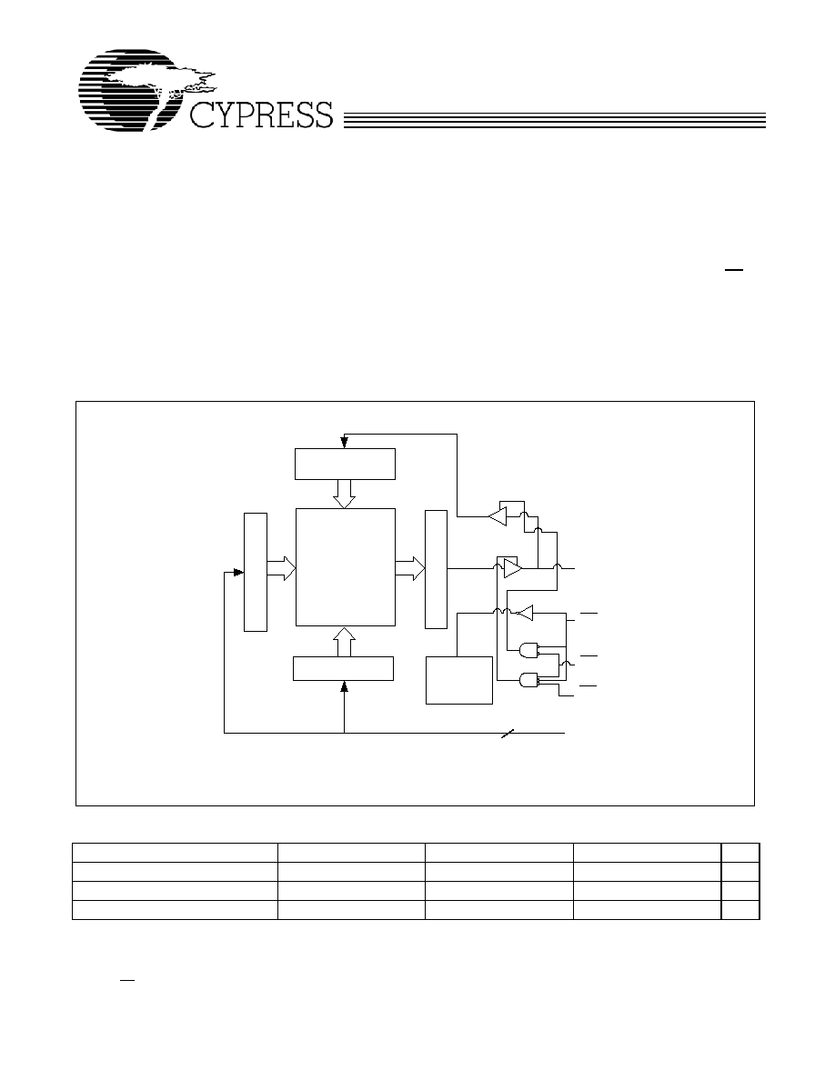
Row
D
eco
d
er
RAM Array
Column Decoder
Input Buffer
Se
n
s
e
A
mps
A
X
Power
Down
Circuit
I/Ox
OE
WE
CE
X
(7C195 only)
Logic Block Diagram
Product Portfolio
12 ns
15 ns
25 ns
Unit
Maximum Access Time
12
15
25
ns
Maximum Operating Current
90
80
80
mA
Maximum CMOS Standby Current
10
10
10
mA
CY7C194B
CY7C195B
Document #: 38-05409 Rev. *A
Page 2 of 13
Pin Layout and Specifications
NC
A
6
A
7
A
8
A
9
A
10
A
11
A
12
A
13
A
14
A
15
CE
OE
GND
WE
I/O
0
I/O
1
I/O
2
I/O
3
NC
NC
A
0
A
1
A
2
A
3
A
4
A
5
V
CC
1
2
3
4
5
6
7
8
9
10
11
12
13
14
15
16
17
18
19
20
21
22
23
24
25
26
27
28
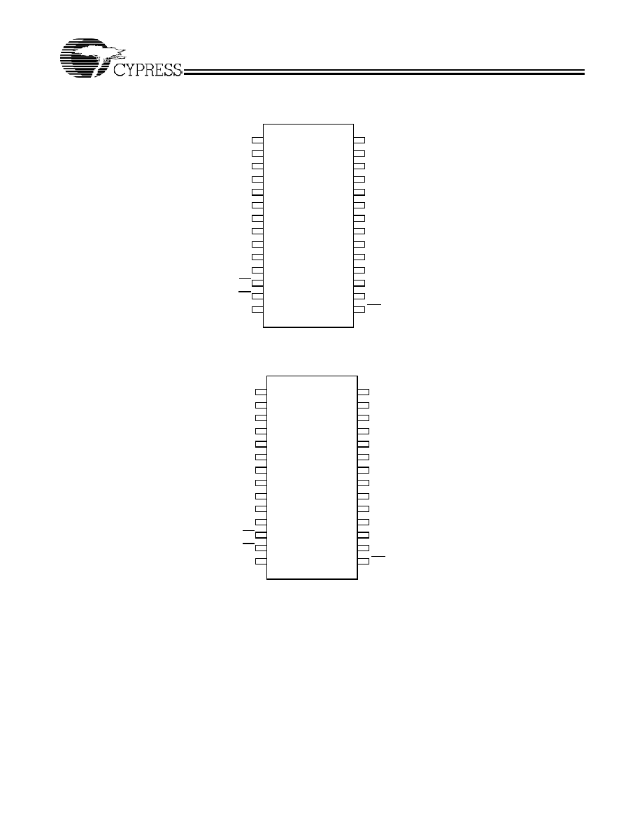
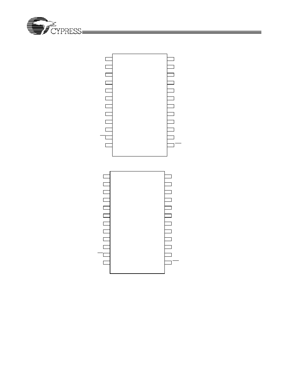
CY7C195B 28 DIP (6.9 × 35.6 × 3.5 mm) P21
NC
A
6
A
7
A
8
A
9
A
10
A
11
A
12
A
13
A
14
A
15
CE
OE
GND
WE
I/O
0
I/O
1
I/O
2
I/O
3
NC
NC
A
0
A
1
A
2
A
3
A
4
A
5
V
CC
1
2
3
4
5
6
7
8
9
10
11
12
13
14
15
16
17
18
19
20
21
22
23
24
25
26
27
28
CY7C195B 28 SOJ (8 × 18 × 3.5 mm) V21
CY7C194B
CY7C195B
Document #: 38-05409 Rev. *A
Page 3 of 13
Pin Layout and Specifications
(continued)
A
6
A
7
A
8
A
9
A
10
A
11
A
12
A
13
A
14
A
15
CE
GND
WE
I/O
0
I/O
1
I/O
2
I/O
3
A
0
A
1
A
2
A
3
A
4
A
5
V
CC
1
2
3
4
5
6
7
8
9
10
11
12
13
14
15
16
17
18
19
20
21
22
23
24
CY7C194B 24 SOJ (8 × 15 × 3.5 mm) V13
A
6
A
7
A
8
A
9
A
10
A
11
A
12
A
13
A
14
A
15
CE
GND
WE
I/O
0
I/O
1
I/O
2
I/O
3
A
0
A
1
A
2
A
3
A
4
A
5
V
CC
1
2
3
4
5
6
7
8
9
10
11
12
13
14
15
16
17
18
19
20
21
22
23
24
CY7C194B 24 DIP (6.6 × 31.8 × 3.5 mm) P13
CY7C194B
CY7C195B
Document #: 38-05409 Rev. *A
Page 4 of 13
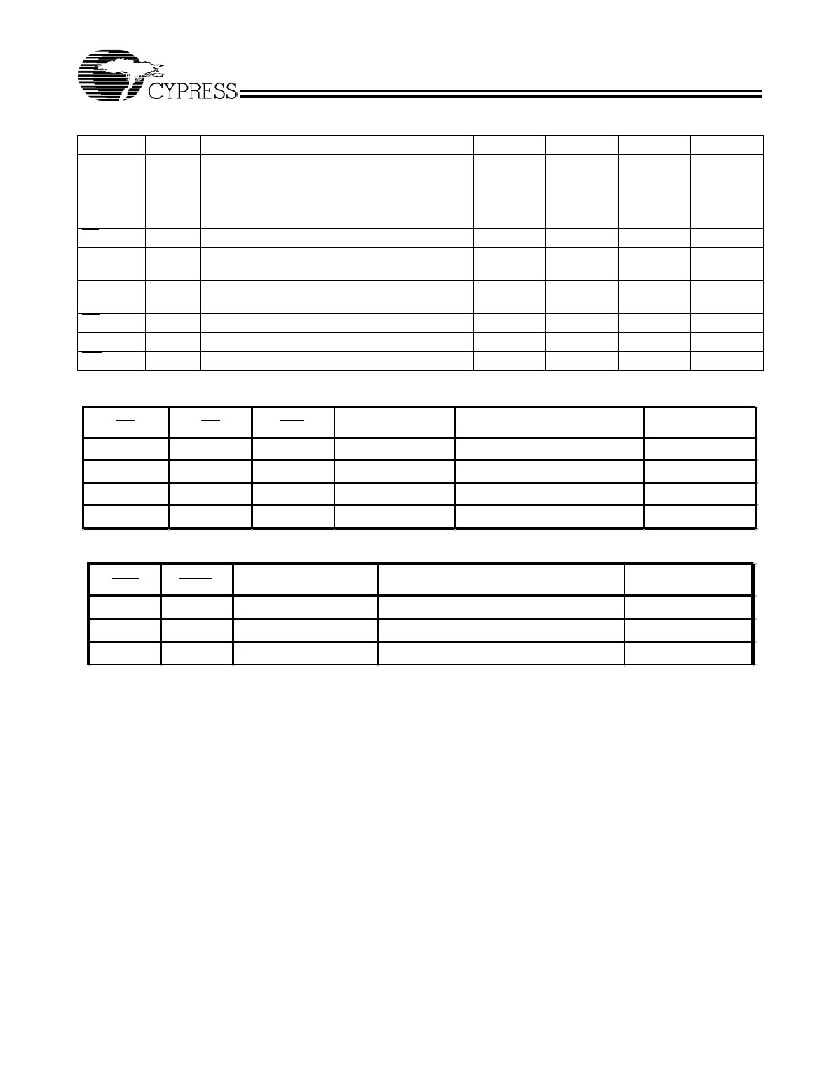
CY7C195B Truth Table
CY7C194B Truth Table
Pin Description
Pin
Type
Description
28 DIP
24 DIP
24 SOJ
28 SOJ
A
X
Input
Address Inputs.
2, 3, 4, 5, 6,
7, 8, 9, 10,
11, 22, 23,
24, 25, 26,
27
1, 2, 3, 4, 5,
6, 7, 8, 9,
10, 18, 19,
20, 21, 22,
23
1, 2, 3, 4, 5,
6, 7, 8, 9,
10, 18, 19,
20, 21, 22,
23
2, 3, 4, 5, 6,
7, 8, 9, 10,
11, 22, 23,
24, 25, 26,
27
CE
Control
Chip Enable.
12
11
11
12
I/O
X
Input or
Output
Data Input/Outputs.
16, 17, 18,
19
14, 15, 16,
17
14, 15, 16,
17
16, 17, 18,
19
NC
No Connect. Pins are not internally connected to
the die.
1, 20, 21
1, 20, 21
OE
Control
Output Enable (CY7C195 only).
13
13
V
CC
Supply
Power (5.0V).
28
24
24
28
WE
Control
Write Enable.
15
13
13
15
CE
OE
WE
I/Ox
Mode
Power
H
X
X
High Z
Deselect / Power-Down
Standby (I
SB
)
L
L
H
Data Out
Read
Active (I
CC
)
L
X
L
Data In
Write
Active (I
CC
)
L
H
H
High Z
Selected, outputs disabled
Active (I
CC
)
CE
WE
Input/Output
Mode
Power
H
X
High Z
Power-Down
Standby (I
SB
)
L
H
Data Out
Read
Active (I
CC
)
L
L
Data In
Write
Active (I
CC
)
CY7C194B
CY7C195B
Document #: 38-05409 Rev. *A
Page 5 of 13
Maximum Ratings
(Above which the useful life may be impaired. For user guidelines, not tested.)
Operating Range
DC Electrical Characteristics
3
Capacitance
4
Parameter
Description
Value
Unit
T
STG
Storage Temperature
65 to +150
°C
T
AMB
Ambient Temperature with Power Applied (i.e. case temperature)
55 to +125
°C
V
CC
Core Supply Voltage Relative to V
SS
0.5 to +7.0
V
V
CC
DC Voltage Applied to any Pin Relative to V
SS
0.5 to V
CC
+ null
V
I
OUT
Output Short-Circuit Current
20
mA
V
ESD
Static Discharge Voltage (per MIL-STD-883, Method 3015)
> 2001
V
I
LU
Latch-up Current
> 200
mA
Range
Ambient Temperature (T
A
)
Voltage Range (V
CC
)
Commercial
0°C to 70°C
5.0V ± 10%
Parameter
Description
Condition
12 ns
15 ns
25 ns
Unit
Min
Max
Min
Max
Min
Max
V
IH
Input HIGH Volt-
age
2.2
V
CC
+
0.3
2.2
V
CC
+
0.3
2.2
V
CC
+
0.3
V
V
IL
Input LOW Volt-
age
0.3
0.8
0.3
0.8
0.5
0.8
V
V
OH
Output HIGH Volt-
age
V
CC
= Min., loh = -4.0 ma
2.4
2.4
2.4
V
V
OL
Output LOW Volt-
age
V
CC
= Min., lol = 8.0 ma
0.4
0.4
0.4
V
I
CC
V
CC
Operating
Supply Current
V
CC
= Max., I
OUT
= 0 mA, f =
F
MAX
= 1 / t
RC
90
80
80
mA
I
SB1
Automatic CE
Power-down Cur-
rent TTL Inputs
V
CC
= Max., CE
V
IH
, V
IN
V
IH
or V
IN
V
IL
, f = F
MAX
30
30
30
mA
I
SB2
Automatic CE
Power-down Cur-
rent CMOS Inputs
V
CC
= Max., CE
V
CC
- 0.3v,
V
IN
> V
CC
- 0.3v or V
IN
0.3,f
= 0 Commercial
10
10
10
mA
I
OZ
Output Leakage
Current
GND
Vi V
CC
, Output Dis-
abled
5
+5
5
+5
5
+5
uA
I
IX
Input Load Cur-
rent
GND
Vi V
CC
5
+5
5
+5
5
+5
uA
Notes:
3. V
IL
(min) = 2.0V for pulse durations of less than 20 ns.
Parameter
Description
Conditions
Max
Unit
ALL - PACKAGES
C
IN
Input Capacitance
T
A
= 25C, f = 1 MHz,
V
CC
= 5.0V
7
pF
C
OUT
Output Capacitance
10
4. Tested initially and after any design or process change that may affect these parameters.