9-Mb (256K x 32) Pipelined DCD Sync SRAM
CY7C1368B
Cypress Semiconductor Corporation
·
3901 North First Street
·
San Jose
,
CA 95134
·
408-943-2600
Document #: 38-05419 Rev. **
Revised December 23, 2003
Features
· Registered inputs and outputs for pipelined operation
· Optimal for performance (Double-Cycle deselect)
-- Depth expansion without wait state
· 256K × 32-bit common I/O architecture
· 3.3V 5% and +10% core power supply (V
DD
)
· 3.3V I/O supply (V
DDQ
)
· Fast clock-to-output times
-- 3.0 ns (for 200-MHz device)
-- 3.5 ns (for 166-MHz device)
· Provide high-performance 3-1-1-1 access rate
· User-selectable burst counter supporting Intel
Pentium
interleaved or linear burst sequences
· Multiple chip enables for depth expansion: three chip
enables for A package version and two chip enables for
AJ package version
· Separate processor and controller address strobes
· Synchronous self-timed writes
· Asynchronous Output Enable
· JEDEC-standard 100-pin TQFP package and pinout
· "ZZ" Sleep Mode option
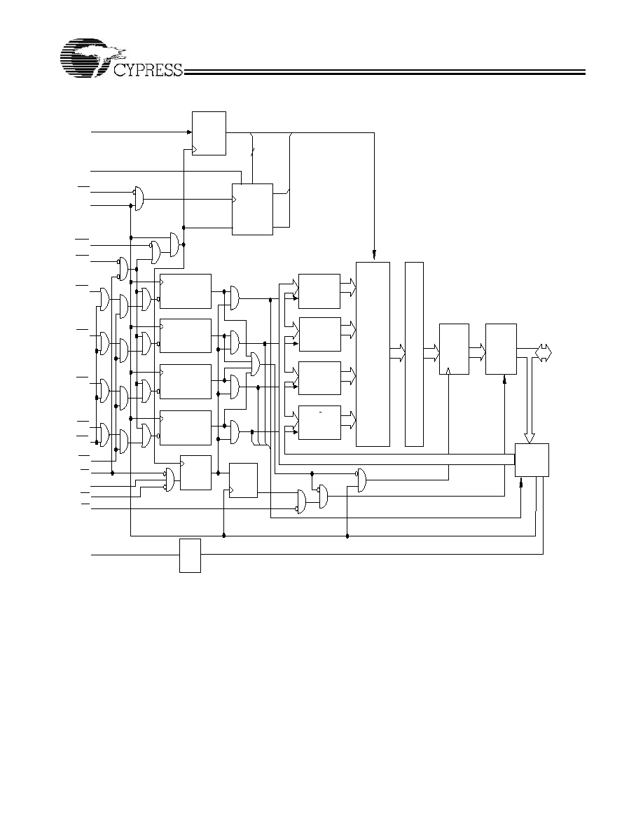
Functional Description
[1]
The CY7C1368B SRAM integrates 262,144 x 32 SRAM cells
with advanced synchronous peripheral circuitry and a two-bit
counter for internal burst operation. All synchronous inputs are
gated by registers controlled by a positive-edge-triggered
Clock Input (CLK). The synchronous inputs include all
addresses, all data inputs, address-pipelining Chip Enable
(CE
1
), depth-expansion Chip Enables (CE
2
and
CE
3
[2]
), Burst
Control inputs (ADSC, ADSP, and ADV), Write Enables (BW
A
,
BW
B
, BW
C
, BW
D
and BWE), and Global Write (GW).
Asynchronous inputs include the Output Enable (OE) and the
ZZ pin.
Addresses and chip enables are registered at rising edge of
clock when either Address Strobe Processor (ADSP) or
Address Strobe Controller (ADSC) are active. Subsequent
burst addresses can be internally generated as controlled by
the Advance pin (ADV).
Address, data inputs, and write controls are registered on-chip
to initiate a self-timed Write cycle. This part supports Byte
Write operations (see Pin Descriptions and Truth Table for
further details). Write cycles can be one to four bytes wide as
controlled by the byte write control inputs. GW active LOW
causes all bytes to be written. This device incorporates an
additional pipelined enable register which delays turning off
the output buffers an additional cycle when a deselect is
executed.This feature allows depth expansion without penal-
izing system performance.
The CY7C1368B operates from a +3.3V core power supply
and a +3.3V supply for the I/Os. All inputs and outputs are
JEDEC-standard JESD8-5-compatible.
Notes:
1. For best-practice recommendations, please refer to the Cypress application note "System Design Guidelines" on http://www.cypress.com.
2. CE
3
is for A version (3 Chip enable option) only
Selection Guide
200 MHz
166 MHz
Unit
Maximum Access Time
3.0
3.5
ns
Maximum Operating Current
220
180
mA
Maximum CMOS Standby Current
30
30
mA
CY7C1368B
Document #: 38-05419 Rev. **
Page 5 of 17
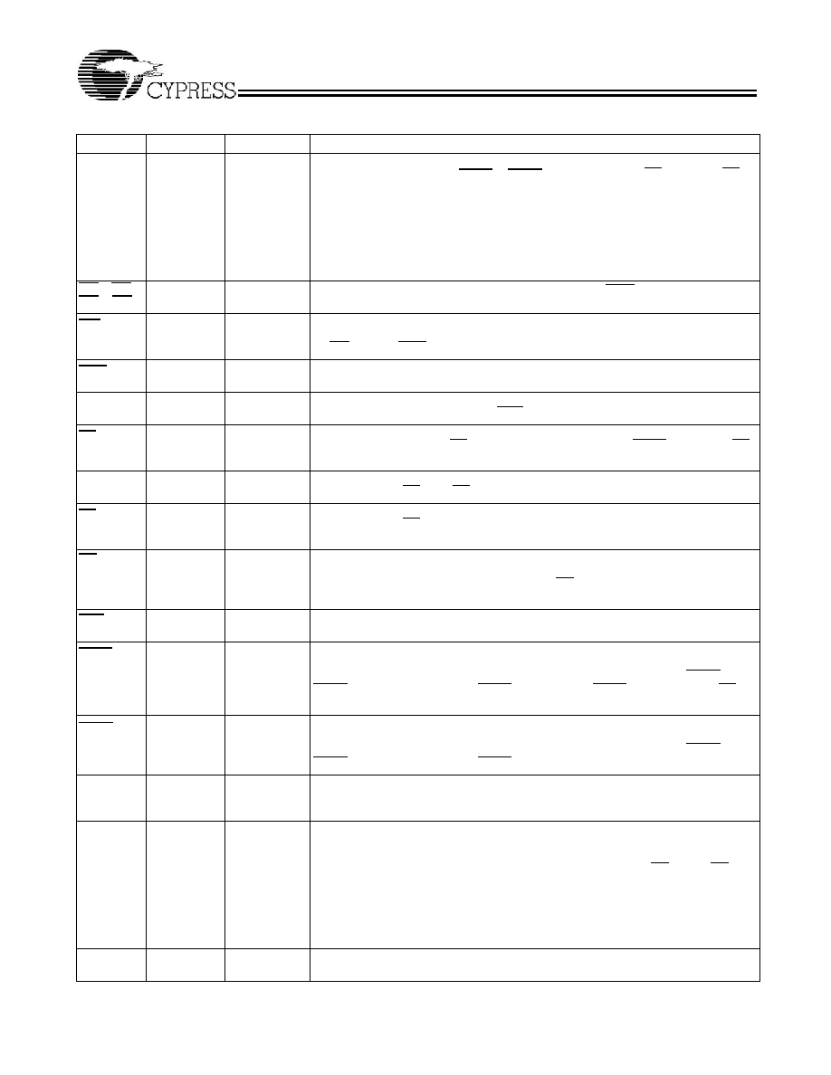
Pin Descriptions
Pin
TQFP
Type
Description
A
0
, A
1
, A
37, 36,
32,33,34,
35,44,45,
46,47,48,
49,50,80,
81,82,99,
100, 92
(AJC), 43
(AC)
Input-
Synchronous
Address Inputs used to select one of the 256K address locations. Sampled at
the rising edge of the CLK if ADSP or ADSC is active LOW, and CE
1
,
CE
2
, and
CE
3
[1]
are sampled active. A
[1:0]
are fed to the two-bit counter.
BW
A
, BW
B
,
BW
C
, BW
D
93,94
Input-
Synchronous
Byte Write Select Inputs, active LOW. Qualified with BWE to conduct byte writes
to the SRAM. Sampled on the rising edge of CLK.
GW
88
Input-
Synchronous
Global Write Enable Input, active LOW. When asserted LOW on the rising edge
of CLK, a global write is conducted (ALL bytes are written, regardless of the values
on BW
[A:D]
and BWE).
BWE
87
Input-
Synchronous
Byte Write Enable Input, active LOW. Sampled on the rising edge of CLK. This
signal must be asserted LOW to conduct a byte write.
CLK
89
Input-
Clock
Clock Input. Used to capture all synchronous inputs to the device. Also used to
increment the burst counter when ADV is asserted LOW, during a burst operation.
CE
1
98
Input-
Synchronous
Chip Enable 1 Input, active LOW. Sampled on the rising edge of CLK. Used in
conjunction with CE
2
and CE
3
to select/deselect the device. ADSP is ignored if CE
1
is HIGH.
CE
2
97
Input-
Synchronous
Chip Enable 2 Input, active HIGH. Sampled on the rising edge of CLK. Used in
conjunction with CE
1
and CE
3
to select/deselect the device.
CE
3
[2]
92
Input-
Synchronous
Chip Enable 3 Input, active LOW. Sampled on the rising edge of CLK. Used in
conjunction with CE
1
and
CE
2
to select/deselect the device. Not available for AJ
package version.
OE
86
Input-
Asynchronous
Output Enable, asynchronous input, active LOW. Controls the direction of the
I/O pins. When LOW, the I/O pins behave as outputs. When deasserted HIGH, I/O
pins are tri-stated, and act as input data pins. OE is masked during the first clock of
a read cycle when emerging from a deselected state.
ADV
83
Input-
Synchronous
Advance Input signal, sampled on the rising edge of CLK, active LOW. When
asserted, it automatically increments the address in a burst cycle.
ADSP
84
Input-
Synchronous
Address Strobe from Processor, sampled on the rising edge of CLK, active
LOW. When asserted LOW, addresses presented to the device are captured in the
address registers. A
[1:0]
are also loaded into the burst counter. When ADSP and
ADSC are both asserted, only ADSP is recognized. ASDP is ignored when CE
1
is
deasserted HIGH.
ADSC
85
Input-
Synchronous
Address Strobe from Controller, sampled on the rising edge of CLK, active
LOW. When asserted LOW, addresses presented to the device are captured in the
address registers. A
[1:0]
are also loaded into the burst counter. When ADSP and
ADSC are both asserted, only ADSP is recognized.
ZZ
64
Input-
Asynchronous
ZZ "sleep" Input, active HIGH. When asserted HIGH places the device in a
non-time-critical "sleep" condition with data integrity preserved. For normal
operation, this pin has to be LOW or left floating. ZZ pin has an internal pull-down.
DQs
2,3,
6,7,8,9,12,13
,18,19,22,23,
24,25,28,29,
52,53,56,57,
58,59,62,63,
68,69,72,73,
74,75.75,78,
79
I/O-
Synchronous
Bidirectional Data I/O lines. As inputs, they feed into an on-chip data register that
is triggered by the rising edge of CLK. As outputs, they deliver the data contained in
the memory location specified by the addresses presented during the previous clock
rise of the read cycle. The direction of the pins is controlled by OE. When OE is
asserted LOW, the pins behave as outputs. When HIGH, DQs are placed in a tri-state
condition.
V
DD
15,41,65,
91
Power Supply Power supply inputs to the core of the device.