4-Mb (128K x 36) Pipelined SRAM with NoblTM Architecture
CY7C1350F
Cypress Semiconductor Corporation
·
3901 North First Street
·
San Jose
,
CA 95134
·
408-943-2600
Document #: 38-05305 Rev. *A
Revised January 19, 2004
1CY7C1350F
Features
· Pin compatible and functionally equivalent to ZBTTM
devices
· Internally self-timed output buffer control to eliminate
the need to use OE
· Byte Write capability
· 128K x 36 common I/O architecture
· Single 3.3V power supply
· 2.5V/3.3V I/O Operation
· Fast clock-to-output times
-- 2.6 ns (for 250-MHz device)
-- 2.6 ns (for 225-MHz device)
-- 2.8 ns (for 200-MHz device)
-- 3.5 ns (for 166-MHz device)
-- 4.0 ns (for 133-MHz device)
-- 4.5 ns (for 100-MHz device)
· Clock Enable (CEN) pin to suspend operation
· Synchronous self-timed writes
· Asynchronous output enable (OE)
· JEDEC-standard 100 TQFP and 119 BGA packages
· Burst Capability--linear or interleaved burst order
· "ZZ" Sleep mode option
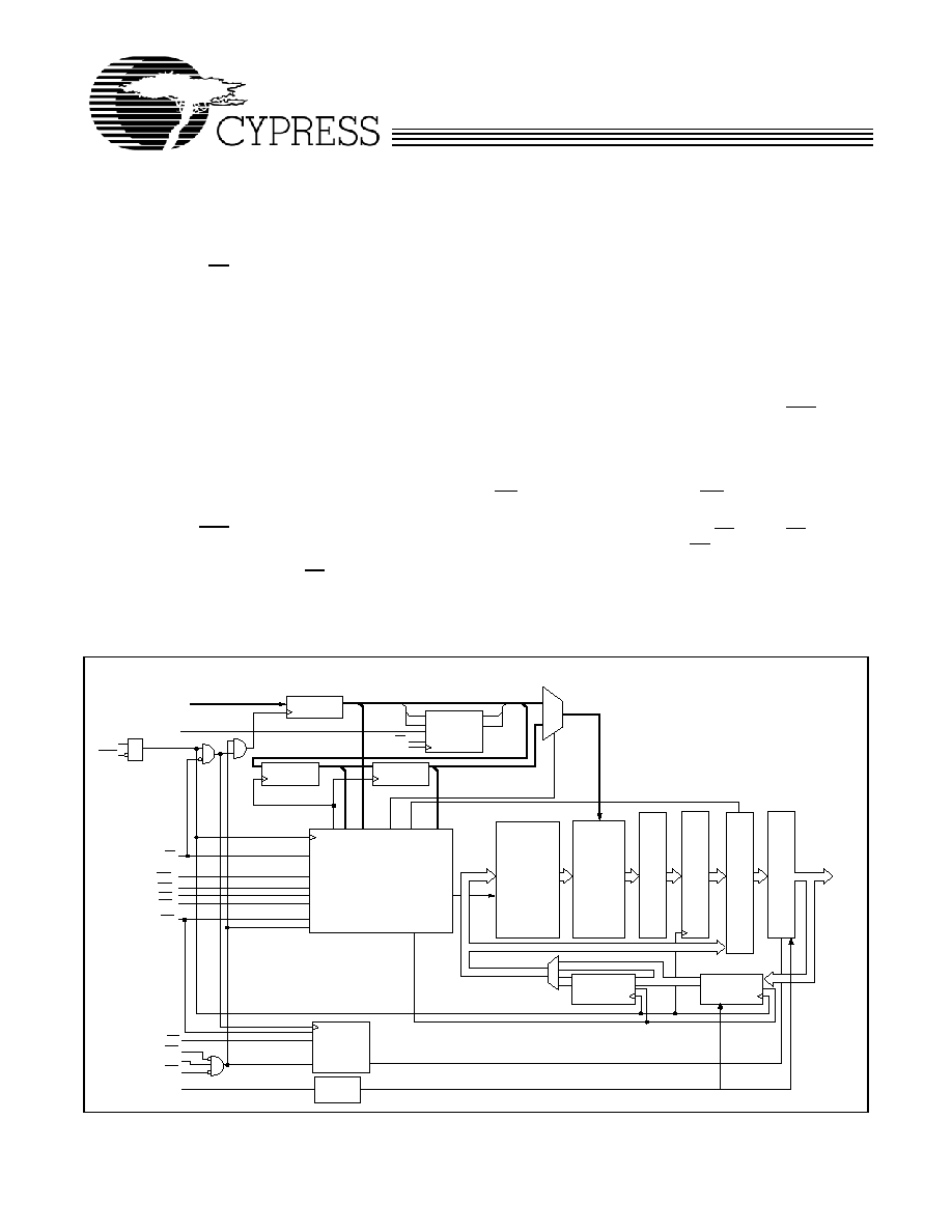
Functional Description
[1]
The CY7C1350F is a 3.3V, 128K x 36 synchronous-pipelined
Burst SRAM designed specifically to support unlimited true
back-to-back Read/Write operations without the insertion of
wait states. The CY7C1350F is equipped with the advanced
No Bus LatencyTM (NoBLTM) logic required to enable consec-
utive Read/Write operations with data being transferred on
every clock cycle. This feature dramatically improves the
throughput of the SRAM, especially in systems that require
frequent Write/Read transitions.
All synchronous inputs pass through input registers controlled
by the rising edge of the clock. All data outputs pass through
output registers controlled by the rising edge of the clock. The
clock input is qualified by the Clock Enable (CEN) signal,
which, when deasserted, suspends operation and extends the
previous clock cycle. Maximum access delay from the clock
rise is 2.8 ns (200-MHz device)
Write operations are controlled by the four Byte Write Select
(BW
[A:D]
) and a Write Enable (WE) input. All writes are
conducted with on-chip synchronous self-timed write circuitry.
Three synchronous Chip Enables (CE
1
, CE
2
, CE
3
) and an
asynchronous Output Enable (OE) provide for easy bank
selection and output three-state control. In order to avoid bus
contention, the output drivers are synchronously three-stated
during the data portion of a write sequence.
.
Note:
1. For best-practices recommendations, please refer to the Cypress application note System Design Guidelines on www.cypress.com.
A0, A1, A
C
MODE
BW
A
BW
B
WE
CE1
CE2
CE3
OE
READ LOGIC
DQs
DQP
A
DQP
B
DQP
C
DQP
D
D
A
T
A
S
T
E
E
R
I
N
G
O
U
T
P
U
T
B
U
F
F
E
R
S
MEMORY
ARRAY
E
E
INPUT
REGISTER 0
ADDRESS
REGISTER 0
WRITE ADDRESS
REGISTER 1
WRITE ADDRESS
REGISTER 2
WRITE REGISTRY
AND DATA COHERENCY
CONTROL LOGIC
BURST
LOGIC
A0'
A1'
D1
D0
Q1
Q0
A0
A1
C
ADV/LD
ADV/LD
E
INPUT
REGISTER 1
S
E
N
S
E
A
M
P
S
E
CLK
CEN
WRITE
DRIVERS
BW
C
BW
D
ZZ
SLEEP
CONTROL
O
U
T
P
U
T
R
E
G
I
S
T
E
R
S
Logic Block Diagram
CY7C1350F
Document #: 38-05305 Rev. *A
Page 3 of 16
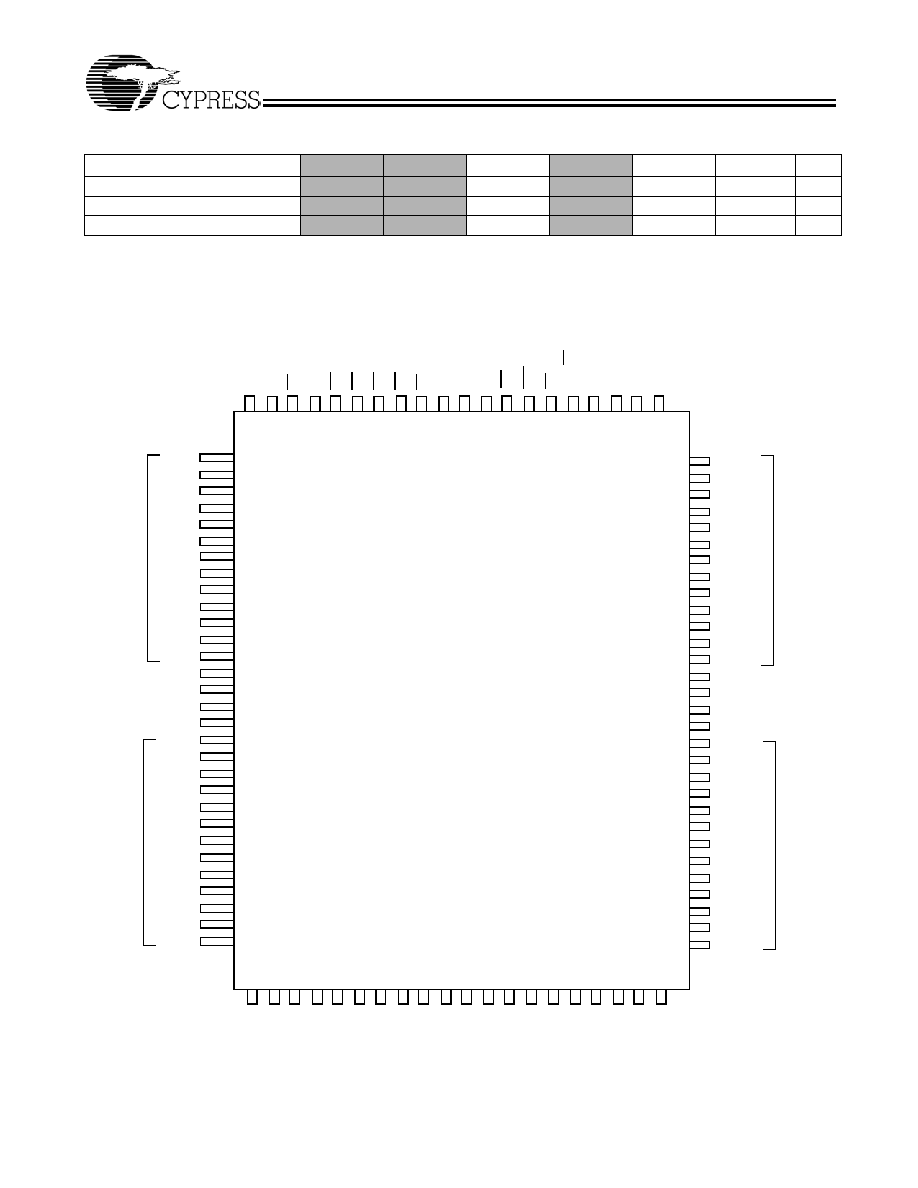
Pin Configuration
(continued)
2
3
4
5
6
7
1
A
B
C
D
E
F
G
H
J
K
L
M
N
P
R
T
U
DQ
A
V
DDQ
NC
NC
DQ
C
DQ
D
DQ
C
DQ
D
A
A
A
A
NC / 18M
V
DDQ
CE
2
A
V
DDQ
V
DDQ
V
DDQ
V
DDQ
NC
NC
A
DQ
C
DQ
C
DQ
D
DQ
D
NC
V
DD
A
NC / 72M
DQP
D
A
A
ADV/LD
A
CE
3
NC
V
DD
A
A
NC
V
SS
V
SS
NC
DQP
B
DQ
B
DQ
B
DQ
A
DQ
B
DQ
B
DQ
A
DQ
A
NC
NC
NC
V
DDQ
NC
V
SS
V
SS
V
SS
V
SS
V
SS
V
SS
V
SS
V
SS
MODE
CE
1
V
SS
OE
V
SS
V
DDQ
BW
C
NC / 9M
V
SS
WE
V
DDQ
V
DD
V
SS
V
DD
V
SS
CLK
NC
BW
A
CEN
V
SS
V
DDQ
V
SS
ZZ
NC
A
A
A1
A0
V
SS
V
DD
DQP
C
DQ
B
A
NC / 36M
DQ
C
DQ
B
DQ
C
DQ
C
DQ
C
DQ
B
DQ
B
DQ
A
DQ
A
DQ
A
DQ
A
DQP
A
DQ
D
DQ
D
DQ
D
DQ
D
BW
D
119-Ball Bump BGA
BW
B
NC
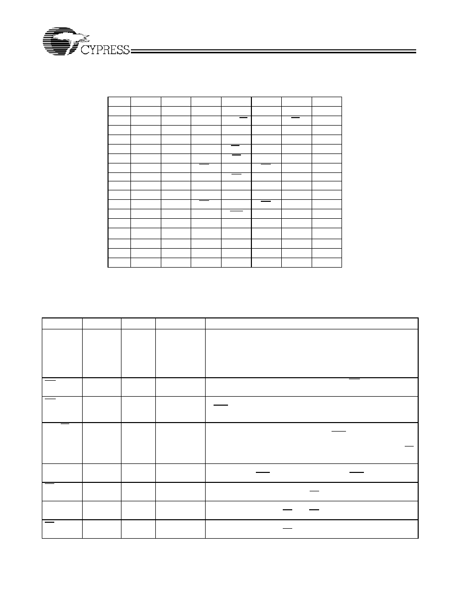
Pin Definitions
Name
119BGA
TQFP
I/O
Description
A0, A1, A
P4,N4,A2,
A3,A5,A6,
B3,B5,C2,
C3,C5,C6,
R2,R6,T3,
T4,T5
37,38,32,
33,34,35,
44,45,46,
47,48,49,
50,81,82,
99,10
Input-
Synchronous
Address Inputs used to select one of the 128K address locations.
Sampled at the rising edge of the CLK. A
[1:0]
are fed to the two-bit burst
counter.
BW
[A:D]
L5,G5,
G3,L3
93,94,
95,96
Input-
Synchronous
Byte Write Inputs, active LOW. Qualified with WE to conduct writes
to the SRAM. Sampled on the rising edge of CLK.
WE
H4
88
Input-
Synchronous
Write Enable Input, active LOW. Sampled on the rising edge of CLK
if CEN is active LOW. This signal must be asserted LOW to initiate a
write sequence.
ADV/LD
B4
85
Input-
Synchronous
Advance/Load Input. Used to advance the on-chip address counter
or load a new address. When HIGH (and CEN is asserted LOW) the
internal burst counter is advanced. When LOW, a new address can be
loaded into the device for an access. After being deselected, ADV/LD
should be driven LOW in order to load a new address.
CLK
K4
89
Input-Clock
Clock Input. Used to capture all synchronous inputs to the device. CLK
is qualified with CEN. CLK is only recognized if CEN is active LOW.
CE
1
E4
98
Input-
Synchronous
Chip Enable 1 Input, active LOW. Sampled on the rising edge of CLK.
Used in conjunction with CE
2
and CE
3
to select/deselect the device.
CE
2
B2
97
Input-
Synchronous
Chip Enable 2 Input, active HIGH. Sampled on the rising edge of CLK.
Used in conjunction with CE
1
and CE
3
to select/deselect the device.
CE
3
B6
92
Input-
Synchronous
Chip Enable 3 Input, active LOW. Sampled on the rising edge of CLK.
Used in conjunction with CE
1
and
CE
2
to select/deselect the device.
CY7C1350F
Document #: 38-05305 Rev. *A
Page 4 of 16
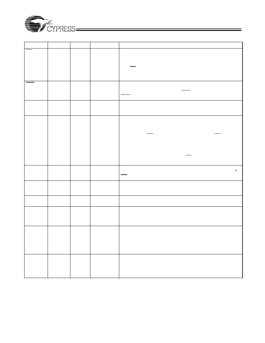
OE
F4
86
Input-
Asynchronous
Output Enable, asynchronous input, active LOW. Combined with
the synchronous logic block inside the device to control the direction of
the I/O pins. When LOW, the I/O pins are allowed to behave as outputs.
When deasserted HIGH, I/O pins are three-stated, and act as input data
pins. OE is masked during the data portion of a write sequence, during
the first clock when emerging from a deselected state, when the device
has been deselected.
CEN
M4
87
Input-
Synchronous
Clock Enable Input, active LOW. When asserted LOW the Clock sig-
nal is recognized by the SRAM. When deasserted HIGH the Clock
signal is masked. Since deasserting CEN does not deselect the device,
CEN can be used to extend the previous cycle when required.
ZZ
T7
64
Input-
Asynchronous
ZZ "sleep" Input. This active HIGH input places the device in a
non-time critical "sleep" condition with data integrity preserved. During
normal operation, this pin can be connected to Vss or left floating.
DQs
K6,K7,L6,
L7,M6,N6,
N7,P7,D7,
E6,E7,F6,
G6,G7,H6,
H7,D1,E1,
E2,F2,G1,
G2,H1,H2,
K1,K2,L1,
L2,M2,N1,
N2,P1
52,53,56,
57,58,59,
62,63,68,
69,72,73,
74,75,78,
79,2,3,6,
7,8,9,12,
13,18,19,
22,23,23,
24,25,28,
29
I/O-
Synchronous
Bidirectional Data I/O Lines. As inputs, they feed into an on-chip data
register that is triggered by the rising edge of CLK. As outputs, they
deliver the data contained in the memory location specified by the ad-
dress during the clock rise of the read cycle. The direction of the pins
is controlled by OE and the internal control logic. When OE is asserted
LOW, the pins can behave as outputs. When HIGH, DQ
s
and DQP
X
are
placed in a three-state condition. The outputs are automatically
three-stated during the data portion of a write sequence, during the first
clock when emerging from a deselected state, and when the device is
deselected, regardless of the state of OE.
DQP
[A:D]
P6,D6,
D2,P2
51,80,
1,30
I/O-
Synchronous
Bidirectional Data Parity I/O Lines. Functionally, these signals are
identical to DQ
s
. During write sequences, DQP
[A:D]
is controlled by
BW
[A:D]
correspondingly.
MODE
R3
31
Input
Strap pin
Mode Input. Selects the burst order of the device.
When tied to GND selects linear burst sequence. When tied to V
DD
or
left floating selects interleaved burst sequence.
V
DD
C4,J2,
J4,J6,R4
15,16,41,
65,66,91
Power Supply Power supply inputs to the core of the device.
V
DDQ
A1,A7,F1,
F7,J1,J7,
M1,M7,U1,
U7
4,11,14,
20,27,54,
61,70
I/O Power
Supply
Power supply for the I/O circuitry.
V
SS
D3,D5,E3,
E5,F3,F5
H3,H5,J3,
J5,K3,K5,
M3,M5,N3,
N5,P3,P5
5,10,17,2
1,26,40,5
5,60,67,
71,76,90
Ground
Ground for the device.
NC
A4,B1,B7,
C1,C7,D4,
G4,L4,R1,
R5,R7,T1,
T2,T6,U6
38,39,42,
43,83,84
No Connects. Not internally connected to the die.
9M, 18M, 36M, 72M, 144M and 288M are address expansion pins in
this device and will be used as address pins in their respective densi-
ties.
Pin Definitions
Name
119BGA
TQFP
I/O
Description

CY7C1350F
Document #: 38-05305 Rev. *A
Page 5 of 16
Introduction
Functional Overview
The CY7C1350F is a synchronous-pipelined Burst SRAM
designed specifically to eliminate wait states during
Write/Read transitions. All synchronous inputs pass through
input registers controlled by the rising edge of the clock. The
clock signal is qualified with the Clock Enable input signal
(CEN). If CEN is HIGH, the clock signal is not recognized and
all internal states are maintained. All synchronous operations
are qualified with CEN. All data outputs pass through output
registers controlled by the rising edge of the clock. Maximum
access delay from the clock rise (t
CO
) is 2.8 ns (200-MHz
device).
Accesses can be initiated by asserting all three Chip Enables
(CE
1
, CE
2
, CE
3
) active at the rising edge of the clock. If Clock
Enable (CEN) is active LOW and ADV/LD is asserted LOW,
the address presented to the device will be latched. The
access can either be a read or write operation, depending on
the status of the Write Enable (WE). BW
[A:D]
can be used to
conduct Byte Write operations.
Write operations are qualified by the Write Enable (WE). All
writes are simplified with on-chip synchronous self-timed write
circuitry.
Three synchronous Chip Enables (CE
1
, CE
2
, CE
3
) and an
asynchronous Output Enable (OE) simplify depth expansion.
All operations (Reads, Writes, and Deselects) are pipelined.
ADV/LD should be driven LOW once the device has been
deselected in order to load a new address for the next
operation.
Single Read Accesses
A read access is initiated when the following conditions are
satisfied at clock rise: (1) CEN is asserted LOW, (2) CE
1
, CE
2
,
and CE
3
are ALL asserted active, (3) the Write Enable input
signal WE is deasserted HIGH, and (4) ADV/LD is asserted
LOW. The address presented to the address inputs is latched
into the Address Register and presented to the memory core
and control logic. The control logic determines that a read
access is in progress and allows the requested data to
propagate to the input of the output register. At the rising edge
of the next clock the requested data is allowed to propagate
through the output register and onto the data bus, provided OE
is active LOW. After the first clock of the read access the output
buffers are controlled by OE and the internal control logic. OE
must be driven LOW in order for the device to drive out the
requested data. During the second clock, a subsequent
operation (Read/Write/Deselect) can be initiated. Deselecting
the device is also pipelined. Therefore, when the SRAM is
deselected at clock rise by one of the chip enable signals, its
output will three-state following the next clock rise.
Burst Read Accesses
The CY7C1350F has an on-chip burst counter that allows the
user the ability to supply a single address and conduct up to
four Reads without reasserting the address inputs. ADV/LD
must be driven LOW in order to load a new address into the
SRAM, as described in the Single Read Access section above.
The sequence of the burst counter is determined by the MODE
input signal. A LOW input on MODE selects a linear burst
mode, a HIGH selects an interleaved burst sequence. Both
burst counters use A0 and A1 in the burst sequence, and will
wrap around when incremented sufficiently. A HIGH input on
ADV/LD will increment the internal burst counter regardless of
the state of chip enables inputs or WE. WE is latched at the
beginning of a burst cycle. Therefore, the type of access (Read
or Write) is maintained throughout the burst sequence.
Single Write Accesses
Write accesses are initiated when the following conditions are
satisfied at clock rise: (1) CEN is asserted LOW, (2) CE
1
, CE
2
,
and CE
3
are ALL asserted active, and (3) the Write signal WE
is asserted LOW. The address presented to the address inputs
is loaded into the Address Register. The write signals are
latched into the Control Logic block.
On the subsequent clock rise the data lines are automatically
three-stated regardless of the state of the OE input signal. This
allows the external logic to present the data on DQs
and
DQP
[A:D]
. In addition, the address for the subsequent access
(Read/Write/Deselect) is latched into the Address Register
(provided the appropriate control signals are asserted).
On the next clock rise the data presented to DQs
and DQP
[A:D]
(or a subset for Byte Write operations, see Write Cycle
Description table for details) inputs is latched into the device
and the write is complete.
The data written during the Write operation is controlled by
BW
[A:D]
signals. The CY7C1350F provides byte write
capability that is described in the Write Cycle Description table.
Asserting the Write Enable input (WE) with the selected Byte
Write Select (BW
[A:D]
) input will selectively write to only the
desired bytes. Bytes not selected during a Byte Write
operation will remain unaltered. A synchronous self-timed
write mechanism has been provided to simplify the write
operations. Byte write capability has been included in order to
greatly simplify Read/Modify/Write sequences, which can be
reduced to simple byte write operations.
Because the CY7C1350F is a common I/O device, data should
not be driven into the device while the outputs are active. The
Output Enable (OE) can be deasserted HIGH before
presenting data to the DQs
and DQP
[A:D]
inputs. Doing so will
tri-state the output drivers. As a safety precaution, DQs
and
DQP
[A:D]
are automatically three-stated during the data
portion of a write cycle, regardless of the state of OE.
Burst Write Accesses
The CY7C1350F has an on-chip burst counter that allows the
user the ability to supply a single address and conduct up to
four Write operations without reasserting the address inputs.
ADV/LD must be driven LOW in order to load the initial
address, as described in the Single Write Access section
above. When ADV/LD is driven HIGH on the subsequent clock
rise, the chip enables (CE
1
, CE
2
, and CE
3
) and WE inputs are
ignored and the burst counter is incremented. The correct
BW
[A:D]
inputs must be driven in each cycle of the burst write
in order to write the correct bytes of data.
Sleep Mode
The ZZ input pin is an asynchronous input. Asserting ZZ
places the SRAM in a power conservation "sleep" mode. Two
clock cycles are required to enter into or exit from this "sleep"
mode. While in this mode, data integrity is guaranteed.
Accesses pending when entering the "sleep" mode are not
considered valid nor is the completion of the operation
guaranteed. The device must be deselected prior to entering
the "sleep" mode. CE
1
, CE
2
, and CE
3
, must remain inactive
for the duration of t
ZZREC
after the ZZ input returns LOW.