
4K x 8 Dual-Port Static RAM and 4K x 8 Dual-Port
SRAM with Semaphores
CY7C135
CY7C1342
Cypress Semiconductor Corporation
·
3901 North First Street
·
San Jose
·
CA 95134
·
408-943-2600
Document #: 38-06038 Rev. *B
Revised June 22, 2004
Features
· True Dual-Ported memory cells which allow simulta-
neous reads of the same memory location
· 4K x 8 organization
· 0.65-micron CMOS for optimum speed/power
· High-speed access: 15 ns
· Low operating power: I
CC
= 160 mA (max.)
· Fully asynchronous operation
· Automatic power-down
· Semaphores included on the 7C1342 to permit software
handshaking between ports
· Available in 52-pin PLCC
Functional Description
The CY7C135 and CY7C1342 are high-speed CMOS 4K x 8
dual-port static RAMs. The CY7C1342 includes semaphores
that provide a means to allocate portions of the dual-port RAM
or any shared resource. Two ports are provided permitting in-
dependent, asynchronous access for reads and writes to any
location in memory. Application areas include interproces-
sor/multiprocessor designs, communications status buffering,
and dual-port video/graphics memory.
Each port has independent control pins: chip enable (CE),
read or write enable (R/W), and output enable (OE). The
CY7C135 is suited for those systems that do not require
on-chip arbitration or are intolerant of wait states. Therefore,
the user must be aware that simultaneous access to a location
is possible. Semaphores are offered on the CY7C1342 to as-
sist in arbitrating between ports. The semaphore logic is com-
prised of eight shared latches. Only one side can control the
latch (semaphore) at any time. Control of a semaphore indi-
cates that a shared resource is in use. An automatic pow-
er-down feature is controlled independently on each port by a
chip enable (CE) pin or SEM pin (CY7C1342 only).
The CY7C135 and CY7C1342 are available in 52-pin PLCC.
13421
R/W
L
CE
L
OE
L
A
11L
A
0L
A
0R
A
11R
R/W
R
CE
R
OE
R
CE
R
OE
R
CE
L
OE
L
R/W
L
R/W
R
I/O
7L
I/O
0L
I/O
7R
I/O
0R
SEMAPHORE
ARBITRATION
(7C1342 only)
CONTROL
I/O
CONTROL
I/O
MEMORY
ARRAY
ADDRESS
DECODER
ADDRESS
DECODER
(7C1342 only)
SEM
L
SEM
R
Logic Block Diagram
(7C1342 only)
CY7C135
CY7C1342
Document #: 38-06038 Rev. *B
Page 2 of 12
Selection Guide
7C13515
7C134215
7C13520
7C134220
7C13525
7C134225
7C13535
7C134235
7C13555
7C134255
Maximum Access Time (ns)
15
20
25
35
55
Maximum Operating
Current (mA)
Commercial
220
190
180
160
160
Maximum Standby
Current for I
SB1
(mA)
Commercial
60
50
40
30
30
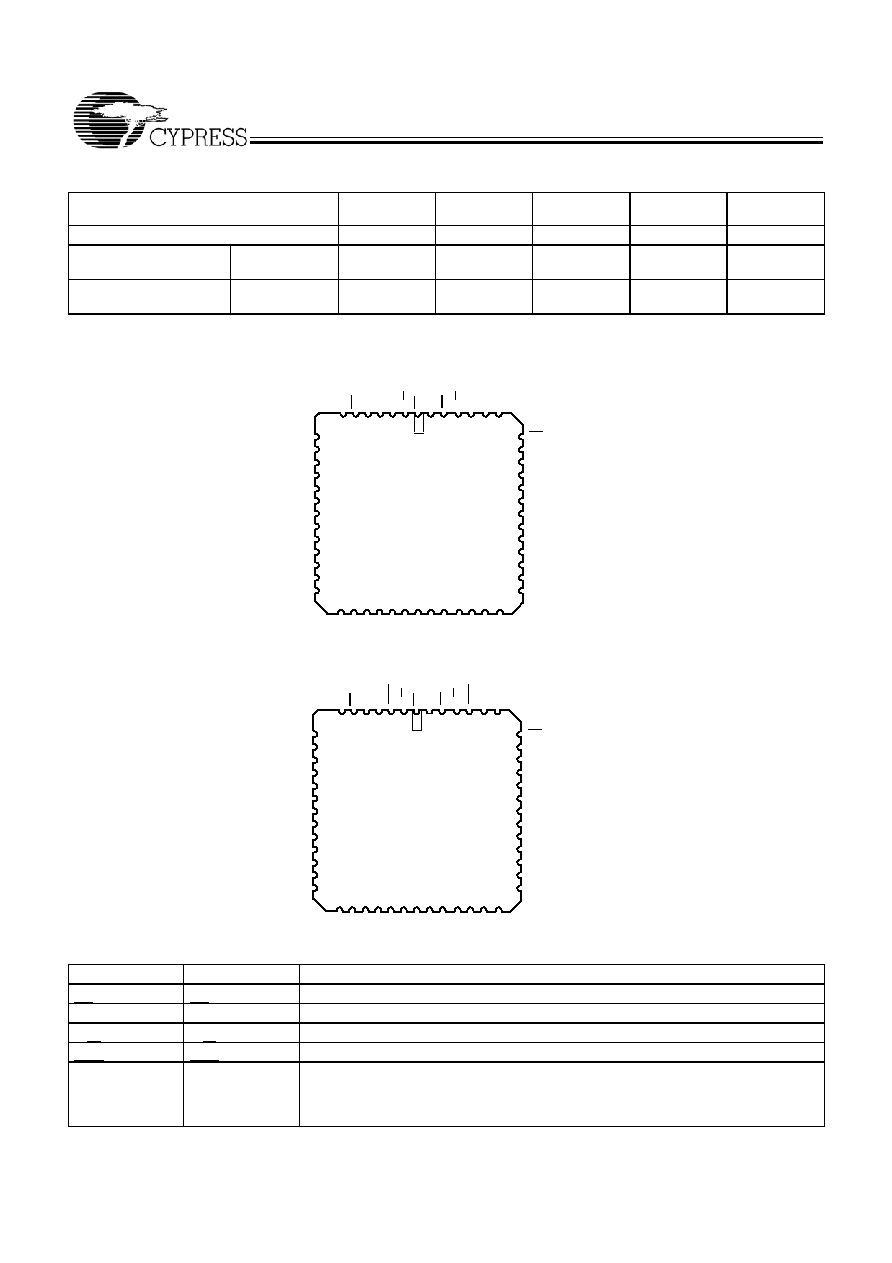
Pin Configurations
A 11
R
1
V
CC
7C1342
Top View
PLCC
8
9
10
11
12
13
14
15
16
17
18
19
20
46
45
44
43
42
41
40
39
38
37
36
35
34
21 22 23 24 25 26 27 28 29 30 31 32 33
7 6 5 4 3 2
52 51 50 49 48 47
I/O
I/O
I/O
I/O
I/O
I/O
I/O
I/O
I/O
I/O
I/O
4L
5L
6L
7L
0R
1R
2R
3R
4R
5R
6R
NC
GN
D
OE
SE
M
A
R/W
CE
R/W
SE
M
0L
L
L
L
L
CE
R
R
R
A 10L
A 10
R
OE
R
A
0R
A
1R
A
2R
A
3R
A
4R
A
5R
A
6R
A
7R
A
8R
A
9R
NC
I/O
7R
A
1L
A
2L
A
3L
A
4L
A
5L
A
6L
A
7L
A
8L
A
9L
I/O
0L
I/O
1L
I/O
2L
I/O
3L
1
V
CC
7C135
Top View
PLCC
8
9
10
11
12
13
14
15
16
17
18
19
20
46
45
44
43
42
41
40
39
38
37
36
35
34
21 22 23 24 25 26 27 28 29 30 31 32 33
7 6 5 4 3 2
52 51 50 49 48 47
I/
O
I/
O
I/
O
I/
O
I/
O
I/
O
I/
O
I/
O
I/
O
I/
O
I/
O
4L
5L
6L
7L
0R
1R
2R
3R
4R
5R
6R
NC
GND
OE
N/
C
A
R/
W
CE
R/
W
0L
L
L
L
CE
R
R
A 10L
A 10
R
OE
R
A
0R
A
1R
A
2R
A
3R
A
4R
A
5R
A
6R
A
7R
A
8R
A
9R
NC
I/O
7R
A
1L
A
2L
A
3L
A
4L
A
5L
A
6L
A
7L
A
8L
A
9L
I/O
0L
I/O
1L
I/O
2L
I/O
3L
N/
C
A 11
R
A 11L
A 11L
13423
13424
Pin Definitions
Left Port
Right Port
Description
A
0L11L
A
0R11R
Address Lines
CE
L
CE
R
Chip Enable
OE
L
OE
R
Output Enable
R/W
L
R/W
R
Read/Write Enable
SEM
L
(CY7C1342 only)
SEM
R
(CY7C1342 only)
Semaphore Enable. When asserted LOW, allows access to eight semaphores. The
three least significant bits of the address lines will determine which semaphore to write
or read. The I/O
0
pin is used when writing to a semaphore. Semaphores are requested
by writing a 0 into the respective location.

CY7C135
CY7C1342
Document #: 38-06038 Rev. *B
Page 3 of 12
Maximum Ratings
[1]
Storage Temperature ..................................65
°
C to +150
°
C
Ambient Temperature with
Power Applied..............................................55
°
C to +125
°
C
Supply Voltage to Ground Potential
(Pin 48 to Pin 24) ............................................ 0.5V to +7.0V
DC Voltage Applied to Outputs
in High Z State ................................................ 0.5V to +7.0V
DC Input Voltage
[2]
......................................... 3.0V to +7.0V
Static Discharge Voltage........................................... > 2001V
(per MIL-STD-883, Method 3015)
Latch-Up Current.................................................... > 200 mA
Operating Range
Range
Ambient
Temperature
V
CC
Commercial
0
°
C to +70
°
C
5V ± 10%
Industrial
40
°
C to +85
°
C
5V ± 10%
Electrical Characteristics
Over the Operating Range
[4]
7C13515
7C13421
5
7C13520
7C13422
0
7C13525
7C134225
Parameter
Description
Test Conditions
Min.
Max
.
Min
.
Max
.
Min.
Max
.
Uni
t
V
OH
Output HIGH Voltage
V
CC
= Min., I
OH
= 4.0 mA
2.4
2.4
2.4
V
V
OL
Output LOW Voltage
V
CC
= Min., I
OL
= 4.0 mA
0.4
0.4
0.4
V
V
IH
Input HIGH Voltage
2.2
2.2
2.2
V
V
IL
Input LOW Voltage
0.8
0.8
0.8
V
I
IX
Input Load Current
GND
V
I
V
CC
10
+10
10
+10
10
+10
µ
A
I
OZ
Output Leakage Current
Outputs Disabled,
GND
V
O
V
CC
10
+10
10
+10
10
+10
µ
A
I
CC
Operating Current
V
CC
= Max.,
I
OUT
= 0 mA
Com'l
220
190
180
mA
Ind.
190
I
SB1
Standby Current
(Both Ports TTL Levels)
CE
L
and CE
R
V
IH
,
f = f
MAX
[5]
Com'l
60
50
40
mA
Ind.
50
I
SB2
Standby Current
(One Port TTL Level)
CE
L
and CE
R
V
IH
,
f = f
MAX
[5]
Com'l
130
120
110
mA
Ind.
120
I
SB3
Standby Current
(Both Ports CMOS Levels)
Both Ports CE and CE
R
V
CC
0.2V,
V
IN
V
CC
0.2V
or V
IN
0.2V, f = 0
[5]
Com'l
15
15
15
mA
Ind.
30
I
SB4
Standby Current
(One Port CMOS Level)
One Port CE
L
or
CE
R
V
CC
0.2V,
V
IN
V
CC
0.2V or V
IN
0.2V,
Active Port Outputs, f =
f
MAX
[5]
Com'l
125
115
100
mA
Ind.
115
Notes:
1.
The Voltage on any input or I/O pin cannot exceed the power pin during power-up.
2.
Pulse width < 20 ns.
3.
T
A
is the "instant on" case temperature.
4.
See the last page of this specification for Group A subgroup testing information.
5.
f
MAX
= 1/t
RC
= All inputs cycling at f = 1/t
RC
(except output enable). f = 0 means no address or control lines change. This applies only to inputs at CMOS level standby I
SB3
.

CY7C135
CY7C1342
Document #: 38-06038 Rev. *B
Page 4 of 12
Electrical Characteristics
Over the Operating Range
[4]
(continued)
7C13535
7C134235
7C13555
7C134255
Parameter
Description
Test Conditions
Min. Max. Min. Max. Unit
V
OH
Output HIGH Voltage
V
CC
= Min., I
OH
= 4.0 mA
2.4
2.4
V
V
OL
Output LOW Voltage
V
CC
= Min., I
OL
= 4.0 mA
0.4
0.4
V
V
IH
2.2
2.2
V
V
IL
Input LOW Voltage
0.8
0.8
V
I
IX
Input Load Current
GND
V
I
V
CC
10
+10
10
+10
µ
A
I
OZ
Output Leakage Current
Outputs Disabled, GND
V
O
V
CC
10
+10
10
+10
µ
A
I
CC
Operating Current
V
CC
= Max., I
OUT
= 0 mA
Com'l
160
160
mA
V
CC
= Max., I
OUT
= 0 mA
Ind.
180
180
I
SB1
Standby Current
(Both Ports TTL Levels)
CE
L
and CE
R
V
IH
, f = f
MAX
[5]
Com'l
30
30
mA
Ind.
40
40
I
SB2
Standby Current
(One Port TTL Level)
CE
L
and CE
R
V
IH
, f = f
MAX
[5]
Com'l
100
100
mA
Ind.
110
110
I
SB3
Standby Current
(Both Ports CMOS Levels)
Both Ports CE and CE
R
V
CC
0.2V,
V
IN
V
CC
0.2V
or V
IN
0.2V, f = 0
[5]
Com'l
15
15
mA
Ind.
30
30
I
SB4
Standby Current
(One Port CMOS Level)
One Port CE
L
or CE
R
V
CC
0.2V,
V
IN
V
CC
0.2V or V
IN
0.2V,
Active Port Outputs, f = f
MAX
[5]
Com'l
90
90
mA
Ind.
100
100
Capacitance
[6]
Parameter
Description
Test Conditions
Max.
Unit
C
IN
Input Capacitance
T
A
= 25
°
C, f = 1 MHz,
V
CC
= 5.0V
10
pF
C
OUT
Output Capacitance
10
pF
AC Test Loads and Waveforms
Note:
6.
Tested initially and after any design or process changes that may affect these parameters.
3.0V
GND
90%
90%
10%
3 ns
3 ns
10%
ALL INPUT PULSES
(a) Normal Load (Load 1)
R1= 893
5V
OUTPUT
R1= 347
C= 30pF
R
TH
= 250
V
TH
= 1.4V
OUTPUT
C= 30pF
(b) Thévenin Equivalent (Load 1)
(c) Three-State Delay (Load 3)
R
TH
= 250
V
X
OUTPUT
C = 5 pF
13425
13426
13427
13428

CY7C135
CY7C1342
Document #: 38-06038 Rev. *B
Page 5 of 12
Switching Characteristics
Over the Operating Range
[7, 8]
7C13515
7C134215
7C13520
7C134220
7C13525
7C134225
7C13535
7C134235
7C13555
7C134255
Parameter
Description
Min. Max. Min. Max. Min. Max. Min. Max. Min. Max.
Unit
READ CYCLE
t
RC
Read Cycle Time
15
20
25
35
55
ns
t
AA
Address to Data Valid
15
20
25
35
55
ns
t
OHA
Output Hold From
Address Change
3
3
3
3
3
ns
t
ACE
CE LOW to Data Valid
15
20
25
35
55
ns
t
DOE
OE LOW to Data Valid
10
13
15
20
25
ns
t
LZOE
[9,10,11]
OE Low to Low Z
3
3
3
3
3
ns
t
HZOE
[9,10,11]
OE HIGH to High Z
10
13
15
20
25
ns
t
LZCE
[9,10,11]
CE LOW to Low Z
3
3
3
3
3
ns
t
HZCE
[9,10,11]
CE HIGH to High Z
10
13
15
20
25
ns
t
PU
[11]
CE LOW to Power Up
0
0
0
0
0
ns
t
PD
[11]
CE HIGH to Power Down
15
20
25
35
55
ns
WRITE CYCLE
t
WC
Write Cycle Time
15
20
25
35
55
ns
t
SCE
CE LOW to Write End
12
15
20
30
50
ns
t
AW
Address Set-Up to Write End
12
15
20
30
50
ns
t
HA
Address Hold from Write End
2
2
2
2
2
ns
t
SA
Address Set-Up to Write Start
0
0
0
0
0
ns
t
PWE
Write Pulse Width
12
15
20
25
50
ns
t
SD
Data Set-Up to Write End
10
13
15
15
25
ns
t
HD
Data Hold from Write End
0
0
0
0
0
ns
t
HZWE
[10,11]
R/W LOW to High Z
10
13
15
20
25
ns
t
LZWE
[10,11]
R/W HIGH to Low Z
3
3
3
3
3
ns
t
WDD
[12]
Write Pulse to Data Delay
30
40
50
60
70
ns
t
DDD
[12]
Write Data Valid to Read
Data Valid
25
30
30
35
40
ns
SEMAPHORE TIMING
[13]
t
SOP
SEM Flag Update Pulse
(OE or SEM)
10
10
10
15
15
ns
t
SWRD
SEM Flag Write to Read Time
5
5
5
5
5
ns
t
SPS
SEM Flag Contention Window
5
5
5
5
5
ns
Notes:
7.
See the last page of this specification for Group A subgroup testing information.
8.
Test conditions assume signal transition time of 3 ns or less, timing reference levels of 1.5V, input pulse levels of 0 to 3.0V, and output loading of the specified
I
OL
/I
OH
and 30-pF load capacitance.
9.
At any given temperature and voltage condition for any given device, t
HZCE
is less than t
LZCE
and t
HZOE
is less than t
LZOE
.
10. Test conditions used are Load 3.
11. This parameter is guaranteed but not tested.
12. For information on port-to-port delay through RAM cells from writing port to reading port, refer to Read Timing with Port-to-Port Delay waveform.
13. Semaphore timing applies only to CY7C1342.