64K x 32 Synchronous-Pipelined Cache RAM
CY7C1329
Cypress Semiconductor Corporation
·
3901 North First Street
·
San Jose
·
CA 95134
·
408-943-2600
August 6, 1999
Features
· Supports 133-MHz bus for Pentium® and PowerPCTM
operations with zero wait states
· Fully registered inputs and outputs for pipelined
operation
· 64K x 32 common I/O architecture
· Single 3.3V power supply
· Fast clock-to-output times
-- 4.2 ns (for 133-MHz device)
-- 5.5 ns (for 100-MHz device)
-- 7.0 ns (for 75-MHz device
· User-selectable burst counter supporting Intel®
Pentium interleaved or linear burst sequences
· Separate processor and controller address strobes
· Synchronous self-timed writes
· Asynchronous output enable
· JEDEC-standard 100 TQFP pinout
· "ZZ" Sleep Mode option and Stop Clock option
Functional Description
The CY7C1329 is a 3.3V, 64K by 32 synchronous-pipelined
cache SRAM designed to support zero wait state secondary
cache with minimal glue logic.
All synchronous inputs pass through input registers controlled
by the rising edge of the clock. All data outputs pass through
output registers controlled by the rising edge of the clock. Max-
imum access delay from the clock rise is 4.2 ns (133-MHz
device).
The CY7C1329 supports either the interleaved burst se-
quence used by the Intel Pentium processor or a linear burst
sequence used by processors such as the PowerPC. The burst
sequence is selected through the MODE pin. Accesses can
be initiated by asserting either the Processor Address Strobe
(ADSP) or the Controller Address Strobe (ADSC) at clock rise.
Address advancement through the burst sequence is con-
trolled by the ADV input. A 2-bit on-chip wraparound burst
counter captures the first address in a burst sequence and
automatically increments the address for the rest of the burst
access.
Byte write operations are qualified with the four Byte Write
Select (BW
[3:0]
) inputs. A Global Write Enable (GW) overrides
all byte write inputs and writes data to all four bytes. All writes
are conducted with on-chip synchronous self-timed write cir-
cuitry.
Three synchronous Chip Selects (CE
1
, CE
2
, CE
3
) and an
asynchronous Output Enable (OE) provide for easy bank se-
lection and output three-state control. In order to provide prop-
er data during depth expansion, OE is masked during the first
clock of a read cycle when emerging from a deselected state.
Intel and Pentium are registered trademarks of Intel Corporation.
PowerPC is a trademark of IBM Corporation.
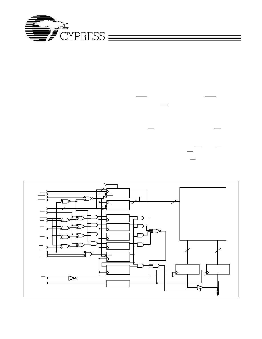
CLK
ADV
ADSC
A
[15:0]
GW
BWE
BW
3
BW
2
BW
1
BW
0
CE
1
CE
3
CE
2
OE
ZZ
BURST
COUNTER
DQ[31:24]
BYTEWRITE
REGISTERS
ADDRESS
REGISTER
D
Q
OUTPUT
REGISTERS
INPUT
REGISTERS
64KX32
MEMORY
ARRAY
CLK
CLK
Q
0
Q
1
Q
D
CE
CE
CLR
SLEEP
CONTROL
DQ[23:16]
BYTEWRITE
REGISTERS
D
Q
D
Q
DQ[15:8]
BYTEWRITE
REGISTERS
DQ[7:0]
BYTEWRITE
REGISTERS
D
Q
ENABLE
REGISTER
D
Q
CE
CLK
ENABLE DELAY
REGISTER
D
Q
CLK
32
32
16
14
14
16
(A
[1:0]
)
2
MODE
ADSP
Logic Block Diagram
DQ
[31:0]

CY7C1329
2
Pin Configuration
A
5
A
4
A
3
A
2
A
1
A
0
NC
NC
V
SS
V
DD
NC
NC
A
10
A
11
A
12
A
13
A
14
A
15
NC
NC
DQ
15
DQ
14
V
DDQ
V
SSQ
DQ
13
DQ
12
DQ
11
DQ
10
V
SSQ
V
DDQ
DQ
9
DQ
8
V
SS
NC
V
DD
ZZ
DQ
7
DQ
6
V
DDQ
V
SSQ
DQ
5
DQ
4
DQ
3
DQ
2
V
SSQ
V
DDQ
DQ
1
DQ
0
NC
NC
DQ
16
DQ
17
V
DDQ
V
SSQ
DQ
18
DQ
19
DQ
20
DQ
21
V
SSQ
V
DDQ
DQ
22
DQ
23
NC
V
DD
NC
V
SS
DQ
24
DQ
25
V
DDQ
V
SSQ
DQ
26
DQ
27
DQ
28
DQ
29
V
SSQ
V
DDQ
DQ
30
DQ
31
NC
A6
A7
CE
1
CE
2
BW
3
BW
2
BW
1
BW
0
CE
3
V
DD
V
SS
CL
K
GW
BW
E
OE
AD
S
C
AD
S
P
AD
V
A
8
A
9
1
2
3
4
5
6
7
8
9
10
11
12
13
14
15
16
17
18
19
20
21
22
23
24
25
26
27
28
29
30
31
32
33
34
35
36
37
38
39
40
41
42
43
44
45
46
47
48
49
50
80
79
78
77
76
75
74
73
72
71
70
69
68
67
66
65
64
63
62
61
60
59
58
57
56
55
54
53
52
51
10
0
99
98
97
96
95
94
93
92
91
90
89
88
87
86
85
84
83
82
81
MO
D
E
BYTE0
BYTE1
BYTE3
BYTE2
100-Pin TQFP
CY7C1329
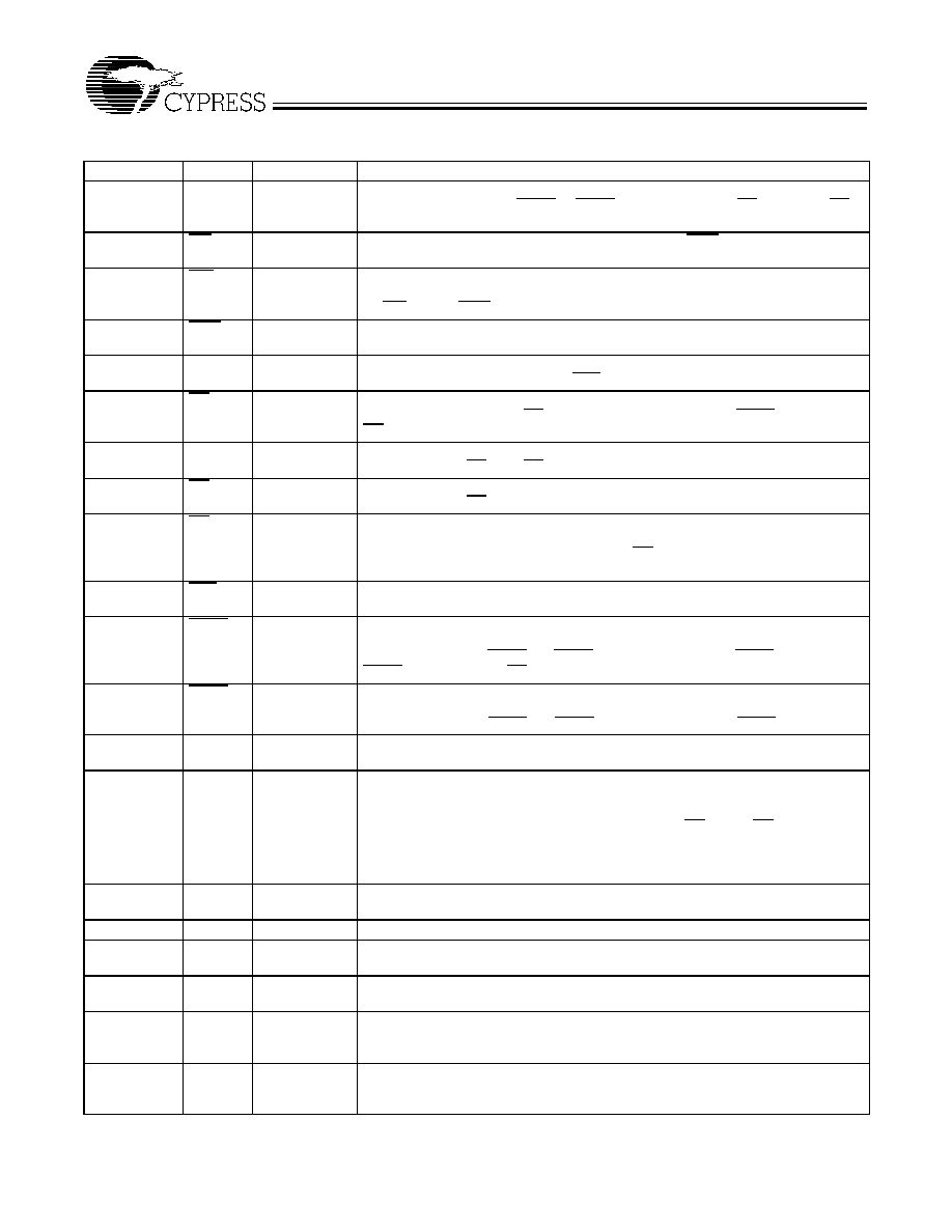
Selection Guide
7C1329-133
7C1329-100
7C1329-75
Maximum Access Time (ns)
4.2
5.5
7.0
Maximum Operating Current (mA)
Commercial
325
310
260
Maximum CMOS Standby Current (mA)
Commercial
5
5
5
CY7C1329
3
Pin Definitions
Pin Number
Name
I/O
Description
4944, 81,82,
99, 100,
3237
A
[15:0]
Input-
Synchronous
Address Inputs used to select one of the 64K address locations. Sampled at the
rising edge of the CLK if ADSP or ADSC is active LOW, and CE
1
,
CE
2
, and
CE
3
are sampled active. A
[1:0]
feed the 2-bit counter.
9693
BW
[3:0]
Input-
Synchronous
Byte Write Select Inputs, active LOW. Qualified with BWE to conduct byte writes
to the SRAM. Sampled on the rising edge of CLK.
88
GW
Input-
Synchronous
Global Write Enable Input, active LOW. When asserted LOW on the rising edge of
CLK, a global write is conducted (ALL bytes are written, regardless of the values
on BW
[3:0]
and BWE).
87
BWE
Input-
Synchronous
Byte Write Enable Input, active LOW. Sampled on the rising edge of CLK. This
signal must be asserted LOW to conduct a byte write.
89
CLK
Input-Clock
Clock input. Used to capture all synchronous inputs to the device. Also used to
increment the burst counter when ADV is asserted LOW, during a burst operation.
98
CE
1
Input-
Synchronous
Chip Enable 1 Input, active LOW. Sampled on the rising edge of CLK. Used in
conjunction with CE
2
and CE
3
to select/deselect the device. ADSP is ignored if
CE
1
is HIGH.
97
CE
2
Input-
Synchronous
Chip Enable 2 Input, active HIGH. Sampled on the rising edge of CLK. Used in
conjunction with CE
1
and CE
3
to select/deselect the device.
92
CE
3
Input-
Synchronous
Chip Enable 3 Input, active LOW. Sampled on the rising edge of CLK. Used in
conjunction with CE
1
and
CE
2
to select/deselect the device.
86
OE
Input-
Asynchronous
Output Enable, asynchronous input, active LOW. Controls the direction of the I/O
pins. When LOW, the I/O pins behave as outputs. When deasserted HIGH, I/O pins
are three-stated, and act as input data pins. OE is masked during the first clock of
a read cycle when emerging from a deselected state.
83
ADV
Input-
Synchronous
Advance Input signal, sampled on the rising edge of CLK. When asserted, it auto-
matically increments the address in a burst cycle.
84
ADSP
Input-
Synchronous
Address Strobe from Processor, sampled on the rising edge of CLK. When assert-
ed LOW, A
[15:0]
is captured in the address registers. A
[1:0]
are also loaded into the
burst counter. When ADSP and ADSC are both asserted, only ADSP is recognized.
ASDP is ignored when CE
1
is deasserted HIGH.
85
ADSC
Input-
Synchronous
Address Strobe from Controller, sampled on the rising edge of CLK. When assert-
ed LOW, A
[15:0]
is captured in the address registers. A
[1:0]
are also loaded into the
burst counter. When ADSP and ADSC are both asserted, only ADSP is recognized.
64
ZZ
Input-
Asynchronous
ZZ "sleep" Input. This active HIGH input places the device in a non-time critical
"sleep" condition with data integrity preserved.
29, 28,
2522, 19,
18,13,12,
96, 3, 2, 79,
78, 7572,
69, 68, 63, 62
5956, 53, 52
DQ
[31:0]
I/O-
Synchronous
Bidirectional Data I/O lines. As inputs, they feed into an on-chip data register that
is triggered by the rising edge of CLK. As outputs, they deliver the data contained
in the memory location specified by A
[15:0]
during the previous clock rise of the
read cycle. The direction of the pins is controlled by OE. When OE is asserted
LOW, the pins behave as outputs. When HIGH, DQ
[31:0]
are placed in a three-state
condition.
15, 41, 65, 91
V
DD
Power Supply
Power supply inputs to the core of the device. Should be connected to 3.3V power
supply.
17, 40, 67, 90
V
SS
Ground
Ground for the core of the device. Should be connected to ground of the system.
4, 11, 20, 27,
54, 61, 70, 77
V
DDQ
I/O Power
Supply
Power supply for the I/O circuitry. Should be connected to a 3.3V power supply.
5, 10, 21, 26,
55, 60, 71, 76
V
SSQ
I/O Ground
Ground for the I/O circuitry. Should be connected to ground of the system.
31
MODE
Input-
Static
Selects burst order. When tied to GND selects linear burst sequence. When tied
to V
DDQ
or left floating selects interleaved burst sequence. This is a strap pin and
should remain static during device operation.
1, 14, 16, 30,
38, 39, 42, 43,
50, 51, 66, 80
NC
-
No Connects.

CY7C1329
4
Introduction
Functional Overview
All synchronous inputs pass through input registers controlled
by the rising edge of the clock. All data outputs pass through
output registers controlled by the rising edge of the clock. Max-
imum access delay from the clock rise (t
CO
) is 4.2 ns (133-MHz
device).
The CY7C1329 supports secondary cache in systems utilizing
either a linear or interleaved burst sequence. The interleaved
burst order supports Pentium and i486 processors. The linear
burst sequence is suited for processors that utilize a linear
burst sequence. The burst order is user selectable, and is de-
termined by sampling the MODE input. Accesses can be initi-
ated with either the Processor Address Strobe (ADSP) or the
Controller Address Strobe (ADSC). Address advancement
through the burst sequence is controlled by the ADV input. A
two-bit on-chip wraparound burst counter captures the first ad-
dress in a burst sequence and automatically increments the
address for the rest of the burst access.
Byte write operations are qualified with the Byte Write Enable
(BWE) and Byte Write Select (BW
[3:0]
) inputs. A Global Write
Enable (GW) overrides all byte write inputs and writes data to
all four bytes. All writes are simplified with on-chip synchro-
nous self-timed write circuitry.
Three synchronous Chip Selects (CE
1
, CE
2
, CE
3
) and an
asynchronous Output Enable (OE) provide for easy bank se-
lection and output three-state control. ADSP is ignored if CE
1
is HIGH.
Single Read Accesses
This access is initiated when the following conditions are sat-
isfied at clock rise: (1) ADSP or ADSC is asserted LOW, (2)
CE
1
, CE
2
, CE
3
are all asserted active, and (3) the write signals
(GW, BWE) are all deasserted HIGH. ADSP is ignored if CE
1
is HIGH. The address presented to the address inputs (A
[15:0]
)
is stored into the address advancement logic and the Address
Register while being presented to the memory core. The cor-
responding data is allowed to propagate to the input of the
Output Registers. At the rising edge of the next clock the data
is allowed to propagate through the output register and onto
the data bus within 4.2 ns (133-MHz device) if OE is active
LOW. The only exception occurs when the SRAM is emerging
from a deselected state to a selected state, its outputs are
always three-stated during the first cycle of the access. After
the first cycle of the access, the outputs are controlled by the
OE signal. Consecutive single read cycles are supported.
Once the SRAM is deselected at clock rise by the chip select
and either ADSP or ADSC signals, its output will three-state
immediately.
Single Write Accesses Initiated by ADSP
This access is initiated when both of the following conditions
are satisfied at clock rise: (1) ADSP is asserted LOW, and (2)
CE
1
, CE
2
, CE
3
are all asserted active. The address presented
to A
[15:0]
is loaded into the address register and the address
advancement logic while being delivered to the RAM core. The
write signals (GW, BWE, and BW
0
BW
3
) and ADV inputs are
ignored during this first cycle.
ADSP triggered write accesses require two clock cycles to
complete. If GW is asserted LOW on the second clock rise, the
data presented to the DQ
[31:0]
inputs is written into the corre-
sponding address location in the RAM core. If GW is HIGH,
then the write operation is controlled by BWE and BW
[3:0]
sig-
nals. The CY7C1329 provides byte write capability that is de-
scribed in the Write Cycle Description table. Asserting the Byte
Write Enable input (BWE) with the selected Byte Write
(BW
[3:0]
) input will selectively write to only the desired bytes.
Bytes not selected during a byte write operation will remain
unaltered. A synchronous self-timed write mechanism has
been provided to simplify the write operations.
Because the CY7C1329 is a common I/O device, the Output
Enable (OE) must be deasserted HIGH before presenting data
to the DQ
[31:0]
inputs. Doing so will three-state the output driv-
ers. As a safety precaution, DQ
[31:0]
are automatically
three-stated whenever a write cycle is detected, regardless of
the state of OE.
Single Write Accesses Initiated by ADSC
ADSC write accesses are initiated when the following condi-
tions are satisfied: (1) ADSC is asserted LOW, (2) ADSP is
deasserted HIGH, (3) CE
1
, CE
2
, CE
3
are all asserted active,
and (4) the appropriate combination of the write inputs (GW,
BWE, and BW
[3:0]
) are asserted active to conduct a write to
the desired byte(s). ADSC triggered write accesses require a
single clock cycle to complete. The address presented to
A
[15:0]
is loaded into the address register and the address ad-
vancement logic while being delivered to the RAM core. The
ADV input is ignored during this cycle. If a global write is con-
ducted, the data presented to the DQ
[31:0]
is written into the
corresponding address location in the RAM core. If a byte write
is conducted, only the selected bytes are written. Bytes not
selected during a byte write operation will remain unaltered. A
Synchronous self-timed write mechanism has been provided
to simplify the write operations.
Because the CY7C1329 is a common I/O device, the Output
Enable (OE) must be deasserted HIGH before presenting data
to the DQ
[31:0]
inputs. Doing so will three-state the output driv-
ers. As a safety precaution, DQ
[31:0]
are automatically
three-stated whenever a write cycle is detected, regardless of
the state of OE.
Burst Sequences
The CY7C1329 provides a two-bit wraparound counter, fed by
A
[1:0]
, that implements either an interleaved or linear burst se-
quence. The interleaved burst sequence is designed specifi-
cally to support Intel Pentium applications. The linear burst
sequence is designed to support processors that follow a lin-
ear burst sequence. The burst sequence is user selectable
through the MODE input.
Asserting ADV LOW at clock rise will automatically increment
the burst counter to the next address in the burst sequence.
Both read and write burst operations are supported.
Interleaved Burst Sequence
First
Address
Second
Address
Third
Address
Fourth
Address
A
[1:0]
A
[1:0]
A
[1:0]
A
[1:0]
00
01
10
11
01
00
11
10
10
11
00
01
11
10
01
00
CY7C1329
5
Sleep Mode
The ZZ input pin is an asynchronous input. Asserting ZZ plac-
es the SRAM in a power conservation "sleep" mode. Two clock
cycles are required to enter into or exit from this "sleep" mode.
While in this mode, data integrity is guaranteed. Accesses
pending when entering the "sleep" mode are not considered
valid nor is the completion of the operation guaranteed. The
device must be deselected prior to entering the "sleep" mode.
CE
1
, CE
2
, CE
3,
ADSP, and ADSC must remain inactive for the
duration of t
ZZREC
after the ZZ input returns LOW.
Linear Burst Sequence
First
Address
Second
Address
Third
Address
Fourth
Address
A
[1:0]
A
[1:0]
A
[1:0]
A
[1:0]
00
01
10
11
01
10
11
00
10
11
00
01
11
00
01
10
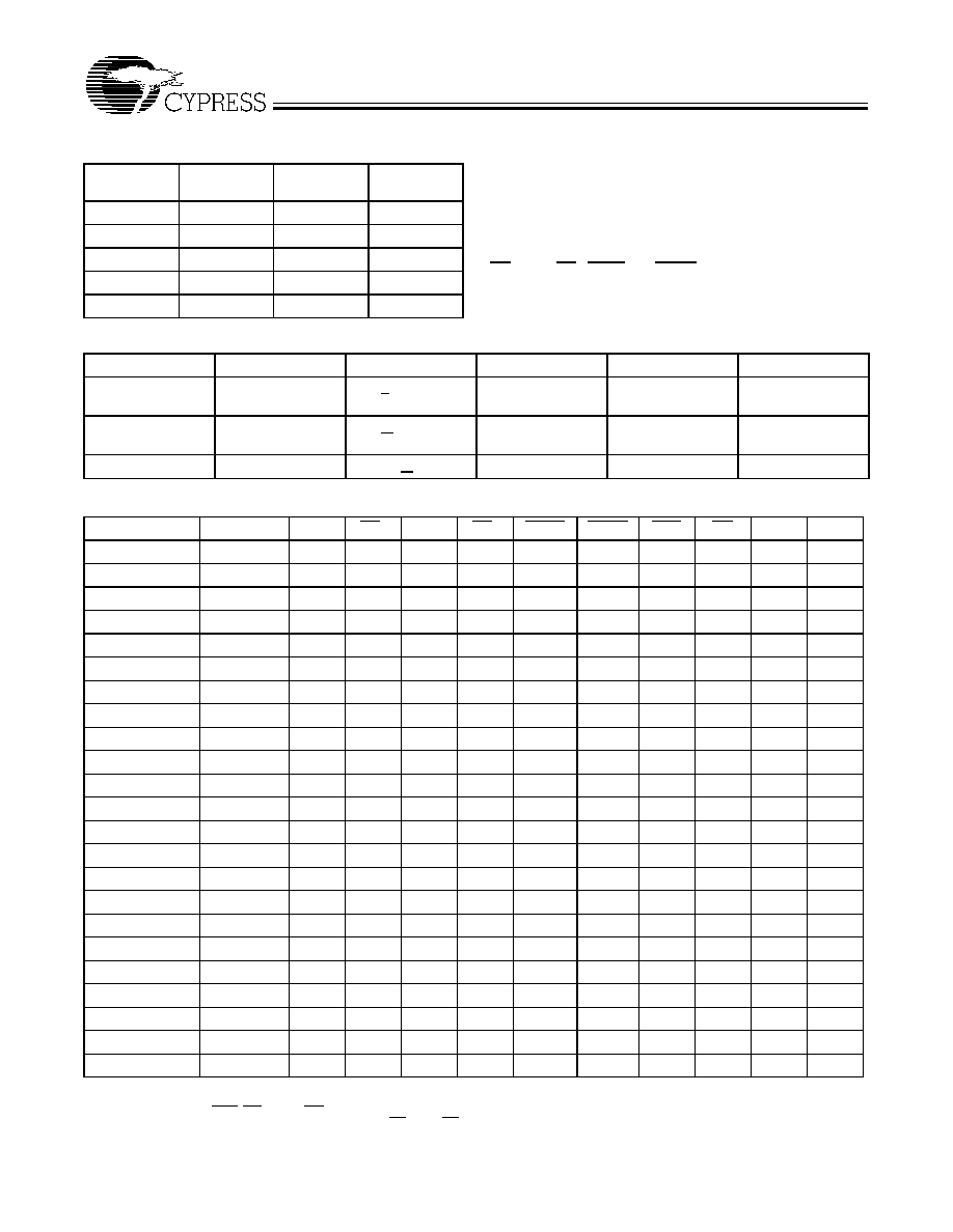
ZZ Mode Electrical Characteristics
Parameter
Description
Test Conditions
Min
Max
Unit
I
DDZZ
Snooze mode
standby current
ZZ > V
DD
-
0.2V
3
mA
t
ZZS
Device operation to
ZZ
ZZ > V
DD
-
0.2V
2t
CYC
ns
t
ZZREC
ZZ recovery time
ZZ < 0.2V
2t
CYC
ns
Cycle Descriptions
[1,2,3]
Next Cycle
Add. Used
ZZ
CE
3
CE
2
CE
1
ADSP
ADSC
ADV
OE
DQ
Write
Unselected
None
L
X
X
1
X
0
X
X
Hi-Z
X
Unselected
None
L
1
X
0
0
X
X
X
Hi-Z
X
Unselected
None
L
X
0
0
0
X
X
X
Hi-Z
X
Unselected
None
L
1
X
0
1
0
X
X
Hi-Z
X
Unselected
None
L
X
0
0
1
0
X
X
Hi-Z
X
Begin Read
External
L
0
1
0
0
X
X
X
Hi-Z
X
Begin Read
External
L
0
1
0
1
0
X
X
Hi-Z
read
Continue Read
Next
L
X
X
X
1
1
0
1
Hi-Z
read
Continue Read
Next
L
X
X
X
1
1
0
0
DQ
read
Continue Read
Next
L
X
X
1
X
1
0
1
Hi-Z
read
Continue Read
Next
L
X
X
1
X
1
0
0
DQ
read
Suspend Read
Current
L
X
X
X
1
1
1
1
Hi-Z
read
Suspend Read
Current
L
X
X
X
1
1
1
0
DQ
read
Suspend Read
Current
L
X
X
1
X
1
1
1
Hi-Z
read
Suspend Read
Current
L
X
X
1
X
1
1
0
DQ
read
Begin Write
Current
L
X
X
X
1
1
1
X
Hi-Z
write
Begin Write
Current
L
X
X
1
X
1
1
X
Hi-Z
write
Begin Write
External
L
0
1
0
1
0
X
X
Hi-Z
write
Continue Write
Next
L
X
X
X
1
1
0
X
Hi-Z
write
Continue Write
Next
L
X
X
1
X
1
0
X
Hi-Z
write
Suspend Write
Current
L
X
X
X
1
1
1
X
Hi-Z
write
Suspend Write
Current
L
X
X
1
X
1
1
X
Hi-Z
write
ZZ "sleep"
None
H
X
X
X
X
X
X
X
Hi-Z
X
Notes:
1.
X="Don't Care", 1=HIGH, 0=LOW.
2.
Write is defined by BWE, BW
[3:0]
, and GW. See Write Cycle Descriptions table.
3.
The DQ pins are controlled by the current cycle and the OE signal. OE is asynchronous and is not sampled with the clock.