13 Output, 3.3V SDRAM Buffer for
Desktop PCs with 3 DIMMs
CY2313ANZ
Cypress Semiconductor Corporation
À
3901 North First Street
À
San Jose
À
CA 95134
À
408-943-2600
Document #: 38-07144 Rev. *A
Revised December 14, 2002
0NZCY2310
13ANZ
Features
À One input to 13 output buffer/driver
À Supports up to three SDRAM DIMMs
À One additional outputs for feedback
À Serial interface for output control
À Low skew outputs
À Up to 100-MHz operation
À Multiple V
DD
and V
SS
pins for noise reduction
À Low EMI outputs
À 28-pin SOIC (300-mil) package
À 3.3V operation
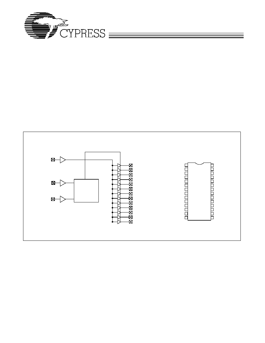
Functional Description
The CY2313ANZ is a 3.3V buffer designed to distribute
high-speed clocks in desktop PC applications. The part has 13
outputs, 12 of which can be used to drive up to three SDRAM
DIMMs, and the remaining can be used for external feedback
to a PLL. The device operates at 3.3V and outputs can run up
to 100 MHz, thus making it compatible with Pentium
«
II pro-
cessors. The CY2313ANZ can be used in conjunction with the
CY2280, CY2281, CY2282 or similar clock synthesizer for a
complete Pentium II motherboard solution.
The CY2313ANZ also includes a serial interface which can
enable or disable each output clock. On power-up, all output
clocks are enabled.
Pentium is a registered trademark of Intel Corporation.
Block Diagram
Serial Interface
BUF_IN
SDATA
SCLOCK
SDRAM0
SDRAM1
SDRAM2
SDRAM3
SDRAM4
SDRAM5
SDRAM6
SDRAM7
1
2
3
4
V
DD
SDRAM11
SDRAM10
V
SS
V
DD
SDRAM9
28 SOIC
Top View
Pin Configuration
Decoding
8
5
6
7
12
9
10
11
13
14
28
27
26
25
21
24
23
22
17
20
19
18
16
15
SDRAM8
V
SS
V
DD
SDRAM7
SDRAM6
V
SS
V
SSIIC
SCLK
V
DD
SDRAM0
SDRAM1
V
SS
V
DD
SDRAM2
V
SS
BUF_IN
SDRAM4
SDRAM5
SDRAM12
V
DDIIC
SDATA
SDRAM3
SDRAM8
SDRAM9
SDRAM10
SDRAM11
SDRAM12
CY2313ANZ
Document #: 38-07144 Rev. *A
Page 2 of 8
Serial Configuration Map
À The Serial bits will be read by the clock driver in the following
order:
Byte 0 - Bits 7, 6, 5, 4, 3, 2, 1, 0
Byte 1 - Bits 7, 6, 5, 4, 3, 2, 1, 0
.
Byte N - Bits 7, 6, 5, 4, 3, 2, 1, 0
À Reserved and unused bits should be programmed to "0"
À Serial interface address for the CY2313ANZ is:
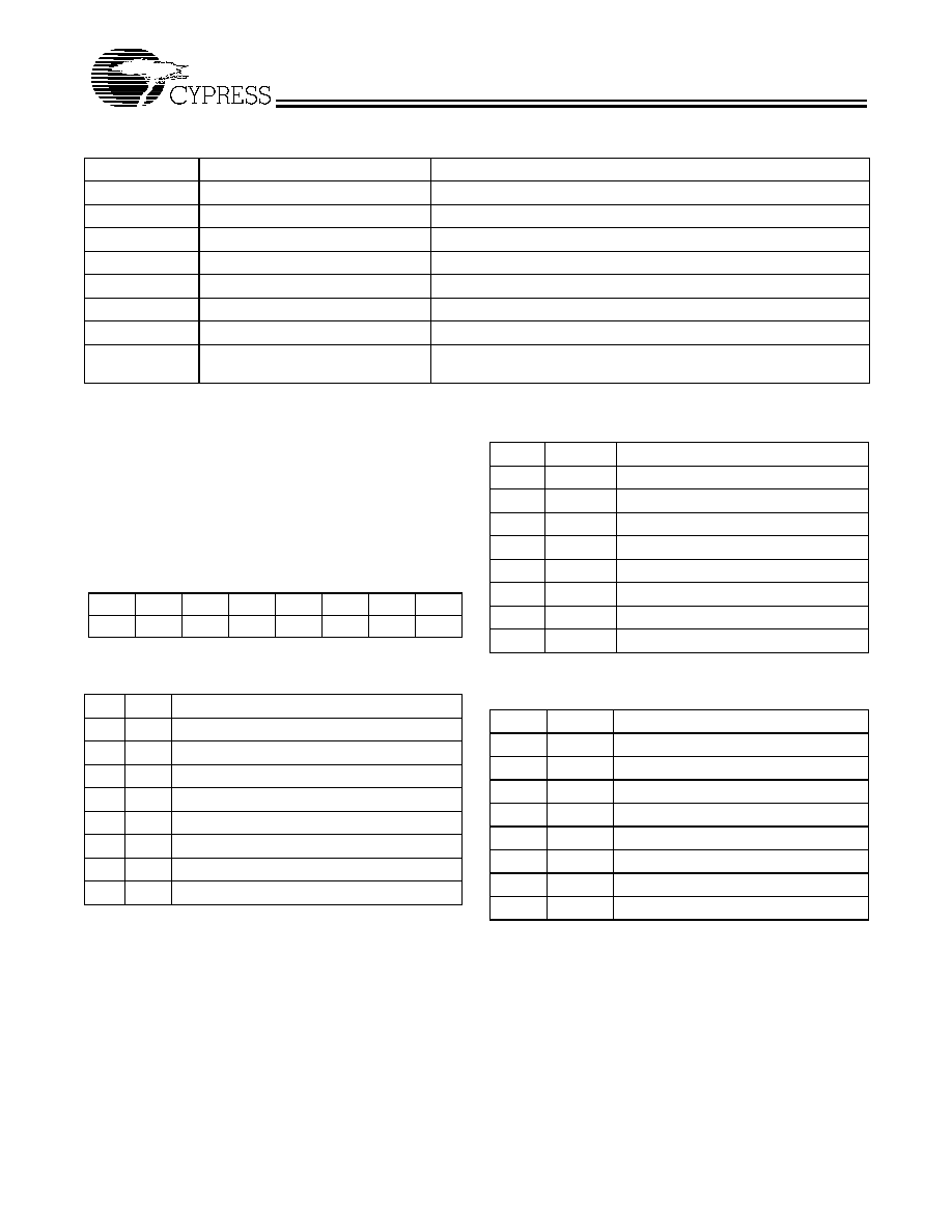
Pin Summary
Name
Pins
Description
V
DD
1, 5, 20, 24, 28
3.3V Digital voltage supply
V
SS
4, 8, 17, 21, 25
Ground
V
DDIIC
13
Serial interface voltage supply
V
SSIIC
16
Ground for serial interface
BUF_IN
9
Input clock
SDATA
14
Serial data input, internal pull-up to V
DD
SCLK
15
Serial clock input, internal pull-up to V
DD
SDRAM [0-12]
2, 3, 6, 7, 10, 11, 12, 18, 19, 22, 23,
26, 27
SDRAM clock outputs
A6
A5
A4
A3
A2
A1
A0
R/W
1
1
0
1
0
0
1
----
Byte 0:SDRAM Active/Inactive Register
(1 = Enable, 0 = Disable), Default = Enabled
Bit
Pin #
Description
Bit 7 11
SDRAM5 (Active/Inactive)
Bit 6 10
SDRAM4 (Active/Inactive)
Bit 5 --
Reserved, drive to 0
Bit 4 --
Reserved, drive to 0
Bit 3 7
SDRAM3 (Active/Inactive)
Bit 2 6
SDRAM2 (Active/Inactive)
Bit 1 3
SDRAM1 (Active/Inactive)
Bit 0 2
SDRAM0 (Active/Inactive)
Byte 1: SDRAM Active/Inactive Register
(1 = Active, 0 = Inactive), Default = Active
Bit
Pin #
Description
Bit 7
27
SDRAM11 (Active/Inactive)
Bit 6
26
SDRAM10 (Active/Inactive)
Bit 5
23
SDRAM9 (Active/Inactive)
Bit 4
22
SDRAM8 (Active/Inactive)
Bit 3
--
Reserved, drive to 0
Bit 2
--
Reserved, drive to 0
Bit 1
19
SDRAM7 (Active/Inactive)
Bit 0
18
SDRAM6 (Active/Inactive)
Byte 2: SDRAM Active/Inactive Register
(1 = Active, 0 = Inactive), Default = Active
Bit
Pin #
Description
Bit 7
--
Reserved, drive to 0
Bit 6
12
SDRAM12 (Active/Inactive)
Bit 5
--
Reserved, drive to 0
Bit 4
--
Reserved, drive to 0
Bit 3
--
Reserved, drive to 0
Bit 2
--
Reserved, drive to 0
Bit 1
--
Reserved, drive to 0
Bit 0
--
Reserved, drive to 0
CY2313ANZ
Document #: 38-07144 Rev. *A
Page 3 of 8
Maximum Ratings
Supply Voltage to Ground Potential ............... ¡0.5V to +7.0V
DC Input Voltage (Except BUF_IN)........¡0.5V to V
DD
+ 0.5V
DC Input Voltage (BUF_IN)............................ ¡0.5V to +7.0V
Storage Temperature ................................. ¡65
░
C to +150
░
C
Junction Temperature ................................................. 150
░
C
Static Discharge Voltage
(per MIL-STD-883, Method 3015) ............................. >2000V
Operating Conditions
[1]
Parameter
Description
Min.
Max.
Unit
V
DD
Supply Voltage
3.135
3.465
V
T
A
Operating Temperature (Ambient Temperature)
0
70
░
C
C
L
Load Capacitance
30
pF
C
IN
Input Capacitance
7
pF
t
PU
Power-up time for all VDD's to reach minimum specified voltage
(power ramps must be monotonic)
0.05
50
ms
Electrical Characteristics
Over the Operating Range
Parameter
Description
Test Conditions
Min.
Max.
Unit
V
IL
Input LOW Voltage
[2]
Except serial interface pins
0.8
V
V
ILiic
Input LOW Voltage
For serial interface pins only
0.7
V
V
IH
Input HIGH Voltage
[2]
2.0
V
I
IL
Input LOW Current
(BUF_IN input)
V
IN
= 0V
¡10
10
Á
A
I
IL
Input LOW Current
(Except BUF_IN Pin)
V
IN
= 0V
100
Á
A
I
IH
Input HIGH Current
V
IN
= V
DD
¡10
10
Á
A
V
OL
Output LOW Voltage
[3]
I
OL
= 25 mA
0.4
V
V
OH
Output HIGH Voltage
[3]
I
OH
= ¡36 mA
2.4
V
I
DD
Supply Current
[3]
Unloaded outputs, 100 MHz
200
mA
I
DD
Supply Current
[3]
Loaded outputs, 100 MHz
290
mA
I
DD
Supply Current
[3]
Unloaded outputs, 66.67 MHz
150
mA
I
DD
Supply Current
[3]
Loaded outputs, 66.67 MHz
185
mA
I
DDS
Supply Current
BUF_IN=V
DD
or V
SS
All other inputs at V
DD
500
Á
A
Notes:
1.
Electrical parameters are guaranteed under the operating conditions specified.
2.
BUF_IN input has a threshold voltage of V
DD
/2.
3.
Parameter is guaranteed by design and characterization. Not 100% tested in production.
CY2313ANZ
Document #: 38-07144 Rev. *A
Page 4 of 8
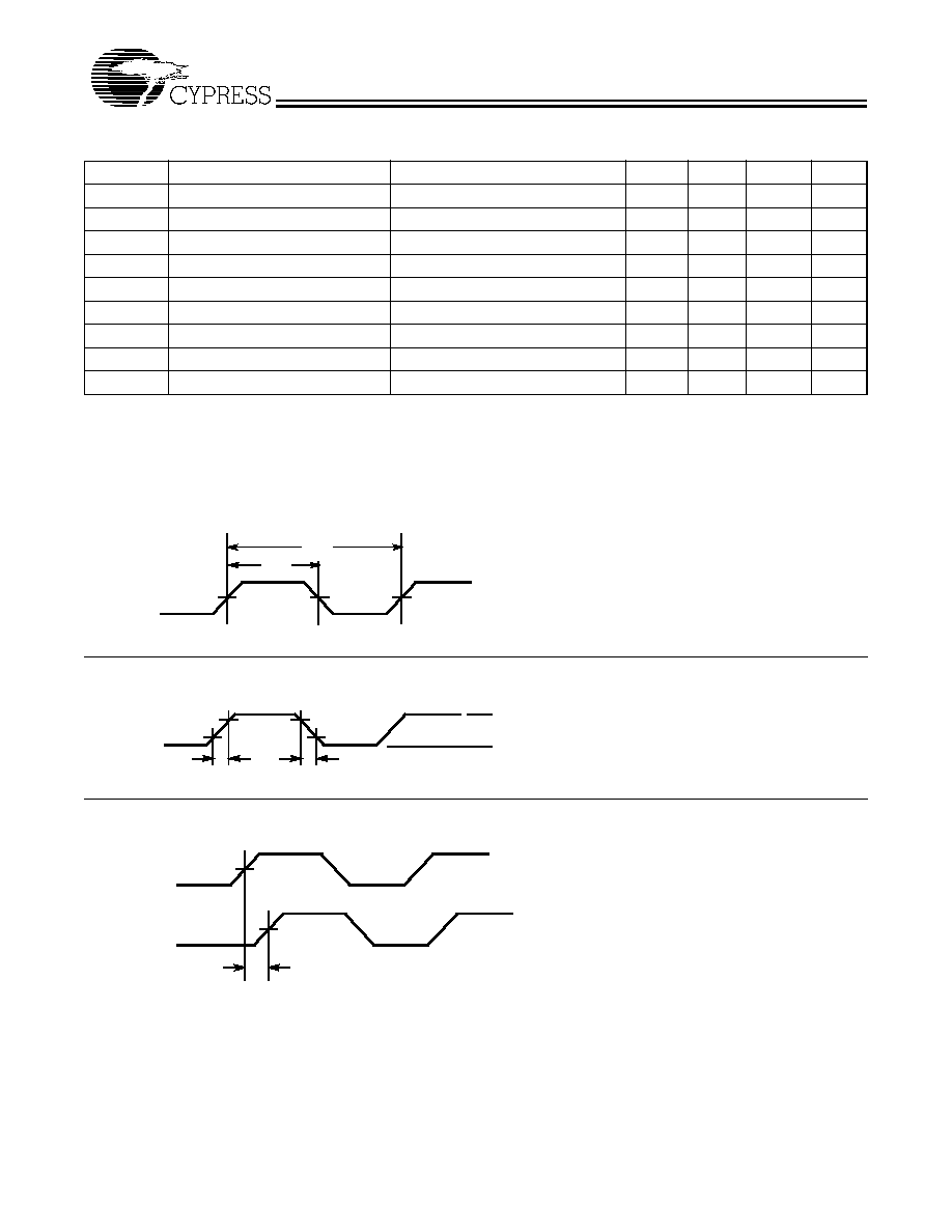
Switching Characteristics
[4]
Over the Operating Range
Parameter
Name
Test Conditions
Min.
Typ.
Max.
Unit
Maximum Operating Frequency
100
MHz
Duty Cycle
[3,5]
= t
2
¸
t
1
Measured at 1.5V
45.0
50.0
55.0
%
t
3
Rising Edge Rate
[3]
Measured between 0.4V and 2.4V
0.9
1.5
4.0
V/ns
t
4
Falling Edge Rate
[3]
Measured between 2.4V and 0.4V
0.9
1.5
4.0
V/ns
t
5
Output to Output Skew
[3]
All outputs equally loaded
¡250
+250
ps
t
6
SDRAM Buffer LH Prop. Delay
[3]
Input edge greater than 1 V/ns
1.0
3.5
5.0
ns
t
7
SDRAM Buffer HL Prop. Delay
[3]
Input edge greater than 1 V/ns
1.0
3.5
5.0
ns
t
8
SDRAM Buffer Enable Delay
[3]
Input edge greater than 1 V/ns
1.0
5
12
ns
t
9
SDRAM Buffer Disable Delay
[3]
Input edge greater than 1 V/ns
1.0
20
30
ns
Notes:
4.
All parameters specified with loaded outputs.
5.
Duty cycle of input clock is 50%. Rising and falling edge rate of the input clock is greater than 1 V/ns.
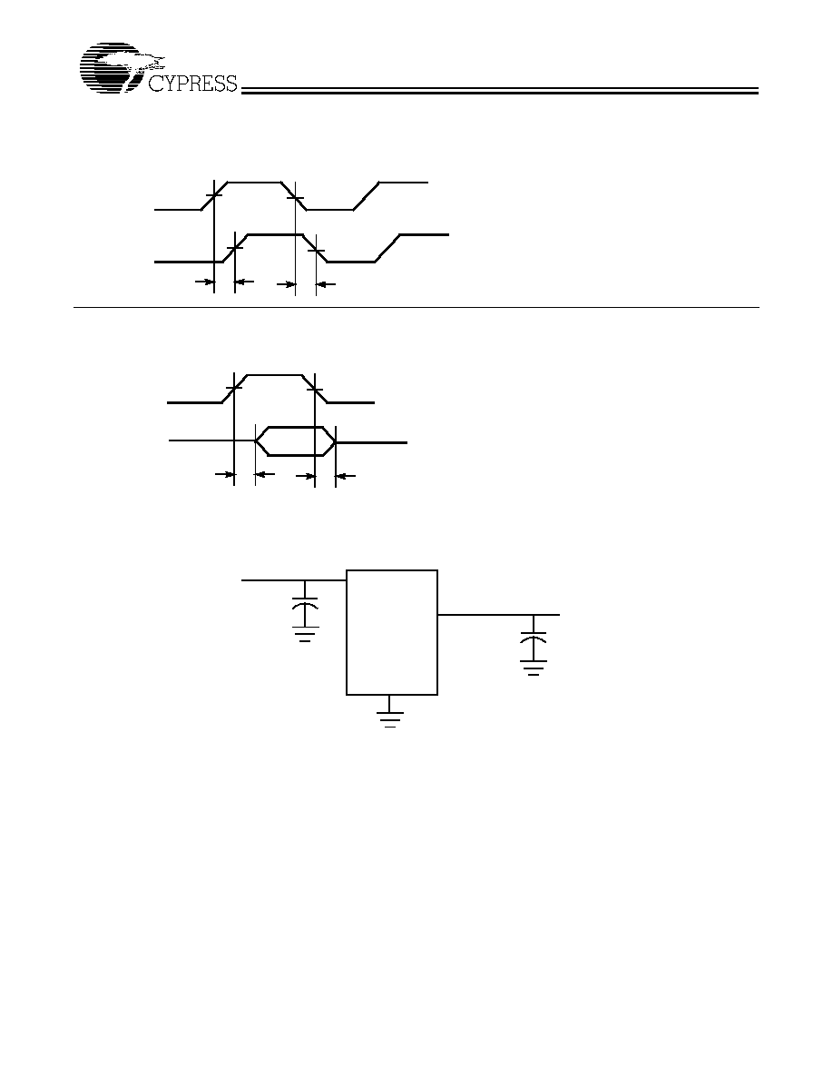
Switching Waveforms
Duty Cycle Timing
t
1
t
2
1.5V
1.5V
1.5V
All Outputs Rise/Fall Time
OUTPUT
t
3
3.3V
0V
0.4V
2.4V
2.4V
0.4V
t
4
Output-Output Skew
1.5V
t
5
OUTPUT
OUTPUT
1.5V
CY2313ANZ
Document #: 38-07144 Rev. *A
Page 5 of 8
Switching Waveforms
(continued)
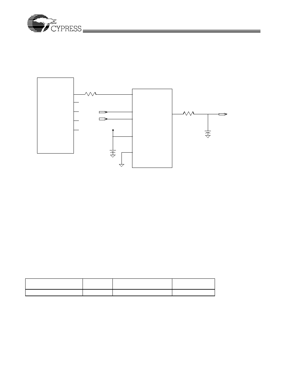
SDRAM Buffer LH and HL Propagation Delay
t
6
INPUT
OUTPUT
t
7
t
8
OE
OUTPUTS
SDRAM Buffer Enable and Disable Times
t
9
Three-State
Active
0.1
Á
F
V
DD
CLK out
C
LOAD
OUTPUTS
GND
Test Circuit
CY2313ANZ
Document #: 38-07144 Rev. *A
Page 6 of 8
Application Information
Clock traces must be terminated with either series or parallel termination, as is normally done.
Summary
À Surface mount, low-ESR, ceramic capacitors should be used for filtering. Typically, these capacitors have a value of 0.1
Á
F.
In some cases, smaller value capacitors may be required.
À The value of the series terminating resistor satisfies the following equation, where Rtrace is the loaded characteristic impedance
of the trace, Rout is the output impedance of the buffer (typically 25
), and Rseries is the series terminating resistor.
Rseries > Rtrace ¡ Rout
À Footprints must be laid out for optional EMI-reducing capacitors, which should be placed as close to the terminating resistor
as is physically possible. Typical values of these capacitors range from 4.7 pF to 22 pF.
À A Ferrite Bead may be used to isolate the Board V
DD
from the clock generator V
DD
island. Ensure that the Ferrite Bead offers
greater than 50
impedance at the clock frequency, under loaded DC conditions. Please refer to the application note "Layout
and Termination Techniques for Cypress Clock Generators" for more details.
À If a Ferrite Bead is used, a 10
Á
F¡22
Á
F tantalum bypass capacitor should be placed close to the Ferrite Bead. This capacitor
prevents power supply droop during current surges.
Application Circuit
C
d
= DECOUP LING CAPACITOR S
C
t
= OPTIONAL EMI-R EDUCING CAP ACI TORS
R
s
= SERIES TERMINATING RESISTORS
* CY2280 48 PIN SSOP
(or CY2281 or CY2282)
CY2313 28 PIN SOIC
C
d
0.1uF
V
DD
3.3V
V
SS
BUF_IN
V
DD
C
t
SDRAM ( 0-12)
SDRAM ( 0-12)
SDATA
SCLK
R
s
SDATA
SCLK
CPUCLK
PCICLK
USBCLK
REF
APIC
R
s
* THIS FREQUENCY SYNTHESIZER IS USED TO
GENERATE CPU, PCI, USB, REF, AND APIC CLOCKS.
CY2313A: 28-PIN SOIC
Ordering Information
Ordering Code
Package
Name
Package Type
Operating
Range
CY2313ANZSC¡1
S21
28-Pin SOIC
Commercial
CY2313ANZ
Document #: 38-07144 Rev. *A
Page 7 of 8
® Cypress Semiconductor Corporation, 2001. The information contained herein is subject to change without notice. Cypress Semiconductor Corporation assumes no responsibility for the use
of any circuitry other than circuitry embodied in a Cypress Semiconductor product. Nor does it convey or imply any license under patent or other rights. Cypress Semiconductor does not authorize
its products for use as critical components in life-support systems where a malfunction or failure may reasonably be expected to result in significant injury to the user. The inclusion of Cypress
Semiconductor products in life-support systems application implies that the manufacturer assumes all risk of such use and in doing so indemnifies Cypress Semiconductor against all charges.
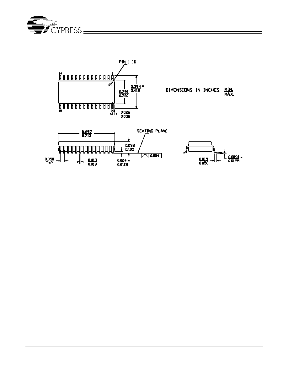
Package Diagram
28-Lead (300-Mil) Molded SOIC S21
51-85026-A

CY2313ANZ
Document #: 38-07144 Rev. *A
Page 8 of 8
Document Title: CY2313ANZ 13 Output, 3.3V SDRAM Buffer for Desktop PCs with 3 DIMMs
Document Number: 38-07144
REV.
ECN NO.
Issue
Date
Orig. of
Change
Description of Change
**
110253
11/18/01
DSG
Change from Spec number: 38-00692 to 38-07144
*A
121831
12/14/02
RBI
Power up requirements added to Operating Conditions Information