BC213143A-ds-001Pf
Production Information
© Copyright CSR 2003
This material is subject to CSR's non-disclosure agreement.
Device Features
_äěÉ`çęÉ
»
OJolj
Single Chip Bluetooth
®
System
Production Information Data Sheet for
BC213143A
Fully qualified Bluetooth system
Low power 1.8V operation
Minimum external components
Integrated 1.8V regulator
UART Bypass mode
Available in VFBGA and CSP packages
Available in `RF Plug and Go' package (see
separate data sheet)
June 2003
General Description
Applications
_äěÉ`çęÉOJolj=is a single chip radio and
baseband chip for Bluetooth wireless technology
2.4GHz systems.
It is implemented in 0.18
µm CMOS technology.
BlueCore2-ROM has the same pinout and
electrical characteristics as available in
BlueCore2-Flash to enable development of
custom code before committing to ROM.
The 4Mbit ROM is metal programmable, which
enables a six week turn-around from approval of
firmware to production samples.
Cellular Handsets
Personal Digital Assistants
Mice
Keyboards
High volume, cost sensitive production
BlueCore2-ROM has been designed to reduce the number
of external components required which ensures
production costs are minimised.
The device incorporates auto-calibration and built-in-self-
test (BIST) routines to simplify development, type approval
and production test. All hardware and device firmware is
fully compliant with the Bluetooth specification v1.1.
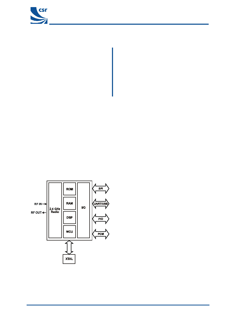
System Architecture

Contents
BC213143A-ds-001Pf
Production Information
© Copyright CSR 2003
This material is subject to CSR's non-disclosure agreement.
Page 2 of 50
_äěÉ`çęÉ
OÓolj=
Product Data Sheet
Contents
1
Key Features .................................................................................................................................................. 5
2
6 x 6 VFBGA Package Information ............................................................................................................... 6
2.1
BC213143AXX-EK and BC213143AXX-RK Pinout Diagram................................................................ 6
2.2
Device Terminal Functions ................................................................................................................... 7
3
4 x 4 CSP Package Information .................................................................................................................. 10
3.1
BC213143AXX-XB Pinout Diagram .................................................................................................... 10
3.2
Device Terminal Functions ................................................................................................................. 11
4
Electrical Characteristics ............................................................................................................................ 14
5
Radio Characteristics .................................................................................................................................. 19
5.1
Temperature +20°C ............................................................................................................................ 19
5.1.1
Transmitter ............................................................................................................................ 19
5.1.2
Receiver ................................................................................................................................ 20
5.1.3
Blocking................................................................................................................................. 21
5.2
Temperature -40°C ............................................................................................................................. 22
5.2.1
Transmitter ............................................................................................................................ 22
5.2.2
Receiver ................................................................................................................................ 22
5.3
Temperature -25°C ............................................................................................................................. 23
5.3.1
Transmitter ............................................................................................................................ 23
5.3.2
Receiver ................................................................................................................................ 23
5.4
Temperature +85°C ............................................................................................................................ 24
5.4.1
Transmitter ............................................................................................................................ 24
5.4.2
Receiver ................................................................................................................................ 24
5.5
Temperature +105°C .......................................................................................................................... 25
5.5.1
Transmitter ............................................................................................................................ 25
5.5.2
Receiver ................................................................................................................................ 25
5.6
Power Consumption ........................................................................................................................... 26
6
Device Diagrams .......................................................................................................................................... 27
7
Description of Functional Blocks ............................................................................................................... 28
7.1
RF Receiver........................................................................................................................................ 28
7.1.1
Low Noise Amplifier............................................................................................................... 28
7.1.2
Analogue to Digital Converter ............................................................................................... 28
7.2
RF Transmitter.................................................................................................................................... 28
7.2.1
IQ Modulator ......................................................................................................................... 28
7.2.2
Power Amplifier ..................................................................................................................... 28
7.2.3
Auxiliary DAC ........................................................................................................................ 28
7.3
RF Synthesiser ................................................................................................................................... 28
7.4
Clock Input and Generation ................................................................................................................ 28
7.5
Baseband and Logic ........................................................................................................................... 29
7.5.1
Memory Management Unit .................................................................................................... 29
7.5.2
Burst Mode Controller ........................................................................................................... 29
7.5.3
Physical Layer Hardware Engine DSP .................................................................................. 29
7.5.4
RAM ...................................................................................................................................... 29
7.5.5
ROM...................................................................................................................................... 29
7.5.6
USB....................................................................................................................................... 29
7.5.7
Synchronous Serial Interface ................................................................................................ 29
7.5.8
UART .................................................................................................................................... 29
7.5.9
Audio PCM Interface ............................................................................................................. 29
7.6
Microcontroller .................................................................................................................................... 30
7.6.1
Programmable I/O................................................................................................................. 30
8
CSR Bluetooth Software Stacks ................................................................................................................. 31
8.1
Important Information.......................................................................................................................... 31
8.2
BlueCore HCI Stack............................................................................................................................ 31
8.2.1
Key Features of the HCI Stack.............................................................................................. 32
8.3
BlueCore RFCOMM Stack.................................................................................................................. 34
8.3.1
Key Features of the BlueCore2-ROM RFCOMM Stack......................................................... 34

Contents
BC213143A-ds-001Pf
Production Information
© Copyright CSR 2003
This material is subject to CSR's non-disclosure agreement.
Page 3 of 50
_äěÉ`çęÉ
OÓolj=
Product Data Sheet
8.4
BlueCore Virtual Machine Stack ......................................................................................................... 35
8.5
BlueCore HID Stack............................................................................................................................ 36
8.6
Host Side Software ............................................................................................................................. 37
8.7
Additional Software for Other Embedded Applications ....................................................................... 37
8.8
CSR Development Systems ............................................................................................................... 37
9
Application Schematics............................................................................................................................... 38
9.1
6 x 6 VFBGA 84-Ball Package............................................................................................................ 38
9.1.1
Application Schematic using Separate Balun and Filter ........................................................ 38
9.1.2
Application Schematic using Epcos Combined Balun and Filter ........................................... 39
9.1.3
Application Schematic using Soshin Combined Balun and Filter .......................................... 40
9.2
4 x 4 CSP 49-Ball Package................................................................................................................. 41
10
Package Dimensions ................................................................................................................................... 42
10.1
6 x 6 VFBGA 84-Ball Package............................................................................................................ 42
10.2
4 x 4 CSP 47-Ball Package................................................................................................................. 43
11
Ordering Information ................................................................................................................................... 44
11.1
BlueCore2-ROM ................................................................................................................................. 44
12
Contact Information ..................................................................................................................................... 45
13
Document References ................................................................................................................................. 46
Acronyms and Definitions.................................................................................................................................. 47
Status Information .............................................................................................................................................. 49
Record of Changes ............................................................................................................................................. 50

Contents
BC213143A-ds-001Pf
Production Information
© Copyright CSR 2003
This material is subject to CSR's non-disclosure agreement.
Page 4 of 50
_äěÉ`çęÉ
OÓolj=
Product Data Sheet
List of Figures
Figure 6.1: BlueCore2-ROM Device Diagram for 6 x 6mm VFBGA and 4 x 4mm CSP Packages ....................... 27
Figure 8.1: BlueCore HCI Stack ............................................................................................................................ 31
Figure 8.2: BlueCore RFCOMM Stack .................................................................................................................. 34
Figure 8.3: Virtual Machine ................................................................................................................................... 35
Figure 8.4: HID Stack............................................................................................................................................ 36
Figure 9.1: Application Circuit using Separate Balun and Filter for 6 x 6 VFBGA Package .................................. 38
Figure 9.2: Application Circuit using Epcos Balun and Filter for 6 x 6 VFBGA Package ....................................... 39
Figure 9.3: Application Circuit using Soshin Balun and Filter for 6 x 6 VFBGA Package ...................................... 40
Figure 9.4: Application Circuit for 4 x 4 CSP Package .......................................................................................... 41
Figure 10.1: BlueCore2-ROM VFBGA Package Dimensions................................................................................ 42
Figure 10.2: BlueCore2-ROM CSP Package Dimensions..................................................................................... 43

Key Features
BC213143A-ds-001Pf
Production Information
© Copyright CSR 2003
This material is subject to CSR's non-disclosure agreement.
Page 5 of 50
_äěÉ`çęÉ
OÓolj=
Product Data Book
1 Key Features
Radio
Operation with common TX/RX terminals
simplifies external matching circuitry and
eliminates external antenna switch
Extensive built-in-self-test minimises
production test time
No external trimming is required in
production
Full RF reference designs are available
Transmitter
Up to +6dBm RF transmit power with level
control from the on-chip 6-bit DAC over a
dynamic range greater than 30dB
Supports Class 2 and Class 3 radios without
the need for an external power amplifier or
TX/RX switch
Supports Class 1 radios with an external
power amplifier, provided by a power control
terminal controlled by an internal 8-bit
voltage DAC and an external RF TX/RX
switch
Receiver
Integrated channel filters
Digital demodulator for improved sensitivity
and co-channel rejection
Digitised RSSI available in real time over the
HCI interface
Fast AGC for enhanced dynamic range
Synthesiser
Fully integrated synthesizer; no external
VCO varactor diode, resonator or loop filter
Compatible with crystals between 8 and
32MHz (in multiples of 250kHz) or an
external clock
Accepts 7.68, 14.4, 15.36, 16.2, 16.8, 19.2,
19.44, 19.68, 19.8 and 38.4MHz TCXO
frequencies for GSM and CDMA devices
with either sinusoidal or logic level signals
Auxiliary Features
Crystal oscillator with built-in digital trimming
Power management includes digital shut
down and wake up commands and an
integrated low power oscillator for ultra low
Park/Sniff/Hold mode power consumption
Device can be used with an external master
oscillator and provides a `clock request
signal' to control external clock source
Auxiliary Features
On-chip linear regulator, producing 1.8V output
from 2.2 4.2V input
Power on reset cell detects low supply voltage
Arbitrary sequencing of power supplies is
permitted
Uncommitted 8-bit ADC and 8-bit DAC are
available to application programs
Baseband and Software
Internal programmed 4Mbit ROM for complete
system solution
32Kbyte on-chip RAM allows full speed
Bluetooth data transfer, mixed voice and data,
plus full seven Slave piconet operation
Dedicated logic for forward error correction,
header error control, access code correlation,
demodulation, cyclic redundancy check,
encryption bitstream generation, whitening and
transmit pulse shaping
Transcoders for A-law,
µ-law and linear voice
from host and A-law,
µ-law and CVSD voice
over air
Physical Interfaces
Synchronous serial interface up to 4M Baud for
system debugging
UART interface with programmable Baud rate
up to 1.5M Baud with an optional bypass mode
Full speed USB interface supports OHCI and
UHCI host interfaces. Compliant with USB v2.0
Synchronous bi-directional serial
programmable audio interface
Optional I
2
C
TM
compatible interface
Bluetooth Stack
CSR's Bluetooth Protocol Stack runs on-chip in a
variety of configurations:
Standard HCI (UART or USB)
Fully embedded to RFCOMM
Customer specific builds with embedded
application code
Package Options
84-ball VFBGA 6 x 6 x 1.0mm 0.5mm pitch
49-ball CSP 4 x 4 x 0.7mm 0.5mm pitch