Rev 2
UPF14060
UPF14060
60W, 1.66 GHz, 26V Broadband RF Power N-Channel
Enhancement-Mode Lateral MOSFET
Designed for DCS base station applications at 1400 MHz. Rated with a minimum output power
of 60W, it is ideal for 16 QAM, CDMA, TDMA, GSM, and Multi-Carrier Power Amplifiers in
Class A or AB operation.
Or
�
�
�
�
All Gold Metal system for highest reliability
Industry standard package
Internally matched for repeatable manufacturing
High gain, high efficiency and high linearity
Application Specific Performance (Typical, 1.4 GHz
GSM:
60 Watts
13.5 dB
EDGE:
25 Watts
13 dB
IS95 CDMA
7.5 Watts
13 dB
W-CDMA:
5 Watts 13 dB
16 QAM
35 Watts
13.5dB
�
Typical Edge Performance
(ETSI 300-910 GSM 05.05 v. 5.5.1)
Average Load Power
25W
PAE 30%
Power
Gain
13
dB
ACPR1
57
dBc
(30 kHz BW offset � 400 kHz normalized to total
power in a 30 kHz BW)
ACPR2
66
dBc
(30 kHz BW offset � 600 kHz normalized to total
power in a 30 kHz BW)
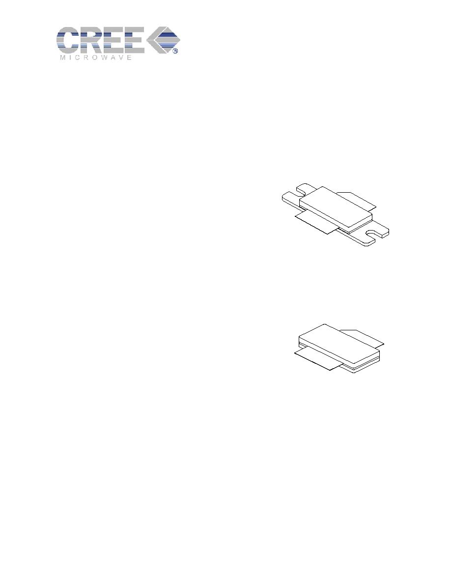
Package Type 440133
PN: UPF14060P
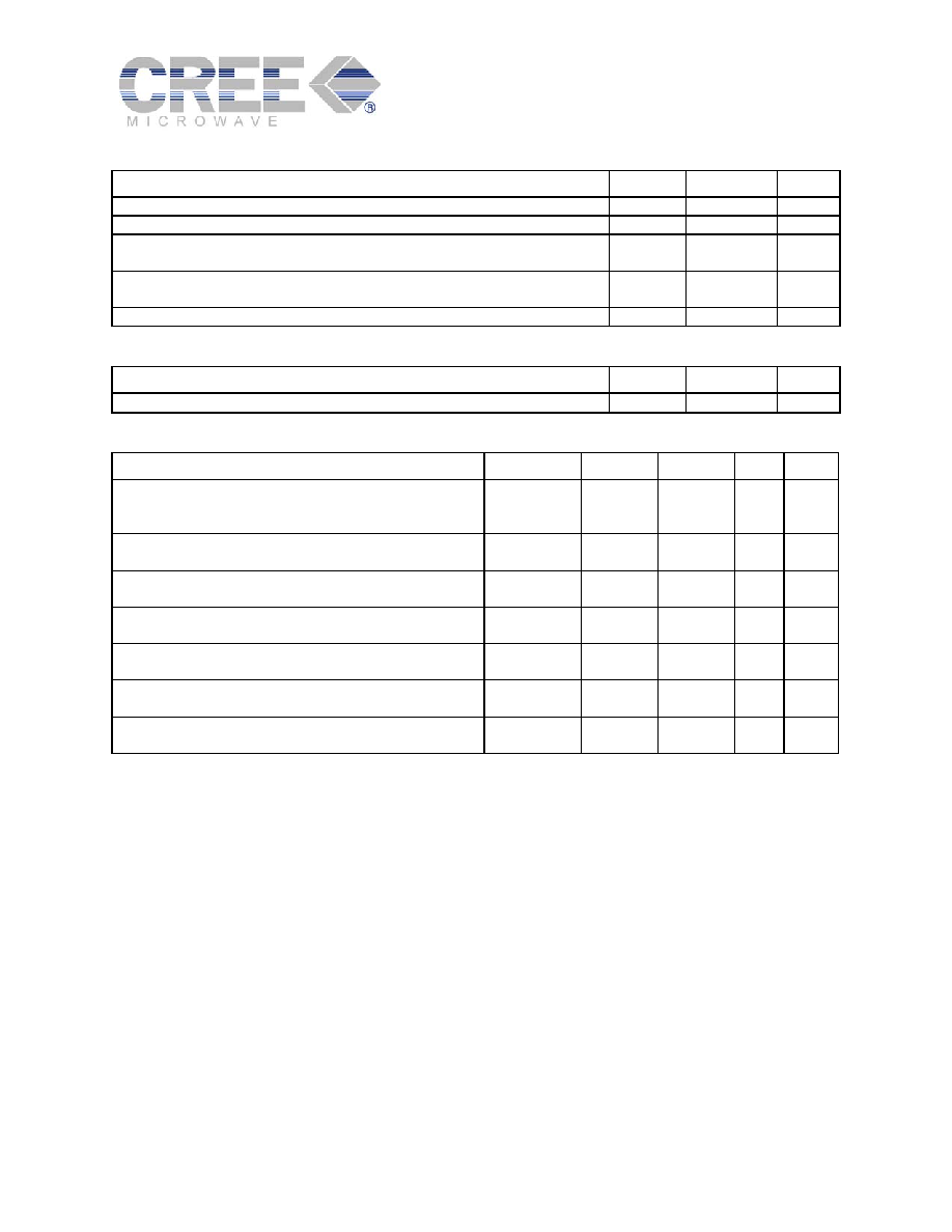
Package Type 440171
PN: UPF14060F
Rev 2
UPF14060
UPF14060
Maximum Ratings
Rating Symbol
Value
Unit
Drain to Source Voltage, Gate connected to Source
BV
DSS
65 Volts
Gate to Source Voltage
BV
GSS
+15/-0.5 Volts
Total Device Dissipation @ TC = 70
o
C
Derate above 70
o
C
P
D
100
0.8
Watts
W/
o
C
Storage Temperature Range
T
stg
-65 to
+150
o
C
Operating Junction Temperature
T
J
200
o
C
Thermal Characteristics
Characteristic Symbol
Typical
Unit
Thermal Resistance, Junction to Case
JC
0.97
o
C/W
Electrical DC Characteristics
(T
C
=25
�C unless otherwise specified)
Rating Symbol
Min
Typ
Max
Unit
Drain to Source Voltage,
Gate connected to source
(V
GS
=0, I
D
=1mA)
BV
DSS
65 - -
Volts
Drain to Source Leakage current
(V
DS
=26V, V
GS
=0)
I
DSS
- -
2.0
mA
Gate to Source Leakage current
(V
GS
=15V, V
DS
=0)
I
GSS
- -
2.0
�A
Threshold Voltage
(V
DS
=10V, I
D
=1mA)
V
TH
- 3.5
-
Volts
Gate Quiescent Voltage
(V
DS
=26 V, I
D
=540mA)
V
GS(on)
3.0 4.0
5.0
Volts
Drain to Source On Voltage
(V
GS
=10V, I
D
=1A)
V
DS(on)
- 0.14
-
Volts
Forward Transconductance
(V
DS
=10V, I
D
=5A)
Gm - 3.0
-
S

Rev 2
UPF14060
UPF14060
AC Characteristics
(T
C
=25
�C unless otherwise specified)
Rating Symbol
Min
Typ
Max
Unit
Input Capacitance *
(V
DS
=26V, V
GS
=0V, freq= 1MHz)
C
ISS
- - -
pF
Output capacitance *
(V
DS
= 26V, V
GS
=0V, freq = 1MHz)
C
OSS
- 52 -
pF
Feedback capacitance *
(V
DS
=26V, V
GS
=0V, freq = 1MHz)
C
RSS
- 3.0 -
pF
* Part is internally matched.
RF and Functional Tests
(Tc=25
�C unless otherwise specified, Cree Microwave Broadband Fixture
Rating Symbol
Min
Typ
Max
Unit
Two-Tone Common-Source Amplifier
Power Gain
(V
DD
=26V, I
DQ
=540mA, P
out
= 60W PEP
f
1
=1400 MHz and 1400.1 MHz,
G
ps
12.0 13 - dB
Two-Tone Drain Efficiency
(V
DD
=26V, P
out
= 60W PEP, I
DQ
=540mA
Freq=1400 MHz and 1400.1 MHz
- 35 -
%
P
out
= 1dB Compression Point
(V
DD
=26V, P
out
= 60W CW, f = 1400 MHz
P1db 60 -
- W
Input Return Loss
(V
DD
=26V, P
out
= 60W PEP, I
DQ
=540mA
f
1
=1400 MHz and 1400.1 MHz
IRL - -12 -
dB
Load Mismatch Tolerance
(V
DS
=26V, I
DQ
=540mA, Pout=60W, f=1400 MHz)
VSWR 10:1
-
-
Note (unless otherwise specified):
1. Source and load impedance shall be 50 ohms.
*No degradation in device performance after test.
CAUTION - MOS Devices are susceptible to damage from Electrostatic Discharge (ESD). Appropriate
precautions in handling, packaging and testing MOS devices must be observed.

Rev 2
UPF14060
UPF14060
Package Dimensions
Package Number 440171
Package Number 440133