
UGF2005 Rev. 2.
UGF2005
5W, 2.0 GHz, 26V Broadband RF Power N-Channel
Enhancement-Mode Lateral MOSFET
Designed for PCS base station applications in the frequency band 1.93 to 1.99 GHz. Rated
with a minimum output power of 5W, it is ideal for CDMA, TDMA, GSM, and Multi-Carrier
Power Amplifiers in Class A or AB operation.
·
·
·
·
ALL GOLD metal system for highest reliability
Industry standard package
High gain, high efficiency and high linearity
Application Specific Performance, 1.99 GHz
GSM:
5 Watts
15 dB
EDGE:
2.5 Watts
15 dB
IS95 CDMA:
1 Watt
15 dB
W-CDMA:
0.5 Watt
15 dB
Package Type 440095
PN: UGF2005F
Package Type 440109
PN: UGF2005P
Package Type 440178
PN: UGF2005-178
UGF2005 Rev. 2.
UGF2005
Maximum Ratings
Rating Symbol
Value
Unit
Drain to Source Voltage, gate connected to source
BVdss
65
Volts
Gate to Source Voltage
BVgss
+15 to -0.5
Volts
Total Device Dissipation @ Tcase = 70
o
C
Derate above 70
o
C
Pd
16.0
0.13
Watts
W/
o
C
Storage Temperature Range
Tstg
-65 to +150
o
C
Operating Junction Temperature
Tj
200
o
C
Thermal Characteristics
Characteristics Symbol
Typical
Unit
Thermal Resistance, Junction to Case
jc
8.0
o
C/W
Electrical DC Characteristics
(Tc=25
o
C unless otherwise specified)
Rating Symbol
Min
Typ
Max
Unit
Drain to Source Voltage, gate connected to source
(V
GS
=0, I
DS
=1mA)
BV
DSS
65 - -
Volts
Drain to Source Leakage current
(V
DS
=26V, V
GS
=0)
I
DSS
- -
10
µ
A
Gate to Source Leakage current
(V
GS
=20V, V
DS
=0)
I
DSS
- -
1.0
µ
A
Threshold Voltage
(V
DS
=10V, I
DS
=1mA)
Vth 2.0
3.5
5.0
Volts
Gate Quiescent Voltage
(V
DS
=26 V, I
DS
=53mA)
V
GS
(on) 3.0 4.0 6.0
Volts
Drain to Source On Voltage
(V
GS
=10V, I
DS
=0.2A
V
DS
(on) - 1.7
1.9
Volts
UGF2005 Rev. 2.
UGF2005
AC Characteristics
(Tc=25
o
C unless otherwise specified)
Rating Symbol
Min
Typ
Max
Unit
Input Capacitance
(V
DS
=19V, V
GS
=0, freq= 1MHz)
C
ISS
- 3.3 -
pF
Output capacitance
(V
DS
= 26V, V
GS
=0V, freq= 1MHz)
C
OSS
- 6.3 -
pF
Feedback capacitance
(V
DS
=26V, V
GS
=0V, freq= 1MHz
C
RSS
- 0.1 -
pF
RF and Functional Tests
(Tc=25
o
C unless otherwise specified, Cree Microwave Broadband Fixture)
Rating Symbol
Min
Typ
Max
Unit
Linear Power Gain, Single tone
(V
DS
=26V, I
DQ
=53mA, P
OUT
=1W, f=1990 MHz)
G
L
13.5 15 -
dB
Compressed Power Gain, Single tone
(V
DS
=26V, I
DQ
=53mA, P
OUT
=5W, f=1990 MHz)
G
P
13 14.5 -
dB
Drain Efficiency, Single Tone
(V
DS
=26V, I
DQ
=53mA, P
OUT
=5W, f=1990 MHz)
D
42 48 -
%
Intermodulation Distortion, Two Tone
(V
DS
=26V, I
DQ
=53mA, P
OUT
=5W PEP
f1=1990 MHz, f2=1990.1MHz)
IMD - -32 -30
dBc
Load Mismatch Tolerance
(V
DS
=26V, I
DQ
=53mA, P
OUT
=5W, f=1930 MHz)
VSWR* 10:1
-
-
Note (unless otherwise specified):
1. Source and load impedance shall be 50 ohms.
*No degradation in device performance after test.
CAUTION - MOS Devices are susceptible to damage from Electrostatic Discharge (ESD). Appropriate
precautions in handling, packaging and testing MOS devices must be observed.

UGF2005 Rev. 2.
UGF2005
UGF2005 Gain Vs. Frequency @ 5 W
14
14.2
14.4
14.6
14.8
15
15.2
15.4
1900
1920
1940
1960
1980
2000
Frequency [MHz]
Gain [dB]
Pg(dB)
Vdd = 26V,
IDQ = 53 mA
Pout = 37dBm
UGF2005 CW Efficiency Vs. Output Power
@1960 MHz
10
20
30
40
50
60
25
27
29
31
33
35
37
Output Power [dBm]
Efficiency [%]
Efficiency
Vdd = 26V
IDQ = 53 mA
UGF2005 Rev. 2.
UGF2005
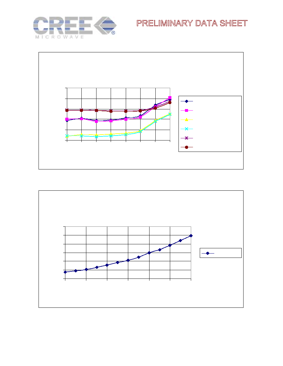
UGF2005 IS-95 CDMA ACPR Vs. Average
Output Power @ 1960 MHz
-70
-65
-60
-55
-50
-45
23
24
25
26
27
28
29
30
Average Output Power [dBm]
ACPR [dBc]
ACPR-(885KHz)
ACPR+(885KHz)
ACPR-(1.25MHz)
ACPR+(1.25MHz)
ACPR-(2.25MHz)
ACPR+(2.25MHz)
Vdd = 26V
IDQ = 53 mA
Gp = 15 dB
UGF2005 IS95 Efficiency Vs. Average Output
Power @ 1960 MHz
0
5
10
15
20
25
30
18
20
22
24
26
28
30
Average Output Power [dBm]
Efficiency [%]
Efficiency
Vdd = 26V
IDQ = 53 mA
Gp = 15 dB