
Preliminary Product Information
This document contains information for a new product.
Cirrus Logic reserves the right to modify this product without notice.
1
Copyright
Cirrus Logic, Inc. 2000
(All Rights Reserved)
P.O. Box 17847, Austin, Texas 78760
(512) 445 7222 FAX: (512) 445 7581
http://www.cirrus.com
CS5541
Low-Power, Low-Voltage, 24-Bit
ADC
Features
l
Analog-to-Digital Converter
- Linearity Error: 0.0015% FS
- RMS Noise: 2
µV
l
Two Channel Differential MUX
l
Buffered, Fully Differential Analog and
Voltage Reference Inputs
l
Scalable V
REF
Input: 0.1 V to Analog Supply
l
Absolute Accuracy via Calibration
l
Flexible Digital Filters
- Single Conversion Settling at 13.4 SPS or 4
Conversion Settling at 53.7 SPS with
Simultaneous 50/60 Hz Rejection
- Single Conversion Settling at 64.8 SPS or Four
Conversion Settling at 260 SPS with 16-bit
Resolution
l
Simple 3-Wire Serial Interface
- SPI
TM
and Microwire
TM
Compatible
- Schmitt Trigger on Serial Clock (SCLK)
l
Low Power
- Single +3.0 V Supply
- 330
µA Operating; 10 µA Sleep Current
Description
The CS5541 is a 24-bit low-power and low-voltage
analog-to-digital converter (ADC). It is optimized to con-
vert analog signals in DC measurement applications,
such as temperature and pressure measurement, and
various portable devices where low-power consumption
is required.
To accommodate these applications, the ADC integrates
analog input and reference buffers for increased input
impedance and includes a two-channel multiplexer. Ab-
solute accuracy is achieved via one-time or continuous
calibration modes. The device draws less than 330µA.
The CS5541 includes two digital filters. The first filter,
which achieves simultaneous rejection of 50/60 Hz, pro-
vides single conversion settling at 13.4 SPS throughput
or four conversion settling at 53.7 SPS throughput. The
second filter, which achieves 16-bit performance, pro-
vides single conversion settling at 64.8 SPS throughput
or four conversion settling at 260 SPS throughput.
Low-power, low-voltage operation and an easy-to-con-
figure serial interface reduces time-to-market and makes
the CS5541 an ideal device for low-cost, power-con-
scious DC measurement applications.
ORDERING INFORMATION
CS5541-BS-40 şC - +85 şC
16-Pin SSOP
Differential
4th Order
Modulator
Digital
Filter
Serial
Interface
Calibration
Register
Output
Register
Input
Mux
Clock
Generator
X1
X1
X1
X1
VA+
VA-
VD+
DGND
VREF+
VREF-
OSC1 OSC2
AIN1+
AIN1-
AIN2+
AIN2-
SDI
SDO
SCLK
CS
JUN `01
DS500PP1

CS5541
2
DS500PP1
TABLE OF CONTENTS
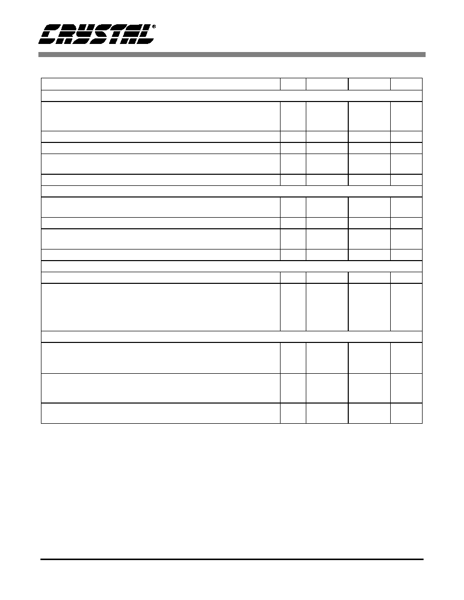
1. CHARACTERISTICS AND SPECIFICATIONS ........................................................................ 4
2. GENERAL DESCRIPTION ..................................................................................................... 10
2.1 Analog Input ..................................................................................................................... 10
2.1.1 Analog Input Model ............................................................................................. 10
2.2 Voltage Reference Input .................................................................................................. 11
2.2.1 Voltage Reference Input Model ........................................................................... 11
2.3 Power Supply Arrangements ........................................................................................... 12
2.4 Clock Generator ............................................................................................................... 12
2.5 Serial Port Interface ......................................................................................................... 12
2.6 Serial Port ........................................................................................................................ 13
2.7 Serial Port Initialization Sequence ................................................................................... 14
2.8 Command Register Quick Reference ............................................................................. 15
2.9 Performing Conversions/Calibrations .............................................................................. 16
2.9.1 Continuous Calibrations and Conversions (reduced output rate) ....................... 16
2.9.2 One Time Calibration followed by Continuous Conversions ............................... 17
2.9.3 Continuous Conversions with Default Calibration Coefficients ........................... 17
2.9.4 Continuous Conversions with Existing Calibration Coefficients .......................... 17
2.9.5 System Calibration .............................................................................................. 17
2.9.6 Reading Conversions .......................................................................................... 17
2.9.7 Output Coding ..................................................................................................... 18
2.9.8 Digital Filter ......................................................................................................... 18
2.10 Sleep and Standby Modes ............................................................................................. 20
2.11 Power-Up Sequence and Initialization ........................................................................... 20
2.12 PCB Layout .................................................................................................................... 20
3. PIN DESCRIPTIONS .............................................................................................................. 22
4. SPECIFICATION DEFINITIONS ............................................................................................. 24
Contacting Cirrus Logic Support
For a complete listing of Direct Sales, Distributor, and Sales Representative contacts, visit the Cirrus Logic web site at:
http://www.cirrus.com/corporate/contacts/
SPI is a trademark of Motorola Inc.
Microwire is a trademark of National Semiconductor Corp.
Preliminary product information describes products which are in production, but for which full characterization data is not yet available. Advance product infor-
mation describes products which are in development and subject to development changes. Cirrus Logic, Inc. has made best efforts to ensure that the informa-
tion contained in this document is accurate and reliable. However, the information is subject to change without notice and is provided "AS IS" without warranty
of any kind (express or implied). No responsibility is assumed by Cirrus Logic, Inc. for the use of this information, nor for infringements of patents or other rights
of third parties. This document is the property of Cirrus Logic, Inc. and implies no license under patents, copyrights, trademarks, or trade secrets. No part of
this publication may be copied, reproduced, stored in a retrieval system, or transmitted, in any form or by any means (electronic, mechanical, photographic, or
otherwise) without the prior written consent of Cirrus Logic, Inc. Items from any Cirrus Logic website or disk may be printed for use by the user. However, no
part of the printout or electronic files may be copied, reproduced, stored in a retrieval system, or transmitted, in any form or by any means (electronic, mechan-
ical, photographic, or otherwise) without the prior written consent of Cirrus Logic, Inc.Furthermore, no part of this publication may be used as a basis for man-
ufacture or sale of any items without the prior written consent of Cirrus Logic, Inc. The names of products of Cirrus Logic, Inc. or other vendors and suppliers
appearing in this document may be trademarks or service marks of their respective owners which may be registered in some jurisdictions. A list of Cirrus Logic,
Inc. trademarks and service marks can be found at http://www.cirrus.com.

CS5541
DS500PP1
3
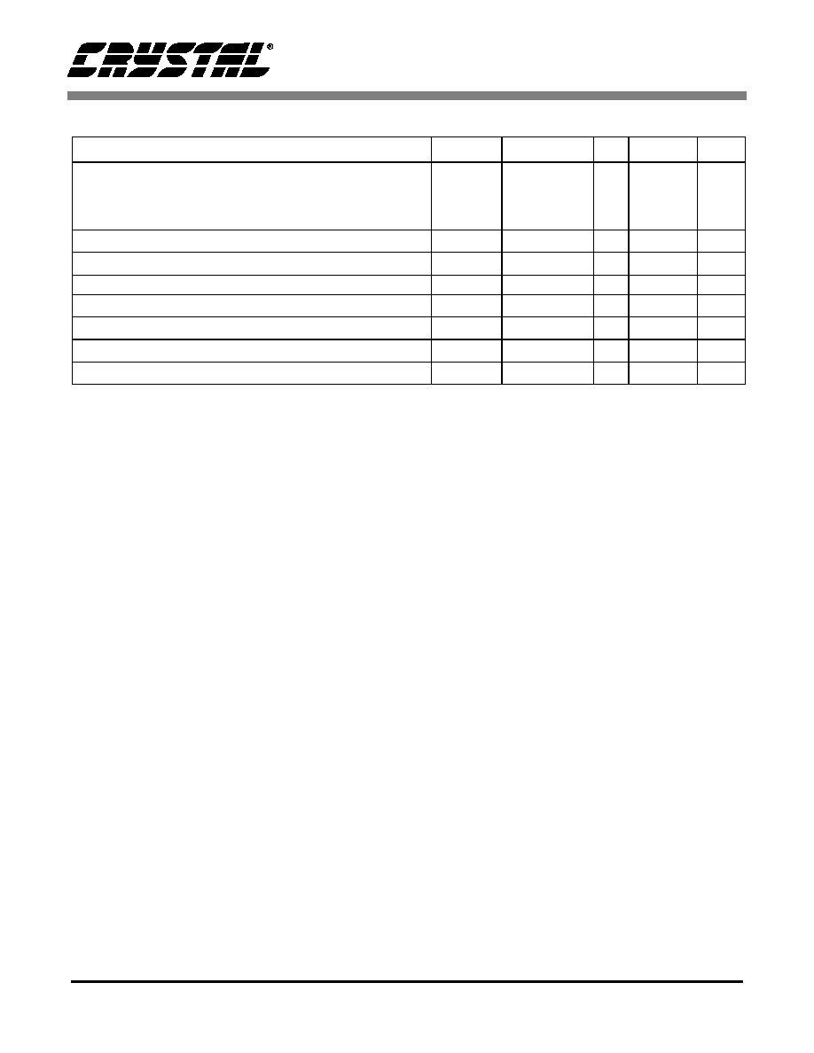
LIST OF FIGURES
Figure 1. Continuous Running SCLK Timing (Not to Scale) ................................ 9
Figure 2. SDI Write Timing (Not to Scale) ............................................................ 9
Figure 3. SDO Read Timing (Not to Scale) .......................................................... 9
Figure 4. Multiplexer Configuration. ................................................................... 10
Figure 5. Input model for AIN+ and AIN- pins. ................................................... 10
Figure 6. Resolution vs. Voltage Reference ....................................................... 11
Figure 7. Resolution vs. Voltage Reference ....................................................... 11
Figure 8. Input model for VREF+ and VREF- pins. ............................................ 11
Figure 9. CS5541 Configured with +3.0 V Analog Supply. ................................ 12
Figure 10. CS5541 Register Diagram. ............................................................... 13
Figure 11. Command and Data Word Timing. ................................................... 13
Figure 12. Self Calibration of Offset. .................................................................. 16
Figure 13. Self Calibration of Gain. .................................................................... 16
Figure 14. Digital Filter 1 Response ................................................................... 19
Figure 15. Filter 2 Response (MCLK = 32.768 kHz) .......................................... 19
LIST OF TABLES
Table 1. Filter Output Word Rates ................................................................................................ 14
Table 2. Output Conversion Data Register Description (24 bits + flags) ...................................... 18
Table 3. CS5541 24-Bit Output Coding......................................................................................... 19

CS5541
4
DS500PP1
1. CHARACTERISTICS AND SPECIFICATIONS
ANALOG CHARACTERISTICS
(T
A
= 25 °C; VA+ = +3 V ±5%, VA- = 0 V, VD+ = +3.0 V ±5%, DGND
= 0 V, VREF+ = 2.5 V, VREF- = 0 V, MCLK = 32.768 kHz, OWR (Output Word Rate) = 53.7 SPS, Bipolar Mode,
Input Range = ±2.5 V Differential, Vcm=1.25 V.) (See Notes 1 and 2.)
Notes: 1. Applies after a one-time self-calibration at any temperature within -40 °C ~ +85 °C.
2. Specifications guaranteed by design, characterization, and/or test.
3. Specification applies to the device only and does not include any effects by external parasitic
thermocouples.
4. Drift over specified temperature range after calibration at power-up at 25
°C.
5. Wideband noise aliased into the baseband. Referred to the input. Typical values shown for 25 °C.
6. For peak-to-peak noise multiply by 6.6 for all ranges and output rates.
7. RMS noise numbers assume continuous calibration mode is not used. In continuous calibration mode
the noise increases by a factor of two.
* Specifications are subject to change without notice.
Parameter
Min
Typ
Max
Units
Accuracy
Linearity Error
-
±0.0015
±0.003
%FS
No Missing Codes
24
-
-
Bits
Bipolar Offset
(Note 3)
-
±16
TBD
LSB
24
Unipolar Offset
(Note 3)
-
±32
TBD
LSB
24
Offset Drift
(Notes 3 and 4)
-
20
-
nV/°C
Bipolar Full Scale Error
-
±8
±31
ppm
Unipolar Full Scale Error
-
±16
±62
ppm
Full Scale Drift
(Note 4)
-
1
-
ppm/°C
Noise
(Notes 5, 6, and 7)
Filter Type
Output Word Rate (SPS) -3 dB Filter Frequency (Hz)
RMS Noise (µV)
Single Conversion Settling with
50/60 Hz Rejection
13.4
11.96
2
Four Conversion Settling with
50/60 Hz Rejection
53.7
11.96
2
Fast Filter with
Single Conversion Settling
64.8
56.91
35
Fast Filter with
Four Conversion Settling
260
56.91
35
CS5541
DS500PP1
5
ANALOG CHARACTERISTICS
(Continued)
Notes: 8. See Section
2.1, "Analog Input
".
9. See Section
2.2, "Voltage Reference Input"
.
10. VREF must be less than or equal to supply voltages.
11. The CS5541 includes two digital filters. The first filter, which achieves simultaneous rejection of 50/60
Hz, provides single conversion settling at 13.4 SPS throughput or four conversion settling at 53.7 SPS
throughput. The second filter, which achieves 16-bit performance, provides single conversion settling at
64.8 SPS throughput or four conversion settling at 260 SPS throughput.
12. All outputs unloaded. All digital inputs at CMOS levels.
Parameter
Min
Typ
Max
Units
Analog Inputs
Common Mode + Signal on AIN+ or AIN-
(Bipolar/Unipolar Mode)
Single Supply
Dual Supply
0.0
VA-
-
-
VA+
VA+
V
V
CVF Current on AIN+, AIN-
(Note 8)
-
12
-
nA
Input Leakage for MUX when off
-
10
-
pA
Common Mode Rejection
dc
50, 60Hz
-
-
120
120
-
-
dB
dB
Input Capacitance
-
8
-
pF
Voltage Reference Inputs
Range
(VREF+) - (VREF-)
(Note 10)
0.1
2.5
(VA+) -
(VA-)
V
CVF Current on VREF+ and VREF-
(Note 9)
-
20
-
nA
Common Mode Rejection
dc
50, 60 Hz
-
-
120
120
-
-
dB
dB
Input Capacitance
-
12
-
pF
Dynamic Characteristics
Modulator Sampling Frequency
-
MCLK/2
-
Hz
Filter Settling to 1/2 LSB (Full Scale Step)
(Note 11)
13.4 SPS OWR
53.7 SPS OWR
64.8 SPS OWR
260 SPS OWR
-
-
-
1/OWR
4/OWR
1/OWR
4/OWR
-
-
-
-
s
s
s
s
Power Supplies
DC Power Supply Currents
(Normal Mode)
I
A+
I
D+
-
-
225
25
280
36
µA
µA
Power Consumption
Normal Mode
(Note 12)
Standby Mode
Sleep Mode
-
-
-
750
75
30
1000
-
-
µW
µW
µW
Power Supply Rejection
dc Positive Supplies
dc Negative Supply
-
-
80
80
-
-
dB
dB

CS5541
6
DS500PP1
3 V DIGITAL CHARACTERISTICS
(T
A
= 25 °C; VA
+ = 3.0 V ±5%, VA- = 0 V, VD+ = 3.0 V ± 5%,
DGND = 0 V.)(See Notes 2 and 13.)
Notes: 13. All measurements performed under static conditions.
Parameter
Symbol
Min
Typ
Max
Units
High-Level Input Voltage:
All Pins Except
OSC1, SCLK
OSC1
SCLK
V
IH
V
IH
V
IH
0.6VD+
TBD
(VD+)-0.45
-
-
-
-
-
-
V
V
V
Low-Level Input Voltage:
All Pins Except
OSC1, SCLK
OSC1
SCLK
V
IL
V
IL
V
IL
-
-
-
-
-
-
0.16VD+
TBD
0.6
V
V
V
High-Level Output Voltage:
(SDO pin)
I
out
= -1.0 mA
V
OH
(VD+)-0.25
-
-
V
Low-Level Output Voltage:
(SDO pin)
I
out
= 1.0 mA
V
OL
-
-
0.2
V
Input Leakage Current
I
in
-
±1
±10
µA
3-State Leakage Current
I
OZ
-
-
±10
µA
Digital Output Pin Capacitance
C
out
-
9
-
pF
CS5541
DS500PP1
7
ABSOLUTE MAXIMUM RATINGS
(DGND = 0 V) (See Note 14.)
Notes: 14. All voltages measured with respect to digital ground (DGND).
15. VA+ and VA- must satisfy {(VA+) - (VA-)}
+4.0 V.
16. VD+ and VA- must satisfy {(VD+) - (VA-)}
+4.0 V.
17. Applies to all pins including continuous overvoltage conditions at the analog input (AIN) pins.
18. Transient currents up to 100 mA will not cause SCR latch-up. Maximum input current for a power
supply pin is ±50 mA.
19. Total power dissipation, including all input currents and output currents.
WARNING: Operation at or beyond these limits may result in permanent damage to the device.
Normal operation is not guaranteed at these extremes.
Parameter
Symbol
Min
Typ
Max
Units
DC Power Supplies
(Notes 15 and 16)
Positive Digital
Positive Analog
Negative Analog
VD+
VA+
VA-
-0.3
-0.3
-0.3
-
-
-
+4.0
+4.0
+0.3
V
V
V
Input Current, Any Pin Except Supplies
(Notes 17 and 18)
I
IN
-
-
±10
mA
Output Current
I
OUT
-
-
±25
mA
Power Dissipation
(Note 19)
PDN
-
-
500
mW
Analog Input Voltage
AIN and VREF pins
V
INA
(VA-) + (-0.3)
-
(VA+)+0.3
V
Digital Input Voltage
V
IND
-0.3
-
(VD+)+0.3
V
Ambient Operating Temperature
T
A
-40
-
+85
°C
Storage Temperature
T
stg
-65
-
+150
°C

CS5541
8
DS500PP1
SWITCHING CHARACTERISTICS
(T
A
= 25 °C; VA+ = +3.0 V ±5% VA- = 0 V, VD+ = 3.0 V ±5%,
DGND = 0 V; Input Levels: Logic 0 = 0 V, Logic 1 = VD+; C
L
= 50 pF)
Notes: 20. Device parameters are specified with 32.768 kHz clock; however, clocks up to 40 kHz can be used for
increased throughput.
21. Specified using 10% and 90% points on waveform of interest. Output loaded with 50 pF.
22. Oscillator start-up time varies with crystal parameters. This specification does not apply when using an
external clock source.
Parameter
Symbol
Min
Typ
Max
Units
Master Clock Frequency:
External Clock
Internal Oscillator (Note 20)
MCLK
5
-
-
32.768
40
-
kHz
Master Clock Duty Cycle
40
-
60
%
Rise Times
(Note 21)
Any Digital Input Except SCLK
SCLK
Any Digital Output
t
rise
-
-
-
-
-
50
1.0
100
-
µs
µs
ns
Fall Times
(Note 21)
Any Digital Input Except SCLK
SCLK
Any Digital Output
t
rise
-
-
-
-
-
50
1.0
100
-
µs
µs
ns
Start-up
Oscillator Start-up Time
XTAL = 32.768 kHz (Note 22)
t
ost
-
500
-
ms
Power-on-Reset Period
t
por
-
490
-
MCLK
cycles
Serial Port Timing
Serial Clock Frequency
SCLK
0
-
2
MHz
Serial Clock
Pulse Width High
Pulse Width Low
t
1
t
2
250
250
-
-
-
-
ns
ns
SDI Write Timing
CS Enable to SCLK Rising
t
3
50
-
-
ns
Data Set-up Time prior to SCLK rising
t
4
50
-
-
ns
Data Hold Time After SCLK Rising
t
5
100
-
-
ns
SCLK Falling Prior to CS Disable
t
6
100
-
-
ns
SDO Read Timing
CS to Data Valid
t
7
-
-
150
ns
SCLK Falling to New Data Bit
t
8
-
-
150
ns
CS Rising to SDO Hi-Z
t
9
-
-
150
ns

CS5541
DS500PP1
9
Figure 1. Continuous Running SCLK Timing (Not to Scale)
CS
SCLK
t1
t6
t2
t3
Figure 2. SDI Write Timing (Not to Scale)
CS
SCLK
MSB
MSB-1
LSB
SDI
t3
t6
t4
t5
t1
t2
Figure 3. SDO Read Timing (Not to Scale)
CS
SCLK
MSB
MSB-1
LSB
SDO
t7
t9
t8
t1
t2
CS5541
10
DS500PP1
2. GENERAL DESCRIPTION
The CS5541 is a 24-bit, low-power and low-volt-
age
- analog-to-digital converter (ADC). It is
optimized to convert analog signals in DC mea-
surement applications such as temperature
and
pressure
measurement, and various portable devic-
es where low power consumption is required.
To accommodate these applications, the ADC inte-
grates analog input and reference buffers for in-
creased input impedance and includes a
two-channel multiplexer. Absolute accuracy is
achieved via one-time or continuous calibration
modes. The device also operates with a variety of
supply configurations while drawing less than 330
µA.
The CS5541 includes two digital filters. The first
filter which achieves simultaneous rejection of
50/60 Hz provides single conversion settling at
13.4 SPS throughput or four conversion settling at
53.7 SPS throughput. The second filter which
achieves 16-bit performance provides single con-
version settling at 64.8 SPS throughput or four con-
version settling at 260 SPS throughput. (Either
filter's output word rates can be increased by using
a faster master clock, up to 40 kHz).
To ease communication between the ADCs and a
microcontroller, the converters include a simple
three-wire serial interface which is SPI and Mi-
crowire compatible. A Schmitt Trigger input is pro-
vided on the serial clock (SCLK) input.
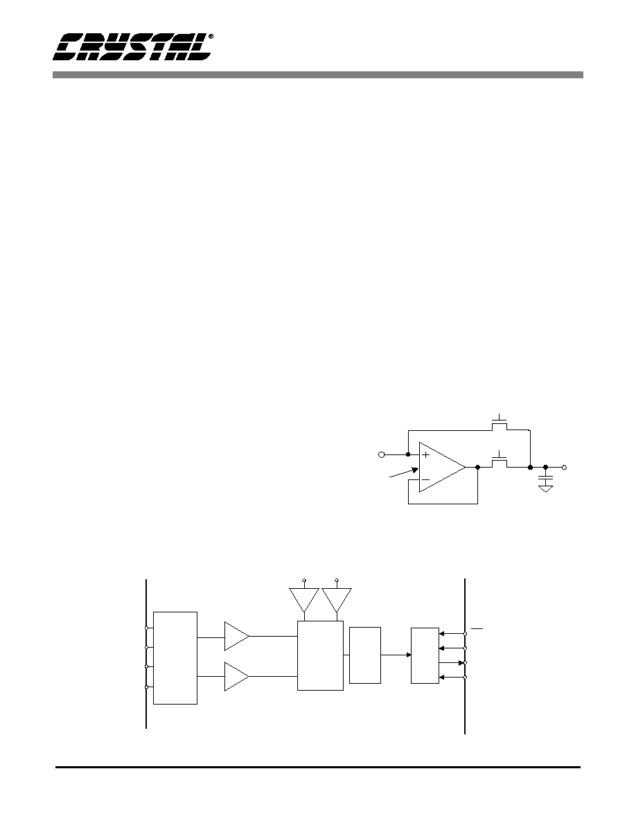
2.1 Analog Input
Figure 4 illustrates a block diagram of the CS5541.
The device consists of a multiplexer, a unity gain
coarse/fine charge input buffer, a fourth order
-
modulator, and a digital filter.
2.1.1 Analog Input Model
Figure 5 illustrates the input models for the AIN
pins. The model includes a coarse/fine charge buff-
er which reduces the dynamic current demand on
the analog input signal. The buffer is designed to
accommodate rail to rail (common-mode plus sig-
nal) input voltages. Typical CVF (sampling) cur-
rent is about 12 nA (MCLK = 32.768 kHz).
Application Note 30, "Switched-Capacitor A/D In-
put Structures", details various input architectures.
VREF+
Sinc
Digital
Filter
M
U
X
AIN2+
AIN2-
AIN1+
AIN1-
X1
X1
X1
VREF-
X1
Differential
4 Order
Modulator
th
4
Serial
Port
CS
SDI
SDO
SCLK
Figure 4. Multiplexer Configuration.
AIN
C = 8 pF
f = 2*MCLK = 65.536 kHz
Coarse
2
Fine
1
i
n
= CV
os
f
V
os
25mV
Figure 5. Input model for AIN+ and AIN- pins.

CS5541
DS500PP1
11
2.2 Voltage Reference Input
The differential voltage between VREF+ and
VREF- sets the nominal full scale input range of
the converter. For a single-ended reference voltage,
the reference output is connected to the VREF+ pin
of the CS5541 and the ground reference is connect-
ed to the VREF- pin. Note that the differential ref-
erence voltage can be from 0.1 V to ((VA+)-
(VA-)). The noise-free resolution of a single sam-
ple from the ADC is directly proportional to the
voltage reference as depicted in Figures 6 and 7.
Note:
When a lower reference voltage is used, the
resulting code widths are smaller. Since the
output codes exhibit more changing codes for
a fixed amount of noise, the converter
appears noisier.
2.2.1 Voltage Reference Input Model
Figure 8 illustrates the input models for the VREF
pins. It includes a coarse/fine charge buffer which
reduces the dynamic current demand on the exter-
nal reference. The reference's buffer is designed to
accommodate rail-to-rail (common-mode plus sig-
nal) input voltages. Typical CVF (sampling) cur-
rent is about 20 nA (MCLK = 32.768 kHz; see
Figure 8).
14
15
16
17
18
19
20
0
0.5
1
1.5
2
2.5
3
VREF (V)
Noi
se-
Free Resol
u
t
i
on (
B
i
t
s)
Figure 6. Typical Noise-Free Resolution
vs. Voltage Reference
One-Time Cal, 4 Cycle Settling, 50/60 Hz Reject
Noise-Free Res. = log
2
(Bipolar Span/6.6*RMS Noise)
13
14
15
16
17
18
19
0
0.5
1
1.5
2
2.5
3
VREF (V)
N
o
i
se-Free R
esol
u
ti
on (B
i
t
s)
Figure 7. Typical Noise-Free Resolution
vs. Voltage Reference
Continuous Cal, 1Cycle Settling, 50/60 Hz Reject
Noise-Free Res. = log
2
(Bipolar Span/6.6*RMS Noise)
VREF
C = 12 pF
f = 2*MCLK = 65.536 kHz
Coarse
2
Fine
1
i
n
= CV
os
f
V
os
25mV
Figure 8. Input model for VREF+ and VREF- pins.
CS5541
12
DS500PP1
2.3 Power Supply Arrangements
The CS5541 is designed to operate with a total sup-
ply voltage of 3.0 V ± 5%. For maximum flexibility
separate pins are provided for VA+, VA-, VD+,
and DGND, which is especially useful with ground
referenced input signals.
Figure 9 illustrates the CS5541 connected with a
single +3.0 V supply for both the analog and digital
sections.
2.4 Clock Generator
The CS5541 includes an oscillator circuit which
can be connected with an external crystal to pro-
vide the master clock for the chip. The chip is de-
signed to operate using a low-cost 32.768 kHz
"tuning fork" type crystal. One lead of the crystal
should be connected to OSC1 and the other to
OSC2. A 10 Megohm resistor should be connected
in parallel with the crystal. Lead lengths should be
minimized to reduce stray capacitance. The con-
verter will operate with an external (CMOS com-
patible) clock applied at OSC1 with frequencies up
to 40 kHz.
2.5 Serial Port Interface
The CS5541's serial interface consists of four con-
trol lines: CS, SDI, SDO, and SCLK.
CS, Chip Select, is the control line which enables
access to the serial port. If the CS pin is tied to logic
0, the port will function as a three wire interface.
SDI, Serial Data In, is the data signal used to trans-
fer data to the converters.
SDO, Serial Data Out, is the data signal used to
transfer output data from the converters. The SDO
output will be held at high impedance any time CS
is at logic 1.
SCLK, Serial Clock, is the serial bit-clock which
controls the shifting of data to or from the ADC's
serial port. The CS pin must be held at logic 0 be-
fore SCLK transitions can be recognized by the
port logic. To accommodate opto-isolators SCLK
is designed with a Schmitt-trigger input.
OSC2
VD+
VA+
VREF+
VREF-
DGND
AIN1+
SCLK
SDO
SDI
CS5541
OSC1
CS
+3.0 V
Analog
16
15
3
1
11
9
8
7
6
10
5
12
Optional Clock
Source
Serial
Data
Interface
5 kHz ~ 40 kHz
AIN1-
4
VA-
2
0.1
µF
0.1
µF
10
AIN2+
AIN2-
+
-
Voltage
Reference
14
13
Analog
Signal
Sources
Supply
10 M
Figure 9. CS5541 Configured with +3.0 V Analog Supply.
CS5541
DS500PP1
13
2.6 Serial Port
The CS5541 includes a state machine with an 8-bit
command register, which instructs the ADC to per-
form conversions, and a 24-bit conversion data reg-
ister (read only) to store conversion results. Figure
10 illustrates a block diagram of the internal regis-
ters.
After power is applied to the ADC (the ADC in-
cludes a power-on reset circuit) or after the user
transmits the serial port initialization sequence, the
serial port is set to the command mode. The con-
verter stays in this mode until a valid 8-bit com-
mand is received (the first 8 bits into the serial
port). Once a valid 8-bit data mode command is re-
ceived and interpreted by the ADC's command
register, the serial port enters the data mode and
continuous conversions are performed. The SDO
pin falls at the end of a conversion and the user may
read the conversion data by providing 32 serial
clocks (SCLKs), as shown in Figure 11 . The first 8
SCLKs are needed to clear the SDO flag and to
read the status flags. During the next 24 SCLKs,
the conversion data is shifted out of the serial port.
To continue performing the conversions, SDI must
be kept low during the status read time. A new
command can be issued any time other than during
the data read. If the command happens to be a pow-
er save command, the serial port goes back to the
command mode. Otherwise, the conversions will
stop in progress and start new conversions based on
the information in the command byte, and the serial
port will remain in the data mode. Section 2.8,
"Command Register Quick Reference", lists all
valid commands.
2.7 Serial Port Initialization Sequence
To initialize the serial port of the ADC to the com-
mand mode, the user can transmit the serial port
initialization sequence. The port initialization se-
quence involves clocking seven (or more) SYNC1
command bytes (0xFF) followed by one SYNC0
command byte (0xFE). Note that this sequence
places the ADC's serial port in the command mode
where it waits until a valid command is received.
This sequence does not reset the internal registers
to their default settings. Further note that the se-
quence can be issued at any time and aids signifi-
cantly in initial code development.
Serial
Interface
CS
SDI
SDO
SCLK
Command Register (1 × 8)
W
r
it
e O
n
ly
Read O
n
ly
Conversion Data Register (1x24)
Figure 10. CS5541 Register Diagram.
1st Command Time
8 SCLKs
SDO
SCLK
SDI
t
d
*
Data Time
24 SCLKs
MSB
LSB
0
1
CH OD OF
1
1
8 SCLKs to read status
SDI set low while
reading status & data
1
t
o
*
* t
d
, t
o
- Refer to Table 1. for output timing.
Figure 11. Command and Data Word Timing.

CS5541
14
DS500PP1
2.8 Command Register Quick Reference
Notes: 23. After entering a Power Save Mode, the user must wait a minimum of 2 system clocks before issuing a
convert command.
24. A Power Save Mode cannot be entered by selectively setting the D5 bit.
0xAX must be written to the command register before the Sleep Mode will be enabled.
Similarly, 0xBX must be written to the command register before the Standby Mode will be enabled.
25. If Four Cycle Settling is selected (D3 = '1'), the part will perform a one-time calibration when continuous
calibration is chosen.
D7(MSB)
D6
D5
D4
D3
D2
D1
D0
CB
CH
PS
U/B
FS1
FS0
C1
C0
BIT
NAME
VALUE
FUNCTION
D7
Command Bit, CB
0
1
Reserved
Logic 1 for executable commands
D6
Channel Select, CH
0
1
Activate AIN1 for conversion
Activate AIN2 for conversion
D5
Power Save, PS
Notes 23, 24
0
1
Data Mode
Power Save Mode (Standby or Sleep)
D4
Unipolar/Bipolar, U/B
0
1
Bipolar Conversion Mode
Unipolar Conversion Mode
D3-D2
Filter Select, FS1-FS0
Note 25
00
01
10
11
Single Cycle Settling, 50/60 Hz Reject
Single Cycle Settling, No 50/60 Hz Reject
Four Cycle Settling, 50/60 Hz Reject
Four Cycle Settling, No 50/60 Hz Reject
D1-D0
Conversion Calibration
Select, C1-C0
00
01
10
11
Calibrate prior to each point
Perform a one time calibration
Use default calibration coefficients for conversions
Use existing calibration coefficients for conversion

CS5541
DS500PP1
15
2.9 Performing Conversions/Calibrations
The CS5541 offers four conversion/self-calibration
modes (if a user requires system calibration, this
can be accommodated in the system microcontrol-
ler). The first mode allows the user to calibrate con-
tinuously between each conversion. The second
mode allows the user to calibrate once after the
command is issued and then continuously convert
on the channel selected using the calibration result.
The third mode allows the user to skip calibration;
however, it performs conversions with the default
calibration coefficients. The final mode allows the
user to use the previous calibration coefficients to
perform continuous conversions on the channel se-
lected. The sections that follow detail the differenc-
es between the conversion modes. The sections
also explain how to decode the conversion word
into the respective flag and data bits.
2.9.1 Continuous Calibrations and Conver-
sions (reduced output rate)
This mode performs an offset and gain calibration
prior to each conversion. Note that the effective
throughput in this mode is reduced by two as a cal-
ibration is performed prior to each conversion.
Nevertheless, after the first command instructing
the ADC to enter this mode is given, an offset cali-
bration is performed followed by a gain calibration.
Then the first data conversion is performed. Subse-
quent conversions are offset calibration followed
by data conversion. Then, a gain calibration is per-
formed followed by a data conversion. The ADC
repetitively steps through this sequence until a new
command is issued.
Note:
The CS5541 offers self calibration where the
ADC calibrates out offset and gain errors due
to the ADC itself. Calibration in the CS5541 is
used to set the zero and gain slope of the
ADC's transfer function. For the
self-calibration of offset, the converter
internally ties the inputs of the modulator
together and routes them to the VREF- pin as
shown in Figure 12. VREF- must be tied to a
fixed voltage between VA+ and VA-. For
self-calibration of gain, the differential inputs
of the modulator are connected to VREF+
and VREF- as shown in Figure 13. Further
note that each calibration step (offset or gain)
takes one conversion cycle to complete.
However, after the ADC is reset, it is
functional and can perform measurements
without being calibrated (see Perform
Continuous Conversions with Default
Calibration Coefficients section for details). In
this case, the converter will utilize the
initialized values of the on-chip registers
(Offset = 0, Gain = 1.0) to calculate output
words. Any initial offset and gain errors in the
internal circuitry of the chip will remain.
AIN+
AIN-
+
-
VREF-
Figure 12. Self Calibration of Offset.
AIN+
AIN-
+
-
VREF+
VREF-
+
-
Reference
Figure 13. Self Calibration of Gain.

CS5541
16
DS500PP1
2.9.2 One Time Calibration followed by Con-
tinuous Conversions
After the first command instructing the ADC to en-
ter this mode is given, an offset calibration is per-
formed followed by a gain calibration. Then the
first data conversion is performed. Subsequent con-
versions do not include new calibrations. This al-
lows the ADC to provide maximum throughput for
the filter rate selected.
2.9.3 Continuous Conversions with Default
Calibration Coefficients
After the command instructing the ADC to enter
this mode is given, the ADC will utilize the initial-
ized values of the on-chip calibration registers
(Offset = 0, Gain = 1.0) for all conversions. This al-
lows the ADC to provide maximum throughput for
the filter rate selected. This mode is recommended
when the user is performing a system calibration.
2.9.4 Continuous Conversions with Existing
Calibration Coefficients
After the command instructing the ADC to enter
this mode is given, the ADC will use the coeffi-
cients from the previous calibration to calculate
conversions. If no prior calibration has been per-
formed since power-up, the ADC will use the de-
fault calibration coefficients (Offset = 0, Gain = 1).
The ADC performs conversions at the maximum
throughput for the filter rate selected.
2.9.5 Output Word Timing
Table 1 describes the output word timing of the
CS5541. D3-D0 are the last four bits of the com-
mand word issued, as described in Section 2.8.
Both t
d
and t
o
are represented graphically in Figure
11. t
d
represents the amount of time for a conver-
sion to be completed, once a valid command is re-
ceived. t
o
is the time required for all subsequent
conversions, before a new command is received.
"Throughput" is the rate at which those subsequent
conversions are output.
Notes: 26. t
d
can be off by one MCLK cycle if SCLK is asynchronous to MCLK.
27. Throughput calculations assume that MCLK = 32.768 kHz.
D3-D0
t
d
-
First Output (cycles)
Note 26
t
o
-
Subsequent Outputs (cycles)
Throughput (SPS)
Note 27
0000
7358
4884
6.7093
0001
7358
2442
13.418
001x
2474
2442
13.418
0100
1550
1012
32.379
0101
1550
506
64.759
011x
538
506
64.759
100x
7358
610
53.718
101x
2474
610
53.718
110x
1550
126
260.06
111x
538
126
260.06
Table 1. Filter Output Word Rates

CS5541
DS500PP1
17
2.9.6 System Calibration
If a system level calibration is to be performed us-
ing a system microcontroller, it is best to put the
converter in the Continuous Conversions with De-
fault Calibration Coefficients mode. The user
would configure the system with a zero-level input
and store the resulting conversion for system offset
correction. Then the user would configure the sys-
tem with a full-scale input level and store the re-
sulting conversion for system full-scale correction.
Correction of converter data is then performed us-
ing the system microcontroller.
2.9.7 Reading Conversions
At the completion of a conversion, SDO will fall to
logic 0 to indicate that the conversion is complete.
If calibration modes are used they will be transpar-
ent to user and only affect the effective throughput
of the ADC. Nevertheless, to read a conversion
word, the user must issue 8 SCLKs (SDI = logic 0
for the NULL command and remain in this mode or
SDI can be used to clock in a new command) to
clear the SDO flag and read the status flags. Upon
the falling edge of the 8
th
SCLK, the SDO pin will
present the first bit (MSB) of the conversion word.
24 SCLKs (high, then low) are then required to
read the conversion word from the port. Upon the
falling edge of the 32
nd
SCLK, SDO will return
high, waiting till the next conversion is complete
before it falls again.
When operating in any of the conversion modes,
the user need not read every conversion. If the user
chooses not to read a conversion after SDO falls,
SDO will rise one MCLK clock cycle before the
next conversion is completed and then fall to signal
that another conversion word is available. To exit
the particular conversion mode, the user must issue
any valid command, other than the NULL com-
mand, to the SDI input. The new command can be
issued anytime other than during the data read. If
the user wants to read the last conversion data and
issue the new command, the following protocol is
required: After SDO falls, read the status flags
(keeping SDI low, 8 SCLKs), followed by the con-
version data (24 SCLKs). Then follow it up with
the new command at SDI (8 SCLKs).
If the command happens to be a power save com-
mand, the serial port goes back to the command
mode. Otherwise, the conversion will stop in
progress and start new conversions based on the in-
formation in the command byte, and the serial port
remains in the data mode.
Note:
1) If the user begins to clear the SDO end-of-
conversion flag and read the conversion data,
this action must be finished before the
conversion cycle which is occurring in the
background is complete if the user wants to
be able to read the new conversion data.
2) If a new conversion command is issued to
the converter while it is performing a
conversion, the filter will stop the current
conversion and start a new convolution cycle
to perform a new conversion.
3) If a new conversion command is issued
when SDO is low, SDO will output 01111,
then CH, OD, and OF. Afterwards, SDO will
remain high until one MCLK cycle before the
new data is ready, then fall to indicate that the
conversion is completed.
2.9.8 Output Coding
The CS5541 outputs 24-bit data conversion words.
To read a conversion word the user must read the
conversion data register. The conversion data reg-
ister is 24 bits long and outputs the data word MSB
first. Once a conversion is complete, SDO falls and
32 SCLK's are required to read the results. The first
8 SCLKs are used to clear the SDO flag and clock
out the status flags.
The Channel Indicator (CH) bit keeps track of
which input channel was converted.
The Oscillation Detect (OD) bit is set to a logic 1 any
time that an oscillatory condition is detected in the
modulator. This does not occur under normal oper-
ating conditions, but may occur whenever the input
to the converter is extremely overranged. If the OD
bit is set, the conversion data bits can be completely

CS5541
18
DS500PP1
erroneous. The OD flag bit will be cleared to logic 0
when the modulator becomes stable.
The Overrange Flag (OF) bit is set to a logic 1 any
time the input signal is: 1) more positive than posi-
tive full scale, 2) more negative than zero (unipolar
mode), 3) more negative than negative full scale
(bipolar mode). It is cleared back to logic 0 when-
ever a conversion word occurs which is not over-
ranged.
The last 24 SCLKs are used to clock data out of the
conversion data register.
Table 2 and Table 3 illustrate the output coding for
the CS5541. Unipolar conversions are output in bi-
nary format and bipolar conversions are output in
two's complement format.
2.9.9 Digital Filter
The CS5541 includes two digital filters. The first
filter which achieves simultaneous rejection of
50/60 Hz provides single conversion settling at
13.4 SPS throughput or four conversion settling at
53.7 SPS throughput. The second filter which
achieves 16-bit performance provides single con-
version settling at 64.8 SPS throughput or four con-
version settling at 260 SPS throughput.
The first filter (13.4 SPS and 53.7 SPS throughput)
is optimized to yield better than 80 dB rejection be-
tween 47 Hz to 63 Hz (i.e. 80 dB minimum rejec-
tion for both 50 Hz and 60 Hz) when the master
clock is 32.768 kHz. The filter has a response as
shown in Figure 14.
The second filter is optimized for higher through-
put, and does not provide 50 Hz or 60 Hz rejection.
It has a frequency response that is shown in Figure
15.
To ease code development, each filter (13.4 SPS or
64.8 SPS throughput) has a mode that only outputs
fully settled output conversions (every 4
th
convolu-
tion).
D31
D30
D29
D28
D27
D26
D25
D24
0
1
1
1
1
CH
OD
OF
D23
D22
D21
D20
D19
D18
D17
D16
D15
D14
D13
D12
MSB
22
21
20
19
18
17
16
15
14
13
12
D11
D10
D9
D8
D7
D6
D5
D4
D3
D2
D1
D0
11
10
9
8
7
6
5
4
3
2
1
LSB
Table 2. Output Conversion Data Register Description (24 bits + flags)
Note:
VFS in the table equals the voltage between ground and full scale for the unipolar mode, or the voltage
between
± full scale for the bipolar mode. See text about error flags under overrange conditions.
Unipolar Input Voltage
Offset Binary
Bipolar Input Voltage
Two's
Complement
>(VFS-1.5 LSB)
FFFFFF
>(VFS-1.5 LSB)
7FFFFF
VFS-1.5 LSB
FFFFFF
-----
FFFFFE
VFS-1.5 LSB
7FFFFF
-----
7FFFFE
VFS/2-0.5 LSB
800000
-----
7FFFFF
-0.5 LSB
000000
-----
FFFFFF
+0.5 LSB
000001
-----
000000
-VFS+0.5 LSB
800001
-----
800000
<(+0.5 LSB)
000000
<(-VFS+0.5 LSB)
800000
Table 3. CS5541 24-Bit Output Coding

CS5541
DS500PP1
19
To accommodate higher throughput requirements,
each filter has a mode (53.7 SPS or 260 SPS
throughput) that outputs every single convolution.
This allows users to see input signal trends at high-
er update rates.
Note:
The converter's digital filter characteristics
linearly scale with MCLK.
2.10 Sleep and Standby Modes
The CS5541 accommodates three power consump-
tion modes: normal, sleep, and standby. The nor-
mal power consumption mode is entered by default
after a power-on-reset. In this mode, the CS5541
typically consumes 750 µW.
The Sleep Mode is entered whenever the sleep
command, 0xAX, is issued to the serial port. The
ADC immediately enters sleep after the command
is issued, reducing the consumed power to around
30 µW. During sleep, most of the analog portion of
the chip is powered down and filter convolutions
are halted. To exit sleep (i.e. to return to normal
power consumption mode), the user must transmit
a data mode command. Since the sleep mode dis-
ables the oscillator, approximately a 500 ms crystal
oscillator start-up delay period is required before
the ADC returns to the normal power consumption
mode. Note that if an external clock is used, the
ADC will return to normal power mode within 3
milliseconds.
The Standby Mode is entered by writing 0xBX to
the part. The Standby Mode performs the same
function as the Sleep Mode except that the oscilla-
tor is not powered down. This eliminates the crystal
oscillator start-up time, with a return to normal
power within 3 milliseconds. Again, to exit standby
(i.e. to return to normal power consumption mode),
the user must transmit a data mode command. The
power during Standby will be around 75 µW.
2.11 Power-Up Sequence and Initialization
Care must be taken to assure that no pins are ever
taken below the negative analog supply (VA-) po-
tential. The analog and digital supplies should be
applied simultaneously to assure that the power-on
reset circuit will automatically reset the ADC when
both supplies are at acceptable levels.
Commands should not be sent to the ADC until a
stable clock is present. If a 32.768 kHz crystal is
being used, it will take approximately 500 ms for
the oscillator to stabilize after power has been ap-
plied to the converter. If a CMOS compatible
source with no start-up delay is used, then the ADC
is immediately ready for a command.
After a valid reset, the ADC is placed into the com-
mand state where it waits for a valid command to
execute. Once a valid conversion command has
been received, conversions will begin and data can
be read using the serial port.
Note:
The CS5541 includes an on-chip power-on
reset circuit to automatically reset the ADC
shortly after power-up. When power to the
CS5541 is applied, the ADC is held in a reset
condition until the master clock has started
and a counter-timer elapses (i.e. the
counter-timer counts 490 MCLK cycles to
-140
-120
-100
-80
-60
-40
-20
0
0
20
40
60
80
100
120
Frequency (Hz)
Ma
gni
tude
(
d
B
)
47 Hz
63 Hz
Figure 14. Filter 1 Response (MCLK = 32.768 kHz)
-140
-120
-100
-80
-60
-40
-20
0
0
100
200
300
400
500
Frequency (Hz)
M
a
gnitude (dB)
Figure 15. Filter 2 Response (MCLK = 32.768 kHz)

CS5541
20
DS500PP1
make sure the oscillator is fully stable). In
normal start-up conditions, this power on
reset circuit should reset the chip when power
is applied. If your application could
experience abnormal power start-up
conditions, it is recommended that the serial
port reinitialization sequence, followed by a
power save command, be performed to
guarantee that the converter begins proper
operation.
2.12 PCB Layout
The CS5541 should be placed entirely over an ana-
log ground plane with the DGND pin of the device
connected to the analog ground plane. Place the an-
alog-digital plane split immediately adjacent to the
digital portion of the chip
See the CDB5540/41 data sheet for suggested lay-
out details and Applications Note 18 for more de-
tailed layout guidelines.
Applications Engineering provides a free and con-
fidential Schematic Review Service.
CS5541
DS500PP1
21
3. PIN DESCRIPTIONS
Clock Generator
OSC1; OSC2 - Master Clock.
An inverting amplifier inside the chip is connected between these pins and can be used with a
crystal to provide the master clock for the device. Alternatively, an external (CMOS
compatible) clock (powered relative to VD+) can be supplied into the OSC1 pin to provide the
master clock for the device.
Control Pins and Serial Data I/O
CS - Chip Select.
When active low, the port will recognize SCLK. When high the SDO pin will output a high
impedance state. CS should be changed when SCLK = 0.
SDI - Serial Data Input.
SDI is the input pin of the serial input port. Data will be input at a rate determined by SCLK.
SDO - Serial Data Output.
SDO is the serial data output. It will output a high impedance state if CS = 1.
SCLK - Serial Clock Input.
A clock signal on this pin determines the input/output rate of the data for the SDI/SDO pins
respectively. This input is a Schmitt trigger to allow for slow rise time signals. The SCLK pin
will recognize clocks only when CS is low.
1
2
3
4
5
6
7
8
9
10
11
12
13
14
15
16
VREF+
VREF-
AIN2+
AIN2-
DGND
VD+
SDO
SCLK
CS
AIN1-
AIN1+
VA+
VA-
OSC2
OSC1
SDI
C
S
5541

CS5541
22
DS500PP1
Measurement and Reference Inputs
AIN1+, AIN1-, AIN2+, AIN2- - Differential Analog Input.
Differential input pins into the device.
VREF+, VREF- - Voltage Reference Input.
Fully differential inputs which establish the voltage reference for the on-chip modulator.
Power Supply Connections
VA+ - Positive Analog Power.
Positive analog supply voltage.
VA- - Negative Analog Power.
Negative analog supply voltage.
VD+ - Positive Digital Power.
Positive digital supply voltage.
DGND - Digital Ground.
Digital Ground.

CS5541
DS500PP1
23
4. SPECIFICATION DEFINITIONS
Linearity Error
The deviation of a code from a straight line which connects the two end points of the A/D
Converter transfer function. One end point is located 1/2 LSB below the first code transition
and the other end point is located 1/2 LSB beyond the code transition to all ones. Units in
percent of full-scale.
Differential Nonlinearity
The deviation of a code's width from the ideal width. Units in LSBs.
Full Scale Error
The deviation of the last code transition from the ideal [{(VREF+) - (VREF-)} - 3/2 LSB].
Units are in LSBs.
Unipolar Offset
The deviation of the first code transition from the ideal (1/2 LSB above the voltage on the
AIN- pin). When in unipolar mode (U/B bit = 1). Units are in LSBs.
Bipolar Offset
The deviation of the mid-scale transition (111...111 to 000...000) from the ideal (1/2 LSB below
the voltage on the AIN- pin). When in bipolar mode (U/B bit = 0). Units are in LSBs.

CS5541
24
DS500PP1
Notes: 1. "D" and "E1" are reference datums and do not included mold flash or protrusions, but do include mold
mismatch and are measured at the parting line, mold flash or protrusions shall not exceed 0.20 mm per
side.
2. Dimension "b" does not include dambar protrusion/intrusion. Allowable dambar protrusion shall be
0.13 mm total in excess of "b" dimension at maximum material condition. Dambar intrusion shall not
reduce dimension "b" by more than 0.07 mm at least material condition.
3. These dimensions apply to the flat section of the lead between 0.10 and 0.25 mm from lead tips.
INCHES
MILLIMETERS
NOTE
DIM
MIN
NOM
MAX
MIN
NOM
MAX
A
--
--
0.084
--
--
2.13
A1
0.002
0.005
0.010
0.05
0.13
0.25
A2
0.064
0.069
0.074
1.68
1.75
1.88
b
0.009
0.012
0.015
0.22
--
0.38
2,3
D
0.232
0.244
0.256
5.90
6.20
6.50
1
E
0.291
0.307
0.323
7.40
7.80
8.20
E1
0.197
0.209
0.220
5.00
5.30
5.60
1
e
0.022
0.026
0.030
0.55
0.65
0.75
L
0.025
0.0295
0.041
0.63
0.75
1.03
0°
4°
8°
0°
4°
8°
JEDEC #: MO-150
16L SSOP PACKAGE DRAWING
E
N
1 2 3
e
b
2
A1
A2
A
D
SEATING
PLANE
E1
1
L
SIDE VIEW
END VIEW
TOP VIEW

· Notes ·
