Document Outline
- Features
- Description
- 1. characteristics/specifications
- 2. general description
- 3. System Design
- 3.1 Power Supply Voltages
- VDD1, GND1 - Pins 54, 53
- VDD2, GND2 - Pins 11, 25, 24, 38
- VD, GND - Pins 7, 40, 6, 23, 39
- 3.2 Clock and Synchronization Signals
- 3.3 EEPROM Programming
- 3.4 Boundary Scan Testing
- 3.5 Functional Testing
- 3.6 System Registers
- 4. Reset Control
- 5. Serial Peripheral Interface 1
- 6. Serial Peripheral Interface 2
- 7. Modulator Data Interface
- 8. Digital Decimation Filter
- 9. Gain and Offset Correction
- 10. Serial Data Output Port
- 11. Time Break Function
- 12. System Synchronization
- 13. Test Bit Stream Generator
- 14. General Purpose I/O Pins
- 15. JTAG Test Port (IEEE 1149.1)
- 16. Watchdog Timer
- 17. Register Summary
- 18. Pin Descriptions
- 19. Package Dimensions

Advance Product Information
This document contains information for a new product.
Cirrus Logic reserves the right to modify this product without notice.
1
Copyright
Cirrus Logic, Inc. 2001
(All Rights Reserved)
P.O. Box 17847, Austin, Texas 78760
(512) 445 7222 FAX: (512) 445 7581
http://www.cirrus.com
CS5376
Low Power Multi-Channel Decimation Filter
Features
l
1 to 4 Channel Digital Decimation Filters
s
Coefficient Programmable FIR Filters
s
Coefficient Programmable IIR Filters
s
On-chip FIR and IIR Coefficient Set
l
62.5 sps - 4000 sps Output Word Rate
l
Programmable Offset and Gain Correction
l
High Speed Serial Data Output Port
l
DAC Test Bit Stream Generator
l
12 General Purpose I/O Pins
l
Secondary Master Mode Serial Port
l
IEEE 1149.1 JTAG Test Access Port
l
Configuration by Microcontroller or EEPROM
l
Small Footprint 64 Pin TQFP Package
l
Low Power at < 6 mW per Channel
l
3.0 V or 5.0 V Operation
Description
The CS5376 is a multi-function digital filter utilizing a low-
power signal processing architecture to achieve efficient
filtering for up to four
- modulators. Used in combina-
tion with the CS5371 and CS5372
- modulators, a
unique high resolution A/D measurement system results.
Digital filter coefficients for the CS5376 FIR and IIR filters
can be programmed for custom applications, or the on-
chip coefficient set can be used for a simple setup. Filter
configuration is initialized through a serial port using a
microcontroller or a configuration EEPROM.
The CS5376 includes a test bit stream generator that
produces a 1-bit
- modulated output suitable for driv-
ing a test DAC. It also includes 12 general purpose I/O
pins for local hardware control, a secondary master
mode SPI port to communicate with serial peripherals,
and an IEEE 1149.1 JTAG test port for boundary scan.
ORDERING INFORMATION
CS5376-BS
-40 to +85
o
C
64-pin TQFP
I
SDC
L
K
Decimation and
Filtering Engine
Clock and MSYNC
Generation
TBS Buffer and Filter
GPIO
(General Purpose I/O)
MSYNC
CLK
MCLK
SYNC
TBSCLK
TBSDATA
SCK1
MISO
MOSI
SINT
SSI
SSO
Serial Data Output
Register
Watchdog
Timer
SDR
D
Y
SDD
A
T
SD
TKI
RES
E
T
VD
(
x
2
)
VD
D1
V
DD2
(
x
2
)
Modular Data
Interface
SINC
Control
JTAG
Interface
TD
O
TD
I
TM
S
TC
K
M
D
A
T
A
[
4:
1]
M
F
LA
G
[
4:
1]
SI4
SI3
SCK2
SO
SI1
SI2
GPIO4: CS4
GPIO3: CS3
GPIO2: CS2
GPIO1: CS1
GPIO0: CS0
GPIO9: CS9
GPIO7
GPIO6
GPIO5
GPIO8: CS8
GPIO10: CS10
GPIO11: CS11
GND
(
x
2
)
GND1
G
ND2
(
x
2
)
Time Break Controller
I/O Address and Data Bus
SDTKO
SPI 1
Serial Peripheral Interface 1
SPI 2
Serial Peripheral Interface 2
TR
ST
BO
O
T
TIME B
AUG `01
DS256PP1

CS5376
DS256PP1
2
TABLE OF CONTENTS
1. CHARACTERISTICS/SPECIFICATIONS ................................................................................. 7
5.0 V AND 3.0 V DIGITAL CHARACTERISTICS ..................................................................... 7
POWER SUPPLY CHARACTERISTICS .................................................................................. 7
ABSOLUTE MAXIMUM RATINGS ........................................................................................... 7
SWITCHING CHARACTERISTICS .......................................................................................... 8
2. GENERAL DESCRIPTION ..................................................................................................... 10
2.1 System Configurations .................................................................................................... 10
2.2 Digital Filter Description ................................................................................................... 11
2.3 Integrated Hardware Peripherals ..................................................................................... 12
2.4 Register Descriptions ...................................................................................................... 13
3. SYSTEM DESIGN ................................................................................................................... 15
3.1 Power Supply Voltages ................................................................................................... 15
3.1.1 Bypass Capacitors .............................................................................................. 15
3.2 Clock and Synchronization Signals ................................................................................. 15
3.2.1 Master Clock Jitter and Skew ............................................................................. 16
3.2.2 Synchronization Jitter and Skew ......................................................................... 16
3.3 EEPROM Programming .................................................................................................. 16
3.4 Boundary Scan Testing ................................................................................................... 16
3.4.1 TRST and RESET Pins ....................................................................................... 17
3.5 Functional Testing ........................................................................................................... 17
3.5.1 Analog Test DAC ................................................................................................ 17
3.5.2 Step Input and Group Delay ............................................................................... 17
3.6 System Registers ............................................................................................................ 17
4. RESET CONTROL ................................................................................................................. 20
4.1 Reset Pin Descriptions .................................................................................................... 20
4.2 Boot Configurations ......................................................................................................... 20
4.3 Reset Self-Tests .............................................................................................................. 21
5. SERIAL PERIPHERAL INTERFACE 1 .................................................................................. 23
5.1 SPI 1 Pin Descriptions ..................................................................................................... 24
5.2 SPI 1 Stand-Alone Mode ................................................................................................. 24
5.2.1 EEPROM Organization ....................................................................................... 25
5.2.2 EEPROM Commands ......................................................................................... 25
5.2.3 CS5376 to EEPROM Transactions ..................................................................... 28
5.3 SPI 1 Coprocessor Mode ................................................................................................ 28
5.3.1 SPI 1 Registers ................................................................................................... 29
6. SERIAL PERIPHERAL INTERFACE 2 .................................................................................. 43
6.1 SPI 2 Pin Descriptions ..................................................................................................... 43
6.2 SPI 2 Physical Interface .................................................................................................. 43
Contacting Cirrus Logic Support
For a complete listing of Direct Sales, Distributor, and Sales Representative contacts, visit the Cirrus Logic web site at:
http://www.cirrus.com/corporate/contacts/
Preliminary product information describes products which are in production, but for which full characterization data is not yet available. Advance product infor-
mation describes products which are in development and subject to development changes. Cirrus Logic, Inc. has made best efforts to ensure that the information
contained in this document is accurate and reliable. However, the information is subject to change without notice and is provided "AS IS" without warranty of
any kind (express or implied). No responsibility is assumed by Cirrus Logic, Inc. for the use of this information, nor for infringements of patents or other rights
of third parties. This document is the property of Cirrus Logic, Inc. and implies no license under patents, copyrights, trademarks, or trade secrets. No part of
this publication may be copied, reproduced, stored in a retrieval system, or transmitted, in any form or by any means (electronic, mechanical, photographic, or
otherwise) without the prior written consent of Cirrus Logic, Inc. Items from any Cirrus Logic website or disk may be printed for use by the user. However, no
part of the printout or electronic files may be copied, reproduced, stored in a retrieval system, or transmitted, in any form or by any means (electronic, mechanical,
photographic, or otherwise) without the prior written consent of Cirrus Logic, Inc. Furthermore, no part of this publication may be used as a basis for manufacture
or sale of any items without the prior written consent of Cirrus Logic, Inc. The names of products of Cirrus Logic, Inc. or other vendors and suppliers appearing
in this document may be trademarks or service marks of their respective owners which may be registered in some jurisdictions. A list of Cirrus Logic, Inc. trade-
marks and service marks can be found at http://www.cirrus.com.

CS5376
DS256PP1
3
6.3 SPI 2 Registers ................................................................................................................ 44
6.3.1 SPI 2 Command Register ................................................................................... 44
6.3.2 SPI 2 Data Register ............................................................................................ 44
6.3.3 SPI 2 Configuration Register .............................................................................. 45
7. MODULATOR DATA INTERFACE ........................................................................................ 52
7.1 Modulator Interface Pin Descriptions ............................................................................... 52
7.2 Modulator Data Inputs ..................................................................................................... 52
7.3 Modulator Flag Inputs ...................................................................................................... 52
7.4 Modulator Clock Generation ............................................................................................ 53
7.4.1 Modulator Clock Enables .................................................................................... 53
7.5 Modulator Synchronization .............................................................................................. 54
7.5.1 Modulator Sync Enable ....................................................................................... 54
8. DIGITAL DECIMATION FILTER ............................................................................................ 56
8.1 Filter Initialization ............................................................................................................. 56
8.1.1 Decimation Engine Clock .................................................................................... 56
8.1.2 Channel Enable .................................................................................................. 57
8.1.3 Output Filter Selection ........................................................................................ 57
8.1.4 Output Word Rate ............................................................................................... 58
8.2 Hardware Sinc Filter ........................................................................................................ 61
8.2.1 SINC1 Filter ........................................................................................................ 61
8.2.2 SINC2 Filter ........................................................................................................ 61
8.2.3 Sinc Filter Synchronization ................................................................................. 63
8.3 FIR Filters ........................................................................................................................ 63
8.3.1 FIR1 Filter ........................................................................................................... 63
8.3.2 FIR2 Filter ........................................................................................................... 63
8.3.3 Maximum FIR Coefficients .................................................................................. 64
8.3.4 FIR Coefficient Upload ........................................................................................ 64
8.3.5 FIR Filter Synchronization ................................................................................... 64
8.4 IIR Filter ........................................................................................................................... 64
8.4.1 1st Order IIR ....................................................................................................... 65
8.4.2 2nd Order IIR ...................................................................................................... 65
8.4.3 3rd Order IIR ....................................................................................................... 65
8.4.4 IIR coefficient upload .......................................................................................... 65
8.4.5 IIR Filter Synchronization .................................................................................... 65
8.5 Reference Coefficients .................................................................................................... 66
8.5.1 Reference FIR coefficients .................................................................................. 66
8.5.2 Reference IIR coefficient set ............................................................................... 67
9. GAIN AND OFFSET CORRECTION ...................................................................................... 68
9.1 Gain Correction ............................................................................................................... 68
9.1.1 Gain Register Calculation ................................................................................... 68
9.2 Offset Correction ............................................................................................................. 69
9.2.1 Offset Register Calculation ................................................................................. 69
9.3 Offset Calibration ............................................................................................................. 69
10. SERIAL DATA OUTPUT PORT ........................................................................................... 74
10.1 SD Port Pin Descriptions ............................................................................................... 74
10.2 Serial Data Transactions ............................................................................................... 75
10.3 SD Port Configurations .................................................................................................. 75
10.4 SD Port Data Format ..................................................................................................... 76
11. TIME BREAK FUNCTION .................................................................................................... 78
11.1 Time Break Pin Description ........................................................................................... 78
11.2 Time Break Delay .......................................................................................................... 78
11.3 TB Flag Output .............................................................................................................. 78
12. SYSTEM SYNCHRONIZATION ........................................................................................... 80

CS5376
DS256PP1
4
12.1 Synchronous Clocking ................................................................................................... 80
12.2 Synchronization Signals ................................................................................................ 80
12.3 CS5376 Internal Synchronization .................................................................................. 81
12.3.1 Sinc Filter Synchronization ............................................................................... 81
12.3.2 Decimation Engine Synchronization ................................................................. 82
12.3.3 SD Port Synchronization ................................................................................... 82
12.3.4 Time Break Synchronization ............................................................................. 82
12.3.5 Test Bit Stream Synchronization ....................................................................... 82
12.4 Modulator Synchronization ........................................................................................... 82
13.1 TBS Generator Architecture .......................................................................................... 84
13.2 TBS Pin Descriptions ..................................................................................................... 84
13.3 TBS Data Source ........................................................................................................... 85
13.3.1 TBS ROM Data ................................................................................................. 85
13.3.2 TBS Uploaded Data .......................................................................................... 85
13.4 TBS Configuration ......................................................................................................... 85
13.4.1 Interpolation Factor ........................................................................................... 86
13.4.2 Clock Rate ........................................................................................................ 86
13.4.3 Clock Delay ....................................................................................................... 86
13.4.4 Loopback Enable .............................................................................................. 86
13.4.5 Run Enable ....................................................................................................... 86
13.4.6 Data Delay ........................................................................................................ 86
14. GENERAL PURPOSE I/O PINS ........................................................................................... 88
14.1 GPIO Input Mode ........................................................................................................... 88
14.2 GPIO Output Mode ........................................................................................................ 88
14.2.1 GPIO Read In Output Mode .............................................................................. 88
14.3 GPIO Chip Select .......................................................................................................... 89
14.4 GPIO Pin Descriptions ................................................................................................... 89
15. JTAG TEST PORT (IEEE 1149.1) ........................................................................................ 92
15.1 JTAG Pin Definitions ..................................................................................................... 92
15.2 JTAG Architecture ......................................................................................................... 92
15.2.1 TAP Controller .................................................................................................. 92
15.2.2 Boundary Scan Cells ........................................................................................ 93
16. WATCHDOG TIMER ............................................................................................................ 94
16.1 Watchdog Timer Initialization ........................................................................................ 94
16.2 Watchdog Timer Restart ................................................................................................ 94
17. REGISTER SUMMARY ........................................................................................................ 97
CS5376
DS256PP1
5
1. CHARACTERISTICS/SPECIFICATIONS
5.0 V AND 3.0 V DIGITAL CHARACTERISTICS
Notes:T
A
= 25 °C; VDD = 5.0 V ± 5% or 3.0 V
± 5%; GND = 0 V
POWER SUPPLY CHARACTERISTICS
Notes:T
A
= 25 °C; GND, GND1, GND2 = 0 V
ABSOLUTE MAXIMUM RATINGS
Notes:T
A
= 25 °C; GND, GND1, GND2 = 0 V; All voltages refer-
enced to ground
Parameter
Symbol Min Typ
Max
Unit
Digital Characteristics
High-Level Input Drive Voltage
V
IH
VDD - 0.6
-
-
V
Low-Level Input Drive Voltage
V
IL
-
-
1.0
V
High-Level Output Drive Voltage
I
out
= -40 µA
V
OH
VDD - 0.3
-
-
V
Low-Level Output Drive Voltage
I
out
= +40 µA
V
OL
-
-
0.3
V
Input Leakage Current
I
in
-
± 1
± 10
µA
3-State Leakage Current
I
OZ
-
-
± 10
µA
Digital Input Capacitance
C
IN
-
9
-
pF
Digital Output Pin Capacitance
C
out
-
9
-
pF
Parameter
Symbol Min Typ
Max
Unit
DC Supply
Digital Supply Pins
VD
2.5
3.0
5.25
V
I/O Interface Pins
VDD1
2.5
-
5.25
V
Modulator Interface Pins
VDD2
2.5
-
5.25
V
Power
One Channel
P1CH
-
6.0
-
mW
Four Channel
P4CH
-
22.0
-
mW
Standby
PSBY
-
100
-
µW
Parameter
Symbol Min Max
Unit
DC power supplies:
Digital Supply
I/O Interface
Modulator Interface
VD
VDD1
VDD2
-0.3
-0.3
-0.3
5.25
5.25
5.25
V
V
V
Input current, any pin except supplies
± 10
mA
Operating temperature (power applied)
Tmax
-55
+85
o
C
Storage temperature
Tstg
-65
+150
o
C

CS5376
DS256PP1
6
SWITCHING CHARACTERISTICS
Notes:T
A
= -40 °C to +85 °C; VD = 3.0 V ± 5% or 5.0 V ± 5%;
VDD1 = 3.3 V ± 5% or 5.0 V ± 5%; VDD2 = 3.3 V ± 5% or 5.0 V ± 5%; GND = GND1 = GND2 = 0 V; Logic Levels:
Logic 0 = 0 V, Logic 1 = VD, VDD1, VDD2; CL = 50pF
Notes: 1. Master clock frequencies below 32.768 MHz will affect generated clock frequencies.
2. Specified using 10% and 90% points on waveform of interest. Output loaded with 50 pF.
Parameter
Symbol Min Typ
Max
Unit
Master Clock Frequency
(Note 1)
CLK
0.1
32.768
33
MHz
Master Clock Duty Cycle
40
-
60
%
Rise Times
Any Digital Input Except SCK (Note 2)
SCK
Any Digital Output
t
rise
-
-
-
-
-
50
1.0
100
-
µs
µs
ns
Fall Times
Any Digital Input Except SCK (Note 2)
SCK
Any Digital Output
t
fall
-
-
-
-
-
50
1.0
100
-
µs
µs
ns
Modulator Data Interface
MSYNC Setup Time to MCLK rising
t
mss
-20
-
-
ns
MCLK rising to Valid MDATA
t
mdv
-
-40
75
ns
MSYNC falling to MCLK rising
t
msf
-20
-
-
ns
Serial Port Timing in SPI Slave Mode
Serial Clock Frequency
SCK
-
-
4.096
MHz
Serial Clock
Pulse Width High
Pulse Width Low
t
1
t
2
100
100
-
-
-
-
ns
ns
CS5376
DS256PP1
7
SWITCHING CHARACTERISTICS
(Continued)
Parameter
Symbol Min Typ
Max
Unit
MOSI Write Timing
SSI
Enable to Valid Latch Clock
t
3
50
-
-
ns
Data Set-up Time Prior to SCK Rising
t
4
50
-
-
ns
Data Hold Time After SCK Rising
t
5
100
-
-
ns
SCK Falling Prior to
SSI
Disable
t
6
100
-
-
ns
MISO Read Timing
SSI
Enable to Valid Latch Clock
t
7
-
-
150
ns
SCK Falling to New Data Bit
t
8
-
-
150
ns
SSI
Rising to MISO Hi-Z
t
9
-
-
150
ns
SSI
MOSI
SCLK
MSB
MSB - 1
LSB
t
6
t
2
t
1
t
5
t
4
t
3
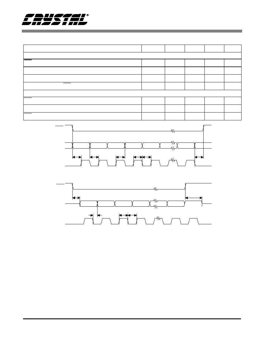
Figure 1. MOSI Write Timing in SPI Slave Mode (Not to Scale)
MISO
SCLK
MSB
MSB - 1
LSB
t
9
t
2
t
1
t
8
t
7
SSI
Figure 2. MISO Read Timing in SPI Slave Mode (Not to Scale)

CS5376
DS256PP1
8
2. GENERAL DESCRIPTION
The CS5376 is a multi-channel digital filter with
integrated system peripherals. The digital decima-
tion filter uses a coefficient programmable signal
processing architecture to filter up to four
-
modulator bit streams. An on-chip reference coef-
ficient set is included to provide an easy set up for
applications that do not require custom digital filter
coefficients.
The CS5376 integrated peripherals simplify system
design by providing a buffered high speed serial
data output port, a test bit stream generator suitable
for driving a test DAC, general purpose I/O pins for
local hardware control, a secondary master mode
SPI port for serial peripherals, and a JTAG port for
boundary scan testing. In addition, a clock and syn-
chronization block synchronizes the CS5376 to the
host system, and a time break controller generates
timing reference information in the output data
stream.
2.1 System Configurations
Coprocessor or Stand-Alone Configurations
Figure 3 illustrates a simplified block diagram of
the CS5376 in a multi-channel system architecture.
This diagram shows the CS5376 in coprocessor
mode, where an external microcontroller operates
as the local host. The microcontroller writes con-
figuration commands and filter coefficients into the
CS5376 from non-volatile memory or from the
communications channel. This system configura-
tion allows the microcontroller to change the filter-
ing function of the CS5376 when instructed to do
so by the system controller.
- Modulators
2
CS5376
Communications
Interface
To
System
Master
CS5372
2
2
2
CS5372
SYNC
CLK
SPI
SD
µC
GPIO
GPIO
GPIO
Modulator
-
Input
Input
Input
Input
Amp
Amp
Amp
Amp
TSBCLK
TSBDATA
MCLK
MSYNC
Figure 3. CS5376 System Level Block Diagram

CS5376
DS256PP1
9
Alternately, the CS5376 can be used in stand-alone
mode, where a configuration EEPROM replaces
the microcontroller. The CS5376 reads configura-
tion commands and filter coefficients directly from
EEPROM, and then enters a fixed operational state.
The stand-alone configuration simplifies system
design by eliminating the CS5376 to microcontrol-
ler interface.
2.2 Digital Filter Description
Multi-Stage Signal Processing Architecture
The CS5376 has a multi-stage signal processing ar-
chitecture consisting of a hardware sinc filter, two
FIR filters, and a selectable 1st, 2nd, or 3rd order
IIR filter. The filter architecture is flexible, with the
capability to bypass later filter stages and output
data immediately following any filter. Figure 4 il-
lustrates the digital filter stages of the CS5376.
The digital filters have decimation ratios that can
achieve data output word rates (OWRs) between
62.5 sps and 4000 sps. Figure 5 lists the standard
OWRs and their associated output periods. Slower
output word rates can be achieved by scaling down
the master clock input.
Programmable or Fixed Coefficients
The CS5376 is designed to load custom filter coef-
ficients and other configuration information via the
SPI 1 serial port from either a microcontroller or a
configuration EEPROM.
The programmed FIR filter coefficients can imple-
ment any type of finite impulse response filter. Lin-
ear phase, minimum phase, phase compensation, or
other complex filter types can be used depending
on the application requirements. The programmed
IIR filter coefficients can implement a 1st, 2nd, or
Figure 4. Digital Filtering Stages
Sinc Filter
16-128
FIR1
4,16
FIR2
2,4
IIR1
IIR2
1st Order
2nd Order
Output to High Speed Serial Data Port (SD Port)
DC Offset
Correction
Output Rate 62.5 Hz ~ 4 kHz
& Gain
Modulator
512 kHz
Input
Figure 5. Digital Filter OWRs
Output Word Rate
Output Period
(OWR)
4000 sps
0.25 ms
2000 sps
0.5 ms
1000 sps
1.0 ms
500 sps
2.0 ms
333.3 sps
3.0 ms
250 sps
4.0 ms
125 sps
8.0 ms
62.5 sps
16.0 ms

CS5376
DS256PP1
10
3rd order infinite impulse response filter with any
corner frequency in the measurement bandwidth.
A set of on-chip FIR and IIR coefficients are in-
cluded in the CS5376 to provide an easy set up for
applications that do not require custom filter coef-
ficients. These coefficients have excellent filtering
characteristics, with the low-pass FIR filters having
a corner frequency at 40% f
s
, in-band ripple less
than ±0.01 dB, and stop-band attenuation greater
than 130 dB. The high-pass IIR filter provides a 3rd
order Butterworth response with a corner frequen-
cy at 2% f
s
.
Programmable Gain and Offset Correction
The final operation of the digital filter is to apply a
user defined gain and offset correction to the output
data. The gain correction value is independently
programmable for each channel and is used to nor-
malize sensor gain across a network. Similarly, the
offset correction is independently programmable
for each channel and is used to correct for DC off-
set in a sensor. The CS5376 also includes a built in
offset calibration routine that will calculate offset
correction values automatically.
2.3 Integrated Hardware Peripherals
High Speed Serial Data Output Port
After filtering is completed, each 24-bit output
sample is combined with an 8-bit status word that
encodes the channel number, a time break flag, and
any error conditions. This 32-bit data word is writ-
ten to an 8-deep FIFO buffer and then transmitted
on request to the communications interface through
the high speed serial data output port. In a typical
system, the communication interface will be a pro-
prietary design.
Test Bit Stream Generator
The CS5376 includes a programmable test bit
stream (TBS) generator that produces a 1-bit
-
modulated bitstream with 24-bits of precision, suit-
able for driving a test DAC to verify the analog per-
formance of the conversion channel. The TBS
generator also includes an internal digital loopback
option so the digital filters and communication in-
terface can be tested independently of the analog
circuitry. The TBS generator can easily be pro-
grammed to produce a number of test signals using
the included 1024 point sine wave data table. By
writing a single configuration register many com-
mon test frequencies can be generated, including
31.25 Hz, 50.0 Hz, and 125.0 Hz. Custom test sig-
nal frequencies can be generated by writing a new
sine wave data table.
Secondary SPI Port
A secondary master mode SPI 2 port allows serial
peripherals to be controlled through the primary
SPI 1 port. The CS5376 acts as an arbiter to con-
duct transactions between the communications in-
terface connected to the primary SPI 1 port and
serial peripherals connected to the secondary SPI 2
port. This simplifies system design by requiring
only one SPI connection to the communication in-
terface to control the CS5376 and multiple serial
peripherals.
General Purpose I/O Pins
Twelve general purpose I/O pins on the CS5376
can be used for local hardware control or as chip se-
lects for the SPI ports. These pins are independent-
ly programmable as inputs or outputs, with or
without an internal pull-up resistor.
JTAG Test Port
The CS5376 includes a standard IEEE 1149.1
JTAG test port for system level testing via bound-
ary scan.
Clock and Synchronization Block
A clock and synchronization block in the CS5376
establishes synchronous timing when used in a dis-
tributed measurement network. An input SYNC
signal from the host system resets the modulator

CS5376
DS256PP1
11
sampling instant, digital filter phase, and test bit-
stream phase to ensure measurement timing is con-
sistent across the network.
Time Break Controller
The CS5376 time break controller places a timing
reference flag in the status bits of the digital filter
output word. This timing reference flag is used to
mark measurement events in the digital data, or as
a digital sync to align multiple data streams during
post-processing. An externally generated TIMEB
signal starts a programmable sample counter (used
to correct for digital filter group delay), and when
it expires the time break flag is set in the next out-
put data word.
2.4 Register Descriptions
Decimation Engine Registers
Hardware functions and digital filter settings in the
CS5376 are controlled by registers in the decima-
tion engine. A summary of decimation engine reg-
isters is shown in Figure 6 on page 12. See
"Decimation Engine Registers" on page 99 for a
detailed listing of all decimation engine register bit
settings.
SPI 1 Registers
Decimation engine registers are not directly acces-
sible to the communication interface. Instead, they
are indirectly read and written using SPI 1 regis-
ters. See "Serial Peripheral Interface 1" on page 21
for a description of how to use the SPI 1 port to ac-
cess decimation engine registers.
Each 24-bit SPI 1 register is divided into three 8-bit
registers consisting of a high, mid, and low byte. A
summary of SPI 1 registers is shown in Figure 6 on
page 12. See "SPI 1 Registers" on page 94 for a de-
tailed listing of all SPI 1 register bit settings.

CS5376
DS256PP1
12
Decimation Engine Registers
SPI 1 Registers
Name
Addr.
Type
# Bits
Description
CONFIG
00
R/W
24
Decimation Engine Configuration
RESERVED
01-0D
R/W
24
Reserved
GPCFG0
0E
R/W
24
GPIO[7:0] Direction, Pullup Enable, and Data
GPCFG1
0F
R/W
24
GPIO[11:8] Direction, Pullup Enable, and Data
SPI2CTRL
10
R/W
24
SPI 2 Configuration
SPI2CMD
11
R/W
16
SPI 2 Command
SPI2DAT
12
R/W
24
SPI 2 Data
RESERVED
13-1F
R/W
24
Reserved
FILT_CFG
20
R/W
24
Filter Configuration
GAIN1
21
R/W
24
Gain Correction Channel 1
GAIN2
22
R/W
24
Gain Correction Channel 2
GAIN3
23
R/W
24
Gain Correction Channel 3
GAIN4
24
R/W
24
Gain Correction Channel 4
OFFSET1
25
R/W
24
Offset Correction Channel 1
OFFSET2
26
R/W
24
Offset Correction Channel 2
OFFSET3
27
R/W
24
Offset Correction Channel 3
OFFSET4
28
R/W
24
Offset Correction Channel 4
TIMEBRK
29
R/W
24
Time Break Counter Configuration
TBS_CFG
2A
R/W
24
Test Bit Stream Configuration
WD_CFG
2B
R/W
24
Watchdog Counter Configuration
SYSTEM1
2C
R/W
24
User Defined System Register 1
SYSTEM2
2D
R/W
24
User Defined System Register 2
VERSION
2E
R/W
24
Hardware Version ID
SELFTEST
2F
R/W
24
Self-Test Result Code
Name
Addr.
Type
# Bits
Description
SPI1CTRL
00 - 02
R/W
8, 8, 8
SPI 1 Control Register
SPI1CMD
03 - 05
R/W
8, 8, 8
DE <-> SPI 1 Command
SPI1DAT1
06 - 08
R/W
8, 8, 8
DE <-> SPI 1 Data 1
SPI1DAT2
09 - 0B
R/W
8, 8, 8
DE <-> SPI 1 Data 2
Figure 6. Decimation Engine and SPI 1 Registers

CS5376
DS256PP1
13
3. SYSTEM DESIGN
System issues to consider when designing with the
CS5376 include power supply voltages, distribu-
tion of clock and synchronization signals, connec-
tions for EEPROM reprogramming, connections
for boundary scan testing, and extra circuitry re-
quired for functional tests.
3.1 Power Supply Voltages
The CS5376 has three sets of power supply inputs.
Two sets supply power to the I/O pins of the chip
(VDD1, VDD2), and the third set supplies power to
the logic core (VD). The I/O pin power supplies de-
termine the maximum input and output voltages
when interfacing to peripherals, and the logic core
power supply determines the power consumption
of the CS5376.
The voltage choice for a specific power supply de-
pends on two considerations.
1) Available voltages.
It's simpler to drive all power supplies from a sin-
gle 5 V or 3.3 V supply if it's already available in
the design. This reduces system cost by eliminating
additional voltage regulators. Power sensitive ap-
plications, however, will require a 3 V supply into
the logic core to minimize power consumption.
2) Required interface voltages.
The two I/O pin power supplies are separated into
a `modulator side' and a `microcontroller side'. If
some elements in the design are specified to inter-
face at 5 V and other elements in the design are
specified to interface at another voltage, 3.3 V for
example, the I/O pin power supplies can be inde-
pendently driven to match.
VDD1, GND1 - Pins 54, 53
This I/O pin power supply sets the interface voltage
to the microcontroller, communications channel,
and related peripherals.
Pins driven by the VDD1 power supply are:
·
RESET, BOOT, CLK, SYNC, TIMEB
·
SSI, SCK1, MOSI, MISO, SINT, SSO
·
SDTKI, SDRDY, SDCLK, SDDAT, SDTKO
·
GPIO6 - GPIO11
·
TRST, TMS, TCK, TDI, TDO
VDD2, GND2 - Pins 11, 25, 24, 38
This I/O pin power supply sets the interface voltage
to the modulators, test DAC, and related peripher-
als.
Pins driven by the VDD2 power supply are:
·
MDATA1 - MDATA4, MFLAG1 - MFLAG4
·
MCLK, MCLK/2, MSYNC
·
SCK2, SI1 - SI4, SO
·
TBSCLK, TBSDATA
·
GPIO0 - GPIO5
VD, GND - Pins 7, 40, 6, 23, 39
This power supply sets the operational voltage for
the CS5376 logic core. Lowering this voltage to
3 V will minimize power consumption.
3.1.1
Bypass Capacitors
All power supply pins should be bypassed to pro-
vide noise immunity. The bypass capacitors should
be placed as close as possible to the pins of the
CS5376, between the power supply pin and its as-
sociated ground. Suggested values for bypass ca-
pacitors are two parallel caps of 1
µF and 0.01 µF,
or a single cap of 0.1
µF. Bypass capacitors can be
ceramic, tantalum, or any other dielectric type.
3.2 Clock and Synchronization Signals
Many applications of the CS5376 will use a multi-
channel distributed measurement network. To be
useful, data collection must occur with synchro-
nous timing between the measurement channels.

CS5376
DS256PP1
14
Careful design of a clock distribution and synchro-
nization network is crucial for keeping these timing
relationships consistent.
CLK - Pin 58
The CS5376 master clock pin, CLK, has a nominal
input frequency of 32.768 MHz. A slower master
clock can be used if the frequencies from the gen-
erated clocks (MCLK, MCLK/2, SCK1, SCK2,
and TBSCLK) are permitted to run slower. The
CS5376 is a fully static design and can have the
master clock gated off to place the system in a low-
power standby mode.
3.2.1
Master Clock Jitter and Skew
The clock distribution network should supply a
low-jitter, low-skew master clock signal. Clock jit-
ter on the master clock pin, CLK, will result in jitter
on all generated clocks. Jitter on the modulator
clocks (MCLK, MCLK/2) and the test bit stream
clock (TBSCLK) will cause inaccurate conversions
of analog-to-digital and digital-to-analog signals.
Great care should be taken to ensure recovered
clocks have as low jitter as possible.
Clock skew across a measurement network will
cause inaccurate results when reconstructing mea-
surement data during post-processing. By making
measurements at slightly different instants in time,
sensors with clock skew between them cause sig-
nals to appear slower or faster than reality. A good
measurement network design should minimize
clock skew.
3.2.2
Synchronization Jitter and Skew
Similar problems face the distribution of the SYNC
signal. The SYNC input on the CS5376 aligns the
internal clock edges and digital filter phase to the
external system, establishing a precise timing rela-
tionship across the measurement network. Jitter
and skew on the input SYNC signal will result in
phase errors in the CS5376 digital filter data.
The SYNC signal is also used to generate the
MSYNC signal to the modulators. The MSYNC
signal synchronizes the modulator sampling instant
and ensures all modulators are operating with iden-
tical timing across the network. Since the sampling
instant is defined by the MSYNC signal, errors
generating the SYNC signal will result in measure-
ment timing errors by the modulators.
See "System Synchronization" on page 77 for
more information on synchronizing the CS5376
measurement system.
3.3 EEPROM Programming
The CS5376 in stand-alone mode automatically
boots from EEPROM after reset. The configuration
EEPROM holds the commands and data needed to
initialize the system into a fixed operational state.
If stand-alone boot mode is used, the system should
include a way to address the configuration EE-
PROM for in-circuit reprogramming. This can be
performed locally by a technician through a con-
nector, or remotely through the communications
channel.
See "Serial Peripheral Interface 1" on page 21 for
more information about booting the CS5376 using
an EEPROM.
3.4 Boundary Scan Testing
During system design and in the field, in-circuit
testing is a valuable diagnostic tool. The CS5376
JTAG test port enables boundary scan testing by
providing access to all pins via internal boundary
scan cells. To use the JTAG test port, a system de-
sign must provide in-circuit access to the CS5376
JTAG pins (TRST, TMS, TCK, TDI, and TDO).
They can be accessed locally by a technician
through a connector, or remotely through the com-
munications channel.
See "JTAG Test Port (IEEE 1149.1)" on page 89
for more information on the JTAG test port.

CS5376
DS256PP1
15
3.4.1
TRST and RESET Pins
As required by the IEEE 1149.1 specification, the
JTAG reset signal, TRST, is independent of the
CS5376 reset signal, RESET. The status of the
TRST pin should be considered during system de-
sign since the TAP controller must be reset before
using the JTAG port.
In systems not using the JTAG test port, the TRST
pin can be connected directly to the RESET pin, or
can be connected to ground. In systems using the
JTAG test port, the TRST and RESET pins should
be independently driven to provide reset capability
during boundry scan.
3.5 Functional Testing
While boundary scan testing gives the ability to
check connections between circuit elements, test-
ing the functionality of the circuit elements them-
selves requires operation of the measurement
channel.
3.5.1
Analog Test DAC
To test the full signal path of a CS5376 system, an
analog test signal should be applied to the modula-
tor inputs. The CS5376 provides a test bit stream
generator that produces a
- bit stream suitable
for driving an external test DAC. The analog output
signal from the DAC can be multiplexed to the in-
puts of the measurement channel through relays or
analog multiplexers. Switching the analog test sig-
nal into the measurement channel is typically per-
formed on command from the communication
channel, and requires appropriate control signals to
be defined during system design.
Included as part of the CS5376 test bit stream gen-
erator is an internal feedback path into the digital
filters. This loopback mode provides a fully digital
signal path to test the digital filters and communi-
cations interface. If this is the only test mode used,
no external circuitry is required.
See "Test Bit Stream Generator" on page 81 for
more information about using the test bit stream
generator.
3.5.2
Step Input and Group Delay
Characterizing the step response of a combination
analog and digital measurement channel can be dif-
ficult. A simple method to empirically measure the
step response and group delay through the analog
and digital portions of a CS5376 measurement
channel is to use the time break signal as both a tim-
ing reference and an analog step input. This test re-
quires the system design to include relays or analog
multiplexers to connect the time break signal to the
analog inputs.
See "Time Break Function" on page 75 for more
information about the time break signal.
3.6 System Registers
Several registers are included in the CS5376 for
system information.
The VERSION register (0x2E) in the decimation
engine holds hardware version ID information.
Two registers in the decimation engine, SYSTEM1
and SYSTEM2 (0x2C, 0x2D), are provided for
user defined system information. These are general
purpose registers and will hold any 24-bit data val-
ues written to them.

CS5376
DS256PP1
16
3.6.1
VERSION Register - 0x2E
(MSB) 23
22
21
20
19
18
17
16
TYPE7
TYPE6
TYPE5
TYPE4
TYPE3
TYPE2
TYPE1
TYPE0
R/W
R/W
R/W
R/W
R/W
R/W
R/W
R/W
0
1
1
1
0
1
1
0
15
14
13
12
11
10
9
8
HW7
HW6
HW5
HW4
HW3
HW2
HW1
HW0
R/W
R/W
R/W
R/W
R/W
R/W
R/W
R/W
0
0
0
0
0
0
0
1
7
6
5
4
3
2
1
(LSB) 0
ROM7
ROM6
ROM5
ROM4
ROM3
ROM2
ROM1
ROM0
R/W
R/W
R/W
R/W
R/W
R/W
R/W
R/W
0
0
0
0
0
0
0
1
I/O Address: 0x2E
--
Not defined;
read as 0
R
Readable
W
Writable
R/W
Readable and
Writable
Bits in bottom rows
are reset condition
Figure 7. Hardware Version ID Register VERSION
Bit definitions:
23:16 TYPE
[7:0]
Chip Type
76 - CS5376
15:8
HW
[7:0]
Hardware Revision
01 - Rev A
7:4
ROM
[7:0]
ROM Version
01 - Ver 1.0

CS5376
DS256PP1
17
3.6.2
SYSTEM1, SYSTEM2 Registers - 0x2C, 0x2D
(MSB) 23
22
21
20
19
18
17
16
SYS23
SYS22
SYS21
SYS20
SYS19
SYS18
SYS17
SYS16
R/W
R/W
R/W
R/W
R/W
R/W
R/W
R/W
0
0
0
0
0
0
0
0
15
14
13
12
11
10
9
8
SYS15
SYS14
SYS13
SYS12
SYS11
SYS10
SYS9
SYS8
R/W
R/W
R/W
R/W
R/W
R/W
R/W
R/W
0
0
0
0
0
0
0
0
7
6
5
4
3
2
1
(LSB) 0
SYS7
SYS6
SYS5
SYS4
SYS3
SYS2
SYS1
SYS0
R/W
R/W
R/W
R/W
R/W
R/W
R/W
R/W
0
0
0
0
0
0
0
0
I/O Address: 0x2C
--
Not defined;
read as 0
R
Readable
W
Writable
R/W
Readable and
Writable
Bits in bottom rows
are reset condition
Figure 8. User Defined System Register SYSTEM1
Bit definitions:
23:16 SYS[23:16]
System Register
Upper Byte
15:8
SYS[15:8]
System Register
Middle Byte
15:8
SYS[7:0]
System Register
Lower Byte

CS5376
DS256PP1
18
4. RESET CONTROL
When the RESET signal is released, the CS5376
automatically performs a series of self-tests. De-
pending on the state of the BOOT pin, it then either
actively boots from EEPROM or waits for config-
uration information to be written by a microcon-
troller.
4.1 Reset Pin Descriptions
RESET - Pin 55
RESET is an active low signal that places the
CS5376 into a reset state when asserted.
BOOT - Pin 56
The BOOT signal selects how the CS5376 loads
configuration information. The logic state of this
pin is latched 1
µs after RESET is released to select
between coprocessor or stand-alone boot modes. A
logical low selects coprocessor boot mode, a logi-
cal high selects stand-alone boot mode.
4.2 Boot Configurations
When booting in coprocessor mode, a microcon-
troller or other SPI bus master is required to write
configuration information. When booting in stand-
alone mode, the CS5376 reads configuration infor-
mation from EEPROM and no microcontroller is
required. A hybrid mode can also be used which
reads an initial configuration from EEPROM and
then writes changes using a microcontroller.
Coprocessor Mode
Coprocessor mode is designed for systems required
to run multiple configurations from a common set
of hardware. The ability to change configurations
in real time gives maximum flexibility in the field.
This mode requires a microcontroller or other SPI
bus master to be connected to the CS5376 SPI 1
port. The microcontroller can rewrite the filter co-
efficients, change the filter output stage, enable and
disable the test bit stream, and manually update the
gain and offset correction values during operation.
To set the CS5376 configuration, the microcontrol-
ler writes a series of command and data values to
the decimation engine through the SPI 1 port. See
"Serial Peripheral Interface 1" on page 21 for more
information on connecting a microcontroller to the
SPI 1 port.
Stand-Alone Mode
If the CS5376 is designed into a system with a fixed
configuration, no microcontroller is required.
Stand-alone mode boots from EEPROM to a fixed
configuration and immediately begins operation.
The EEPROM contains all configuration informa-
tion including filter coefficients, register settings,
and test bit stream data.
It might not be possible to know the gain and offset
correction values in advance of deploying a system.
If the configuration EEPROM is in-circuit repro-
grammable, the system can be booted with offset
and gain correction disabled and the appropriate
correction values calculated. The new correction
values can then be programmed into the EEPROM
and the CS5376 re-booted with gain and offset cor-
rection enabled.
See "Serial Peripheral Interface 1" on page 21 for
more information on booting from a configuration
EEPROM, and the format required for EEPROM
data.
Hybrid Mode
A boot configuration that requires more engineer-
ing effort to implement is a hybrid
coprocessor / stand-alone boot mode. In hybrid
mode the CS5376 initially boots in stand-alone
mode from a configuration EEPROM. After boot-
ing, a microcontroller updates the configuration in-
formation in coprocessor mode by writing
commands to the decimation engine through the
SPI 1 port.
Hybrid mode is more complex at the system level
because it requires the ability to tri-state the micro-

CS5376
DS256PP1
19
controller to SPI 1 connection during the initial EE-
PROM boot. After the initial configuration is
loaded, the microcontroller seizes control of the
SPI 1 port and updates the configuration as re-
quired. The EEPROM will not interfere with mi-
crocontroller to SPI 1 transactions provided the
initial stand-alone boot was completed.
Updated configuration information from the micro-
controller can not be written until the EEPROM
boot loader has relinquished control of the SPI 1
port. To guarantee this, the microcontroller should
monitor the CS5376 CS11 / GPIO11 pin into the
EEPROM for inactivity, or simply wait the maxi-
mum time required to boot from EEPROM. The re-
quired boot time from EEPROM depends on the
number of coefficients written, the number of reg-
isters written, and if test bit stream data is written.
A final requirement for hybrid boot mode is the
ability to address both the CS5376 and the config-
uration EEPROM. When writing to the CS5376
SPI 1 port, serial transactions use an 8-bit address.
Supported serial EEPROMs, however, require seri-
al transactions to use 16-bit addressing. If a micro-
controller is to interface with the CS5376 and also
be able to in-circuit reprogram the configuration
EEPROM, the serial port connection must support
both addressing modes.
See "Serial Peripheral Interface 1" on page 21 for
information about connections to the SPI 1 port,
the format required for EEPROM data, and the
SPI 1 commands available for updating the config-
uration.
4.3 Reset Self-Tests
After the reset signal is de-asserted but before the
CS5376 starts the boot operation, a series of self
test are run. These tests check the operation of the
decimation engine and report pass/fail codes in the
SELFTEST register (0x2F). The full suite of self
tests require approximately 60ms to complete.
Program ROM Test
This self-test calculates a checksum from the con-
tents of program ROM and compares against an ex-
pected value. The result of this test is 0x00000A if
passed or 0x00000F if failed.
Data ROM Test
This self-test calculates a checksum from the con-
tents of data ROM and compares against an expect-
ed value. The result of this test is 0x0000A0 if
passed or 0x0000F0 if failed.
Program RAM Test
This self-test writes a series of patterns into the pro-
gram RAM and compares against expected read
values. The result of this test is 0x000A00 if passed
or 0x000F00 if failed.
Data RAM Test
This self-test writes a series of patterns into the data
RAM and compares against expected read values.
The result of this test is 0x00A000 if passed or
0x00F000 if failed.
Execution Unit Test
This self-test exercises the execution unit with a se-
quence of calculations, comparing against expect-
ed values. The result of this test is 0x0A0000 if
passed or 0x0F0000 if failed.

CS5376
DS256PP1
20
4.3.1
SELFTEST Register - 0x2F
(MSB) 23
22
21
20
19
18
17
16
--
--
--
--
EU3
EU2
EU1
EU0
R/W
R/W
R/W
R/W
R/W
R/W
R/W
R/W
0
0
0
0
1
0
1
0
15
14
13
12
11
10
9
8
DRAM3
DRAM2
DRAM1
DRAM0
PRAM3
PRAM2
PRAM1
PRAM0
R/W
R/W
R/W
R/W
R/W
R/W
R/W
R/W
1
0
1
0
1
0
1
0
7
6
5
4
3
2
1
(LSB) 0
DROM3
DROM2
DROM1
DROM0
PROM3
PROM2
PROM1
PROM0
R/W
R/W
R/W
R/W
R/W
R/W
R/W
R/W
1
0
1
0
1
0
1
0
I/O Address: 0x2F
--
Not defined;
read as 0
R
Readable
W
Writable
R/W
Readable and
Writable
Bits in bottom rows
are reset condition
Figure 9. Self Test Result Register SELFTEST
Bit definitions:
23:20 --
reserved
15:12 DRAM
[3:0]
Data RAM Test
`A': Pass
`F': Fail
7:4
DROM
[3:0]
Data ROM Test
`A': Pass
`F': Fail
19:16 EU
[3:0]
Execution Unit Test
`A': Pass
`F': Fail
11:8
PRAM
[3:0]
Program RAM Test
`A': Pass
`F': Fail
3:0
PROM
[3:0]
Program ROM Test
`A': Pass
`F': Fail

CS5376
DS256PP1
21
5. SERIAL PERIPHERAL INTERFACE 1
The Serial Peripheral Interface 1 (SPI 1) port is an
industry standard master / slave SPI interface, and
is the primary interface to the CS5376 decimation
engine. The port operates as an SPI bus master
when booting from a configuration EEPROM in
stand-alone mode, and as an SPI slave when com-
municating with a microcontroller in coprocessor
mode.
Master Mode
The SPI 1 port operates in master mode only while
loading configuration information from EEPROM
during stand-alone boot mode. In this mode the
CS5376 actively initiates serial transactions to read
configuration register values, digital filter coeffi-
cients, and test bit stream data from EEPROM
memory. After booting from EEPROM, the SPI 1
port reverts to slave mode to interface with a micro-
controller, if present.
Master mode serial transactions in the CS5376 gen-
erate a chip select output on the CS11 / GPIO11
pin, and a serial clock output on the SCK1 pin. Se-
rial data is output from the CS5376 on the MOSI
pin, and input from the EEPROM on the MISO pin.
To be compatible with many serial EEPROMs,
transactions in master mode use 16-bit addresses,
different from the 8-bit addresses required when
accessing the CS5376 in slave mode.
Slave Mode
When booting from a microcontroller in coproces-
sor mode, or after booting from EEPROM in stand-
alone mode has completed, the SPI 1 port operates
in slave mode. In slave mode the CS5376 is pas-
sive, with serial transactions initiated by a micro-
controller or other SPI bus master. The
microcontroller uses SPI 1 commands to write con-
figuration register values, digital filter coefficients,
and test bit stream data from a local memory or
from the communications channel.
Slave mode serial transactions require the micro-
controller to use the SSI pin as the CS5376 chip se-
lect, and to generate a serial clock input on the
SCK1 pin. Serial data is received from the micro-
controller on the MOSI pin, and output from the
CS5376 on the MISO pin.
When pulled low the SSI pin (Slave Select Input)
places the SPI 1 port into a default configuration
that requires 8-bit addresses, different from the 16-
SCK1
MISO
MOSI
Pin Logic
SPI 1
Figure 10. Serial Peripheral Interface 1 (SPI 1) Block Diagram
SINT
To
8-bit Shift Register
SSI
SSO
Chip
Select
Logic
Control Logic
CS8
CS10
CS9
CS11
Registers
Engine
Decimation
SPI 1

CS5376
DS256PP1
22
bit addresses generated when accessing an EE-
PROM in master mode.
5.1 SPI 1 Pin Descriptions
The Serial Peripheral Interface 1 port is a standard
3-wire, bidirectional, synchronous serial interface.
The SCK1, MISO, and MOSI pins, along with ei-
ther the CS11 or SSI chip select pins, are used to in-
terface the decimation engine of the CS5376 to
external serial devices. Several miscellaneous pins,
SINT, SSO, and CS8 - CS10 are not used but are
defined to make the SPI 1 port extensible in the fu-
ture.
CS11 - Pin 46
Master mode chip select output pin, active low. EE-
PROM chip select signal automatically generated
when booting in stand-alone mode.
SSI - Pin 49
Slave mode chip select input pin, active low. Chip
select signal that places the SPI 1 port into slave
mode to receive commands from a microcontroller.
SCK1 - Pin 48
Master mode serial clock output, slave mode serial
clock input. In both modes a serial clock rising
edge indicates valid data, a falling edge indicates a
data transition.
In master mode the SCK1 pin is an output that gen-
erates a serial clock to read data from the configu-
ration EEPROM. The serial clock output rate in
master mode defaults to 1.024 MHz.
In slave mode the SCK1 pin is an input that re-
ceives a serial clock from a microcontroller. The
serial clock input rate in slave mode can be any rate
up to a maximum of 4.096 MHz.
MOSI - Pin 51
Master Out, Slave In data pin. Data output in mas-
ter mode, data input in slave mode. Data is valid on
the rising edge of SCK1, and transitions on the fall-
ing edge.
MISO - Pin 50
Master In, Slave Out data pin. Data input in master
mode, data output in slave mode. Data is valid on
the rising edge of SCK1, and transitions on the fall-
ing edge.
SINT - Pin 52
SPI 1 interrupt output pin, active low. A pulsed
output indicates data was written to the SPI 1 reg-
isters by the decimation engine. Not used by
CS5376 rev A, reserved for future revisions.
SSO - Pin 47
Slave select output pin, active low. Chip select out-
put that mirrors the SSI pin. Not used by CS5376
rev A, reserved for future revisions.
CS8 - CS10 - Pins 43 - 46
Additional chip selects for SPI 1 master mode. Not
used by CS5376 rev A, reserved for future revi-
sions.
5.2 SPI 1 Stand-Alone Mode
In stand-alone mode, the SPI 1 port operates as an
SPI bus master to load configuration information
from an EEPROM. Commands to write configura-
tion registers, filter coefficients, and test bit stream
data are programmed into the EEPROM along with
the required data words.
The CS5376 automatically reads 1-byte command
and 3-byte data words from EEPROM memory un-
til the `Filter Start' command is received. The `Fil-
ter Start' command initializes the CS5376 digital
filters and places the SPI 1 port into slave mode.
See "SPI 1 Coprocessor Mode" on page 27 for
more information about SPI 1 slave mode.

CS5376
DS256PP1
23
5.2.1
EEPROM Organization
The configuration EEPROM is programmed with a
series of command and data values. Commands are
one byte (8-bit) values that select the type of EE-
PROM loader operation. Data words are three byte
(24-bit) values used by the EEPROM loader.
The CS5376 expects EEPROM programming to
start at memory location 0x10, with the bytes from
0x00 to 0x0F defined for manufacturing header in-
formation. The first CS5376 to EEPROM transac-
tion reads a 1-byte command from memory
location 0x10. Depending on the command type,
multiple 3-byte data words are read to complete the
command. The CS5376 continues reading com-
mand and data values until the `Filter Start' com-
mand is recognized. Figure 11 illustrates the
organization of an 8 Kbyte (64 Kbit) configuration
EEPROM.
The maximum data that can be written for a single
configuration is approximately 5 Kbyte (40 Kbit),
which includes command overhead:
-
22 Configuration Registers, 154 bytes
-
255 + 255 FIR Coefficients, 1537 bytes
-
3 + 5 IIR Coefficients, 25 bytes
-
1024 Test Bit Stream Data, 3076 bytes
-
Filter Start Command, 1 byte
Supported serial configuration EEPROMs are
SPI mode 0 (0,0) compatible, 16-bit addresses, 8-
bit data, and larger than 5 Kbyte. ATMEL
AT25640, AT25128, or similar serial EEPROMs
are recommended.
5.2.2
EEPROM Commands
The configuration EEPROM contains a series of 1-
byte command and 3-byte data words. After an EE-
PROM command is read, multiple data words are
read to complete the programmed operation. Not
all EEPROM commands require additional data
words.
EEPROM commands can write decimation engine
registers, write FIR filter coefficients, write IIR fil-
ter coefficients, write test bitstream data, and start
the digital filters. A summary of available EE-
PROM commands is shown in Figure 12 on
page 24.
Write Register - 0x01
This EEPROM command writes a data value to the
specified decimation engine register. Decimation
engine registers control hardware and filtering
functions. See "Decimation Engine Registers" on
page 99 for information about the bit definitions of
the decimation engine registers.
Figure 11. EEPROM Memory Organization
0000h
1FFFh
EEPROM
Manufacturing
Information
EEPROM
Command and
Data Values
Mfg Header
8 bit Command
0010h
N x 24 bit Data
8 bit Command
N x 24 bit Data
8 bit Command
N x 24 bit Data
. . .
Type
Description
CMD
0x01 - Register Write Command
DATA
Register Address
DATA
Register Write Data

CS5376
DS256PP1
24
Write FIR Coefficients - 0x02
This EEPROM command writes custom coeffi-
cients for the FIR1 and FIR2 filters. The first two
data words set the number of FIR1 and FIR2 coef-
ficients to be written. The remaining data words are
the concatenated FIR1 and FIR2 coefficients.
A maximum of 255 coefficients can be written for
each FIR filter, though the available decimation en-
gine computation cycles will limit their practical
size. See "FIR Filters" on page 60 for more infor-
mation about the FIR filters and the cycle limita-
tions of the decimation engine.
Type
Description
CMD
0x02 - FIR Coefficient Write Cmd
DATA
Number of FIR1 Coefficients
DATA
Number of FIR2 Coefficients
DATA
(FIR Coefficients)
EEPROM Command
Command Opcode
Data Format
1
Nop
0x00
--
Write I/O Register
0x01
Address
Write Data
Write FIR Coefficients
0x02
Num FIR1 Coeff
Num FIR2 Coeff
(FIR Coeff)
Write IIR Coefficients
0x03
(IIR Coeff)
Write ROM Coefficients
0x04
--
Write TBS Data
0x05
Num TBS Data
(TBS Data)
Write ROM TBS Data
0x06
--
Filter Start
0x07
--
Figure 12. EEPROM Boot Loader Commands
1
(data) indicates multiple data words of this type to be written.

CS5376
DS256PP1
25
Write IIR Coefficients - 0x03
This EEPROM command uploads custom coeffi-
cients for the two stage IIR filter. The IIR architec-
ture and number of coefficients is fixed, so eight
data words containing coefficient values immedi-
ately follow the command byte. The IIR coefficient
write order is: a11, b10, b11, a21, a22, b20, b21,
and b22.
The IIR filter consists of a 1st order filter requiring
three coefficients (a11, b10, b11) and a 2nd order
filter requiring five coefficients (a21, a22, b20,
b21, b22). A 3rd order filter is implemented by run-
ning both the 1st and 2nd order filters. See "IIR Fil-
ter" on page 61 for more information about the IIR
filter.
Write ROM Coefficients - 0x04
This EEPROM command writes the on-chip refer-
ence coefficients for FIR1, FIR2, IIR 1st order, and
IIR 2nd order filters for use by the decimation en-
gine. No data words are required for this EEPROM
command. See "Reference Coefficients" on
page 63 for more information about the reference
FIR and IIR coefficient sets.
Write TBS Data - 0x05
This EEPROM command uploads a custom data
set for the test bit stream (TBS) generator. The first
data word sets the number of TBS data to be written
and the remaining data words are the TBS data val-
ues.
This command, along with the ability to program
the test bit stream generator interpolation and clock
rate, allows the creation of custom frequency test
signals. See "Test Bit Stream Generator" on
page 81 for information on generating specific test
frequencies using custom test bit stream data sets.
Write ROM TBS Data - 0x06
This EEPROM command writes the on-chip test bit
stream (TBS) data for use by the TBS generator.
No data words are required for this EEPROM com-
mand. See "Test Bit Stream Generator" on page 81
for information on generating test frequencies us-
ing the on-chip test bit stream data set.
Filter Start - 0x07
This EEPROM command initializes the decimation
engine and starts the digital filters. It also ends the
EEPROM boot loader operation and places the
SPI 1 port into slave mode. No data words are re-
quired for this EEPROM command.
After receiving the Filter Start command, the deci-
mation engine uses the filter configuration speci-
fied in the FILT_CFG register (0x20) and filter
Type
Description
CMD
0x03 - IIR Coefficient Write Cmd
DATA
IIR Coefficient a11
DATA
IIR Coefficient b10
DATA
IIR Coefficients b11
DATA
IIR Coefficients a21
DATA
IIR Coefficients a22
DATA
IIR Coefficients b20
DATA
IIR Coefficients b21
DATA
IIR Coefficients b22
Type
Description
CMD
0x04 - ROM Coefficient Write Cmd
Type
Description
CMD
0x05 - TBS Data Write Cmd
DATA
Number of TBS Data
DATA
(TBS Data)
Type
Description
CMD
0x06 - TBS ROM Data Write Cmd
Type
Description
CMD
0x07 - Filter Start Command

CS5376
DS256PP1
26
coefficients specified by prior EEPROM com-
mands.
5.2.3
CS5376 to EEPROM Transactions
When reading data from EEPROM in stand-alone
boot mode, the SPI 1 port operates as a bus master.
Two types of serial transactions are generated by
the CS5376, command reads and data reads. Com-
mand reads are 4-byte serial transactions to read a
command byte, and data reads are 6-byte serial
transactions to read a data word. Master mode
CS5376 to EEPROM transaction timing is shown
in Figure 13.
Command Read Transactions
A CS5376 to EEPROM command read transaction
reads a 1-byte command from EEPROM memory.
It requires a 4-byte serial transaction to complete: a
1-byte SPI `read' opcode (0x03), a 2-byte EE-
PROM address, and the returned 1-byte command
value. Based on the returned command value, the
SCK1
MOSI
CS11
MSB
LSB
MISO
X
6
1
2
3
4
5
MSB
LSB
6
1
2
3
4
5
1
8
2
7
6
5
4
3
Cycle
MOSI
MISO
SSI
0x03
ADDR
DATA1
DATA3
DATA2
CS11
READ
1 BYTE / 3 BYTE
ADDR
CMD
ADDR
DATA
2 BYTE
Figure 13. SPI 1 Master Mode Transactions
SPI 1 Read from EEPROM

CS5376
DS256PP1
27
CS5376 initiates multiple data read transactions to
complete the command.
The CS5376 initiates a command read transaction
by pulling the CS11 / GPIO11 pin low to act as the
EEPROM chip select. It then writes serial clocks to
the SCK1 pin, writes the SPI `read' opcode and EE-
PROM address to the MOSI pin, and reads the re-
turned command value from the MISO pin. All
MOSI and MISO data are shifted MSB first, with
data valid on the rising edge of SCK1 and transi-
tioning on the falling edge.
Data Read Transactions
A CS5376 to EEPROM data read transaction reads
a 3-byte data word from EEPROM memory. It re-
quires a 6-byte serial transaction to complete: a 1-
byte SPI `read' opcode (0x03), a 2-byte EEPROM
address, and the returned 3-byte data value. De-
pending on the command type, the CS5376 initiates
multiple data reads to complete it.
The CS5376 initiates a data read transaction by
pulling the CS11 / GPIO11 pin low to act as the
EEPROM chip select. It then writes serial clocks to
the SCK1 pin, writes the SPI `read' opcode and EE-
PROM address to the MOSI pin, and reads the re-
turned data value from the MISO pin. All MOSI
and MISO data are shifted MSB first, with data val-
id on the rising edge of SCK1 and transitioning on
the falling edge.
5.3 SPI 1 Coprocessor Mode
In coprocessor mode the CS5376 operates as an
SPI slave. A microcontroller or other SPI bus mas-
ter initiates serial transactions to the SPI 1 port to
write configuration information and start the digital
filters. Coprocessor mode is the most flexible
method of configuring the CS5376 since it permits
real time changes to the measurement setup.
The CS5376 digital filters and embedded test func-
tions are configured by writing command and data
values to the decimation engine. The decimation
engine is not directly addressable through the SPI 1
port, but instead the command and data values are
written indirectly through a set of SPI 1 registers.
Available SPI 1 coprocessor mode commands can
read or write the decimation engine registers, write
digital filter coefficients, write test bit stream data,
and enable or disable the digital filters.
5.3.1
SPI 1 Registers
Coprocessor mode commands are invoked by writ-
ing command and data values to a set of SPI 1 reg-
isters. The SPI1CTRL, SPI1CMD, SPI1DAT1, and
SPI1DAT2 registers are 24-bit registers mapped
into an 8-bit register space as high, mid, and low
bytes.
SPI 1 registers are separate from decimation engine
registers, with only SPI 1 registers directly addres-
sable by a microcontroller or other SPI bus master.
Decimation engine registers are read or written
with the `Read Register' or `Write Register' SPI 1
commands.
Name
Addr.
Type
# Bits
Description
SPI1CTRLH
00 - 02
R/W
8, 8, 8
SPI 1 Control Register
SPI1CMDH
03 - 05
R/W
8, 8, 8
DE <-> SPI 1 Command
SPI1DAT1H
06 - 08
R/W
8, 8, 8
DE <-> SPI 1 Data 1
SPI1DAT2H
09 - 0B
R/W
8, 8, 8
DE <-> SPI 1 Data 2
Figure 14. SPI 1 Register Space

CS5376
DS256PP1
28
5.3.2
SPI1CTRL Register
(MSB) 23
22
21
20
19
18
17
16
--
--
SCK1PO
SCK1PH
WOM
SCK1FS2
SCK1FS1
SCK1FS0
R/W1
R/W1
R/W
R/W
R/W
R/W
R/W
R/W
0
0
0
0
1
0
1
1
15
14
13
12
11
10
9
8
SMODF
PROM
DEOP
EMOP
SWEF
SINT
IEN
E2DREQ
R
R/W
R
R
R
R/W
R/W
R/W
0
0
0
0
0
0
0
0
7
6
5
4
3
2
1
(LSB) 0
DNUM2
DNUM1
DNUM0
CS11
CS10
CS9
CS8
D2SREQ
R/W
R/W
R/W
R/W
R/W
R/W
R/W
R/W
0
0
1
0
0
0
0
0
SPI 1 Address: 0x00
0x01
0x02
--
Not defined;
read as 0
R
Readable
W
Writable
R/W
Readable and
Writable
Bits in bottom rows
are reset condition
Bit definitions:
23:22 --
reserved
15
SMODF
SPI 1 mode fault error
7:5
DNUM
[2:0]
DE number of bytes in
transaction (1-8 or 2-9)
21
SCK1PO SCK1 polarity
1: On falling edge
0: On rising edge
14
PROM
PROM mode
1: 2-byte address
0: 1-byte address
4
CS11
SPI 1 chip select 11
20
SCK1PH SCK1 phase
1: Data out at first SCK1
edge
0: Data out before first
SCK1 edge
13
DEOP
DE to SPI 1 operation in
progress
3
CS10
SPI 1 chip select 10
19
WOM
Wired-OR logic
1: Enabled (open drain)
0: Disabled (push-pull)
12
EMOP
External master to SPI 1
operation in progress
2
CS9
SPI 1 chip select 9
18:16 SCK1FS
[2:0]
SCK1 output freq.
111: reserved
110: reserved
101: 4.096 MHz
100: 2.048 MHz
011: 1.024 MHz
(default)
010: 512 kHz
001: 256 kHz
000: 32 kHz
11
SWEF
SPI 1 write collision
error flag
1
CS8
SPI 1 chip select 8
10
SINT
Serial Interrupt
0
D2SREQ DE to SPI request
1: Request operation
0: Operation done
(cleared by SPI)
9
IEN
SPI 1 Interrupt enable
8
E2DREQ External master to DE
request
Figure 15. SPI Control Register SPI1CTRL

CS5376
DS256PP1
29
5.3.3
SPI1CMD Register
(MSB) 23
22
21
20
19
18
17
16
S1CMD23
S1CMD22
S1CMD21
S1CMD20
S1CMD19
S1CMD18
S1CMD17
S1CMD16
R/W
R/W
R/W
R/W
R/W
R/W
R/W
R/W
0
0
0
0
0
0
0
0
15
14
13
12
11
10
9
8
S1CMD15
S1CMD14
S1CMD13
S1CMD12
S1CMD11
S1CMD10
S1CMD9
S1CMD8
R/W
R/W
R/W
R/W
R/W
R/W
R/W
R/W
0
0
0
0
0
0
0
0
7
6
5
4
3
2
1
(LSB) 0
S1CMD7
S1CMD6
S1CMD5
S1CMD4
S1CMD3
S1CMD2
S1CMD1
S1CMD0
R/W
R/W
R/W
R/W
R/W
R/W
R/W
R/W
0
0
0
0
0
0
0
0
SPI 1 Address: 0x03
0x04
0x05
--
Not defined;
read as 0
R
Readable
W
Writable
R/W
Readable and
Writable
Bits in bottom rows
are reset condition
Figure 16. SPI 1 Command Register SPI1CMD
Bit definitions:
23:16 S1CMD[23:16] SPI 1 Command
High Byte
15:8
S1CMD[15:8] SPI 1 Command
Middle Byte
15:8
S1CMD[7:0] SPI 1 Command Low
Byte

CS5376
DS256PP1
30
5.3.4
SPI1DAT1 Register
(MSB) 23
22
21
20
19
18
17
16
S1DAT23
S1DAT22
S1DAT21
S1DAT20
S1DAT19
S1DAT18
S1DAT17
S1DAT16
R/W
R/W
R/W
R/W
R/W
R/W
R/W
R/W
0
0
0
0
0
0
0
0
15
14
13
12
11
10
9
8
S1DAT15
S1DAT14
S1DAT13
S1DAT12
S1DAT11
S1DAT10
S1DAT9
S1DAT8
R/W
R/W
R/W
R/W
R/W
R/W
R/W
R/W
0
0
0
0
0
0
0
0
7
6
5
4
3
2
1
(LSB) 0
S1DAT7
S1DAT6
S1DAT5
S1DAT4
S1DAT3
S1DAT2
S1DAT1
S1DAT0
R/W
R/W
R/W
R/W
R/W
R/W
R/W
R/W
0
0
0
0
0
0
0
0
SPI 1 Address: 0x06
0x07
0x08
--
Not defined;
read as 0
R
Readable
W
Writable
R/W
Readable and
Writable
Bits in bottom rows
are reset condition
Figure 17. SPI 1 Data Register SPI1DAT1
Bit definitions:
23:16 S1DAT[23:16] SPI 1 Data 1 High
Byte
15:8
S1DAT[15:8] SPI 1 Data 1 Middle
Byte
15:8
S1DAT[7:0]
SPI 1 Data 1 Low
Byte
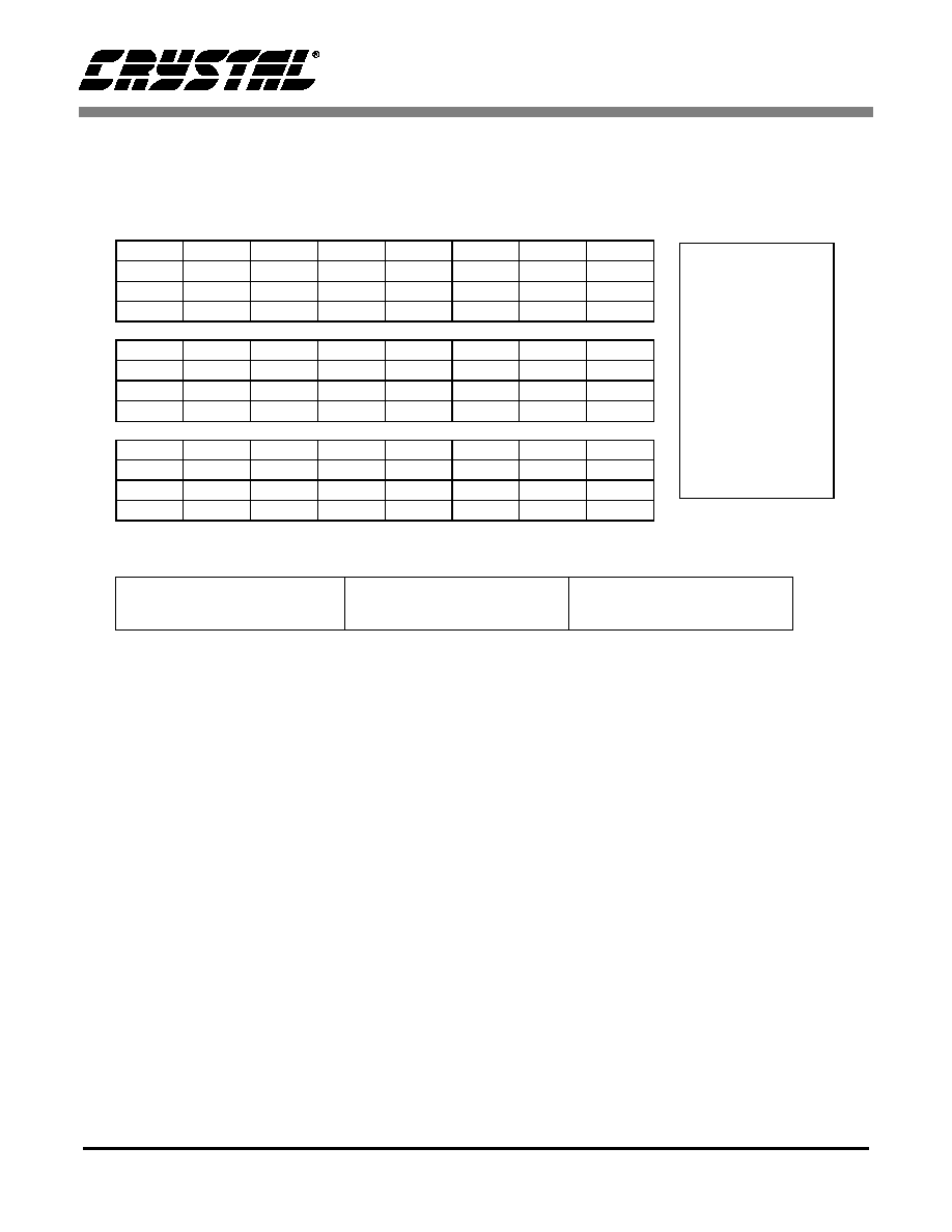
CS5376
DS256PP1
31
5.3.5
SPI1DAT2 Register
(MSB) 23
22
21
20
19
18
17
16
S1DAT23
S1DAT22
S1DAT21
S1DAT20
S1DAT19
S1DAT18
S1DAT17
S1DAT16
R/W
R/W
R/W
R/W
R/W
R/W
R/W
R/W
0
0
0
0
0
0
0
0
15
14
13
12
11
10
9
8
S1DAT15
S1DAT14
S1DAT13
S1DAT12
S1DAT11
S1DAT10
S1DAT9
S1DAT8
R/W
R/W
R/W
R/W
R/W
R/W
R/W
R/W
0
0
0
0
0
0
0
0
7
6
5
4
3
2
1
(LSB) 0
S1DAT7
S1DAT6
S1DAT5
S1DAT4
S1DAT3
S1DAT2
S1DAT1
S1DAT0
R/W
R/W
R/W
R/W
R/W
R/W
R/W
R/W
0
0
0
0
0
0
0
0
SPI 1 Address: 0x09
0x0A
0x0B
--
Not defined;
read as 0
R
Readable
W
Writable
R/W
Readable and
Writable
Bits in bottom rows
are reset condition
Figure 18. SPI 1 Data Register SPI1DAT2
Bit definitions:
23:16 S1DAT[23:16] SPI 1 Data 2 High
Byte
15:8
S1DAT[15:8] SPI 1 Data 2 Middle
Byte
15:8
S1DAT[7:0]
SPI 1 Data 2 Low
Byte

CS5376
DS256PP1
32
5.3.6 SPI 1 Transactions
To send an SPI 1 command to the decimation en-
gine, a microcontroller or other SPI bus master ini-
tiates a serial transaction to write the SPI1CMD,
SPI1DAT1, and SPI1DAT2 registers. Depending
on the command type, additional serial transactions
may be required to write or read data in the
SPI1DAT1 and SPI1DAT2 registers.
At the end of each serial write transaction the SPI 1
port automatically transfers the command and data
values to the decimation engine by setting the
e2dreq bit (external-to-decimation-request bit) in
the SPI1CTRL register. When the written values
are received by the decimation engine, the e2dreq
bit in the SPI1CTRL register is cleared, indicating
that new data can be written.
After writing to the SPI 1 port, the microcontroller
must not overwrite the register values before they
are read by the decimation engine. To ensure this,
the microcontroller should poll the e2dreq bit by
reading the middle byte of the SPI1CTRL register
(SPI1CTRLM) to check if the decimation engine
has received the current data. Alternately, the mi-
crocontroller can delay 1 ms between transactions
to guarantee enough time for the decimation engine
to receive the data.
Command Transactions
All SPI 1 commands require a serial transaction to
write the initial command and data values to the
decimation engine. Depending on the command
type, a single command transaction may be the
only one required.
To send a serial command transaction, the SSI sig-
nal is pulled low and the SPI1CMD, SPI1DAT1,
and SPI1DAT2 registers are written using the
SCK1 and MOSI pins. The full serial transaction
sends the SPI `write' opcode (0x02), the starting
register address (SPI1CMDH 0x03), and up to nine
data bytes. The nine data bytes are the SPI 1 com-
mand code to the SPI1CMD register and the initial
data values to the SPI1DAT1 and SPI1DAT2 reg-
isters. When completed, the SSI signal is pulled
high and the SPI 1 port automatically sets the
e2dreq bit in the SPI1CTRL register to send the
command and data values to the decimation engine.
The decimation engine then uses the SPI1CMD,
SPI1DAT1, and SPI1DAT2 values to start the re-
quested command. After the decimation engine re-
ceives the command and data values, it
automatically clears the e2dreq bit in the
SPI1CTRL register to indicate the SPI 1 port is
available for the next transaction. See "SPI 1 Com-
mands" on page 36 for more information on the
data required for SPI 1 command transactions.
Burst Transactions
Depending on the SPI 1 command, additional
transactions may be required after the initial com-
mand transaction. An SPI 1 burst transaction reads
or writes the SPI1DAT1 and SPI1DAT2 registers
as required by the particular command.
The Read Register command (0x02) reads a data
value from the SPI1DAT1 register using a burst
transaction. All other burst transaction commands,
Write FIR Coefficients (0x03), Write IIR Coeffi-
cients (0x04), and Write TBS Data (0x06) write ad-
ditional data to the decimation engine through the
SPI1DAT1 and SPI1DAT2 registers. See "SPI 1
Commands" on page 36 for more information
about the data required for SPI 1 burst transactions.
To start a serial burst read transaction, the SSI sig-
nal is pulled low and the SPI1DAT1 register is read
using the SCK1, MOSI, and MISO pins. The full
serial transaction sends the SPI `read' opcode
(0x03) with the starting register address
(SPI1DAT1H 0x06) using the SCK1 and MOSI
pins, and receives three data bytes using the SCK1
and MISO pins. The three data bytes returned are
the data value from the SPI1DAT1 register. When
completed, the SSI signal is pulled high to end the
transaction. The e2dreq bit is not used for a read

CS5376
DS256PP1
33
SCK1
MOSI
Figure 19. SPI Slave Mode Transactions
SSI
MSB
LSB
MISO
X
6
1
2
3
4
5
MSB
LSB
6
1
2
3
4
5
1
8
2
7
6
5
4
3
Cycle
MOSI
0x02
ADDR
Data3
MISO
MOSI
MISO
Microcontroller Write to SPI 1
Microcontroller Read from SPI 1
DataN
Data4
SSI
SSI
0x03
ADDR
Data3
DataN
Data4
Instruction
Opcode
Address
Definition
Write
0x02
SPIADDR[7:0]
Write SPI 1 registers beginning at the address
given in SPIADDR. Increment the address for every
byte written.
Read
0x03
SPIADDR[7:0]
Read SPI 1 registers beginning at the address
given in SPIADDR. Increment the address for every
byte read.

CS5376
DS256PP1
34
transaction, a new serial command transaction can
begin immediately.
To send a serial burst write transaction, the SSI sig-
nal is pulled low and the SPI1DAT1 and
SPI1DAT2 registers are written using the SCK1
and MOSI pins. The full serial transaction sends
the SPI `write' opcode (0x02), the starting register
address (SPI1DAT1H 0x06), and up to six data
bytes. The six data bytes write the additional data
values to the SPI1DAT1 and SPI1DAT2 registers.
When completed, the SSI signal is pulled high and
the SPI 1 port automatically sets the e2dreq bit in
the SPI1CTRL register to send the data values to
the decimation engine.
The decimation engine then uses the SPI1DAT1,
and SPI1DAT2 values to service the current com-
mand. After the decimation engine receives the ad-
ditional data values, it automatically clears the
e2dreq bit in the SPI1CTRL register to indicate the
SPI 1 port is available for the next transaction.
Sending SPI 1 commands to the decimation engine:
1) Initiate a serial command transaction to the SPI1CMD, SPI1DAT1, and SPI1DAT2 registers
to write the SPI 1 command and data values.
A serial command transaction uses the SCK1 and MOSI pins to write the SPI `write' opcode
(0x02), the address of the SPI1CMDH register (0x03), and up to nine data bytes.
2) Delay until the command is received by the decimation engine by polling the SPI1CTRLM
register to check if the e2dreq bit is cleared, or by waiting a fixed delay of 1 ms.
The e2dreq bit is checked using the SCK1, MOSI, and MISO pins by writing the SPI `read'
opcode (0x03) and the address of the SPI1CTRLM register (0x01) with the SCK1 and MOSI
pins, and then reading 1 byte of returned data with the SCK1 and MISO pins. The e2dreq bit
is bit 0 of the SPI1CTRLM register (bit 8 of the full SPI1CTRL register).
3) Initiate serial burst transactions, if required by the SPI 1 command, to the SPI1DAT1 and
SPI1DAT2 registers.
A serial burst write transaction uses the SCK1 and MOSI pins to write the SPI `write' opcode
(0x02), the address of the SPI1DAT1H register (0x06), and up to six data bytes.
A serial burst read transaction uses the SCK1, MOSI, and MISO pins by writing the SPI
`read' opcode (0x03) and the address of the SPI1DAT1H register (0x06) with the SCK1 and
MOSI pins, and then reading up to six bytes of returned data with the SCK1 and MISO pins.
4) For serial burst write transactions, delay until the data is received by the decimation engine
by polling the SPI1CTRLM register to check if the e2dreq bit is cleared, or by waiting a fixed
delay of 1ms.
Serial burst read transactions do not require a delay after the data read.

CS5376
DS256PP1
35
E2DREQ Poll Transactions
All SPI 1 command and burst write transactions au-
tomatically use the e2dreq bit in the SPI1CTRL
register to transfer data to the decimation engine.
When the decimation engine clears the e2dreq bit,
the data values were received and another transac-
tion can begin. To ensure the e2dreq bit is cleared
before starting the next transaction, the microcon-
troller can either use single byte read transactions
from the SPI1CTRLM register or can wait a fixed
delay of 1 ms.
To start an e2dreq poll transaction, the SSI signal is
pulled low and the middle byte of the SPI1CTRL
register is read using the SCK1, MOSI, and MISO
pins. The full serial transaction sends the SPI `read'
opcode (0x03) with the starting register address
(SPI1CTRLM 0x01) using the SCK1 and MOSI
pins, and receives one data byte using the SCK1
and MISO pins. The returned data byte is the
SPI1CTRLM register value with bit 0 containing
the e2dreq bit (bit 8 of the full SPI1CTRL register).
When completed, the SSI signal is pulled high to
end the transaction.
After reading the e2dreq bit status, the microcon-
troller checks verify it is cleared. If the e2dreq bit is
0, the decimation engine has received the previous
data and is ready for the next transaction. If the
e2dreq bit is 1, the decimation engine has not re-
ceived the previous data and the next transaction
must be delayed. The microcontroller can wait in a
loop between SPI 1 transactions, continuously
reading the e2dreq bit until it is cleared by the dec-
imation engine.
Alternately, the microcontroller can use a fixed de-
lay of 1 ms between transactions to guarantee the
decimation engine received the previous data. A
fixed delay is useful when initialization timing is
not critical, and only adds a nominal setup time for
most systems.

CS5376
DS256PP1
36
5.3.7 SPI 1 Commands
The SPI 1 commands are used to write and read the
decimation engine registers, write digital filter co-
efficients, write test bit stream generator data, and
enable or disable the digital filters. All configura-
tion of the decimation engine in coprocessor mode
is performed using these commands. Available
SPI 1 to decimation engine commands and their re-
quired register values are listed in Figure 20.
SPI 1 Command
SPI1CMD
SPI1DAT1
1
SPI1DAT2
1
Nop
0x00
--
--
Write Register
0x01
Address
Write Data
Read Register
0x02
Address
[Read Data]
--
--
Write FIR Coefficients
0x03
Num FIR1 Coeff
(FIR Coeff)
Num FIR2 Coeff
(FIR Coeff)
Write IIR Coefficients
0x04
a11
(b11)(a22)(b21)
b10
(a21)(b20)(b22)
Write ROM Coefficients
0x05
--
--
Write TBS Data
0x06
Num TBS Data
(TBS Data)
--
(TBS Data)
Write TBS ROM
0x07
--
--
Filter Start
0x08
--
--
Filter Stop
0x09
--
--
Figure 20. SPI 1 Command Reference
1
(data) indicates multiple data words of this type to be written.
[data] indicates data word to be read from SPI1DAT1 register.
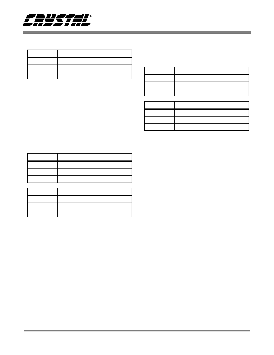
CS5376
DS256PP1
37
Write Register - 0x01
This SPI 1 command writes a data value to a deci-
mation engine register. The decimation engine reg-
ister specified in SPI1DAT1 is written with the data
value in SPI1DAT2.
The CS5376 decimation engine registers control
hardware and filtering functions. See "Register
Summary" on page 94 for information about the bit
definitions of the decimation engine registers.
Read Register - 0x02
This SPI 1 command reads a data value from a dec-
imation engine register. The value of the decima-
tion engine register specified in SPI1DAT1 is
returned in the SPI1DAT1 register. SPI1DAT2 is
not used by this command.
The CS5376 decimation engine registers control
hardware and filtering functions. See "Register
Summary" on page 94 for information about the bit
definitions of the decimation engine registers.
Write FIR Coefficients - 0x03
This SPI 1 command uploads custom coefficients
for the FIR1 and FIR2 filters. A maximum of 255
coefficients can be written for each FIR filter,
though the available decimation engine computa-
tion cycles will limit their practical size. See "Dig-
ital Decimation Filter" on page 53 for more
information about the FIR filters and the cycle lim-
itations of the decimation engine.
The initial SPI command sets the number of FIR1
and FIR2 coefficients to be written. After the initial
write, coefficients for FIR1 and FIR2 are concate-
nated and written to SPI1DAT1 and SPI1DAT2 us-
ing burst transactions. It's not necessary to write
the SPI1CMD register during burst transactions,
but doing so does not affect operation.
During burst writes, the e2dreq bit in the
SPI1CTRL register indicates when to write new
coefficient values. Immediately after data is writ-
ten, the e2dreq bit is automatically set high. When
e2dreq goes low, the data was accepted and new
data can be written.
Register
Command Transaction
SPI1CMD
0x01 - Register Write Command
SPI1DAT1
Register Address
SPI1DAT2
Register Write Data
Register
Command Transaction
SPI1CMD
0x02 - Register Read Command
SPI1DAT1
Register Address
SPI1DAT2
--
Register
Burst Transaction
SPI1CMD
--
SPI1DAT1
[Register Data]
SPI1DAT2
--
Register
Command Transaction
SPI1CMD
0x03 - FIR Coefficient Write Cmd
SPI1DAT1
Number of FIR1 Coefficients
SPI1DAT2
Number of FIR2 Coefficients
Register
Burst Transaction
SPI1CMD
{0x03 - FIR Coefficient Write Cmd}
SPI1DAT1
(FIR Coefficient)
SPI1DAT2
(FIR Coefficient)
CS5376
DS256PP1
38
Write IIR Coefficients - 0x04
This SPI 1 command uploads custom coefficients
for the two stage IIR filter. The IIR filter consists of
a 1st order IIR stage requiring 3 coefficients (a11,
b10, b11) and a 2nd order IIR stage requiring 5 co-
efficients (a21, a22, b20, b21, b22). A 3rd order IIR
filter is implemented by running both stages. See
"Digital Decimation Filter" on page 53 for more in-
formation about the IIR filters.
The required number of IIR coefficients is fixed, so
the initial SPI command writes the first two coeffi-
cients; (a11, b10). After the initial write, the re-
maining IIR coefficients are written to SPI1DAT1
and SPI1DAT2 using burst transactions; (b11,
a21); (a22, b20); (b21, b22). It's not necessary to
write the SPI1CMD register during burst transac-
tions, but doing so does not affect operation.
During burst writes, the e2dreq bit in the
SPI1CTRL register indicates when to write new
coefficient values. Immediately after data is writ-
ten, the e2dreq bit is automatically set high. When
e2dreq goes low, the data was accepted and new
data can be written.
Write ROM Coefficients - 0x05
This SPI 1 command initializes the included coef-
ficients for FIR1, FIR2, and the two stage IIR for
use by the decimation engine. This command only
requires writing the SPI1CMD register; the
SPI1DAT1 and SPI1DAT2 registers are not used.
Write TBS Data - 0x06
This SPI 1 command uploads a custom data set for
the test bit stream generator. This command, along
with the ability to program the TBS generator inter-
polation and clock rate, allows the creation of cus-
tom frequency test signals by the test bit stream
generator. See "Test Bit Stream Generator" on
page 81 for more information on generating specif-
ic test frequencies using custom test bit stream data
sets.
The initial SPI command sets the number of TBS
data to be written. After the initial write, TBS data
values are written to SPI1DAT1 and SPI1DAT2
using burst transactions. It's not necessary to write
the SPI1CMD register during burst transactions,
but doing so does not affect operation.
During burst writes, the e2dreq bit in the SPICTRL
register indicates when to write new coefficient
values. Immediately after data is written, the
Register
Command Transaction
SPI1CMD
0x04 - IIR Coefficient Write Cmd
SPI1DAT1
IIR Coefficient a11
SPI1DAT2
IIR Coefficient b10
Register
Burst Transaction
SPI1CMD
{0x04 - IIR Coefficient Write Cmd}
SPI1DAT1
(IIR Coefficients b11; a22; b21)
SPI1DAT2
(IIR Coefficients a21; b20; b22)
Register
Command Transaction
SPI1CMD
0x05 - ROM Coefficient Write Cmd
SPI1DAT1
--
SPI1DAT2
--
Register
Command Transaction
SPI1CMD
0x06 - TBS Data Write Cmd
SPI1DAT1
Number of TBS Data
SPI1DAT2
--
Register
Burst Transaction
SPI1CMD
{0x06 - TBS Data Write Cmd}
SPI1DAT1
(TBS Data)
SPI1DAT2
(TBS Data)

CS5376
DS256PP1
39
e2dreq bit is automatically set high. When e2dreq
goes low, the data was accepted and new data can
be written.
Write TBS ROM Data - 0x07
This SPI 1 command initializes the included test bit
stream data for use by the test bit stream generator.
This command only requires writing the SPI1CMD
register; the SPI1DAT1 and SPI1DAT2 registers
are not used. See "Test Bit Stream Generator" on
page 81 for more information on generating test
signals using the ROM based test bit stream data
set.
Filter Start - 0x08
This SPI 1 command initializes the decimation en-
gine and starts the digital filters. This command
only requires writing the SPI1CMD register; the
SPI1DAT1 and SPI1DAT2 registers are not used.
The decimation engine will use the filtering config-
uration specified in the FILT_CFG register (0x20)
and coefficients specified by previous SPI 1 com-
mands. See "Digital Decimation Filter" on page 53
for details on decimation engine configurations.
Filter Stop - 0x09
This SPI 1 command disables the digital filters in
the decimation engine. This command only re-
quires writing the SPI1CMD register; the
SPI1DAT1 and SPI1DAT2 registers are not used.
The digital filters are disabled by halting the sinc
filters, which stops the data flow through the digital
filter chain. To place the CS5376 into a low power
standby mode, the decimation engine clock can be
set to 32kHz in the CONFIG register (0x00) after
calling this SPI command.
Register
Command Transaction
SPI1CMD
0x07 - TBS ROM Data Write Cmd
SPI1DAT1
--
SPI1DAT2
--
Register
Command Transaction
SPI1CMD
0x08 - Filter Start Command
SPI1DAT1
--
SPI1DAT2
--
Register
Command Transaction
SPI1CMD
0x09 - Filter Stop Command
SPI1DAT1
--
SPI1DAT2
--

CS5376
DS256PP1
40
6. SERIAL PERIPHERAL INTERFACE 2
The Serial Peripheral Interface 2 (SPI 2) port is a
master-only SPI port designed to simplify the inter-
face to multiple serial peripherals. A microcontrol-
ler or other SPI bus master need only interface with
the CS5376 SPI 1 port to control up to 20 read-only
or 5 read-write serial slave devices using the SPI 2
port. A system block diagram of the SPI 2 port ap-
pears in Figure 21.
6.1 SPI 2 Pin Descriptions
The SPI 2 port uses a common serial clock (SCK2)
and serial output pin (SO), four serial input pins
(SI1 - SI4), and five chip selects (CS0 - CS4) to
communicate with serial peripherals.
SCK2 - Pin 31
Output clock from the Serial Peripheral Interface 2
port. Maximum rate is 4.096 MHz.
SO - Pin 30
Serial Peripheral Interface 2 data output.
SI1 - SI4 - Pins 26 - 29
Serial Peripheral Interface 2 data inputs.
CS0 - CS4 - Pins 32 - 36
Serial Peripheral Interface 2 chip selects.
6.2 SPI 2 Physical Interface
Because SPI 2 slave devices share a common serial
output pin, the exact number that can be controlled
depends on the number of read-write serial devices
connected. Each read-write serial device must con-
nect to a dedicated chip select pin to ensure write
transactions are not received in error by other serial
devices. The remaining chip select pins can be used
for multiple read-only devices, since separate serial
input pins are available for each.
A chip select pin used for read-only serial devices
can select up to four devices, one for every serial
input pin. A serial transaction to a group of read-
only devices selects all using the common chip-se-
lect pin, and they all receive the read request. Each
Figure 21. Serial Peripheral Interface 2 (SPI 2)
SCK2
SI4
SO
CS1
CS2
CS3
CS4
Pin logic
Select
To
G
P
I
O
B
l
o
c
k
Control logic
SPI DACK
SPI DREQ
Data Bus
Interface
8-bit shift register
SPI IRQ
SI2
SI1
SI3
logic
RCH[1:0]
2
4:1
CS0
Decimation
Engine

CS5376
DS256PP1
41
device outputs data based on the read request, and
the CS5376 selects a serial input pin from which to
receive.
As an example, if two read-write serial devices are
to be connected to the SPI 2 port, two chip select
pins must be dedicated to them. The remaining
three chip select pins can each connect up to four
read-only serial devices, for a maximum of two
read-write and twelve read-only devices controlla-
ble through the SPI 2 port.
6.3 SPI 2 Registers
SPI 2 transactions are initiated by writing com-
mand, address, and data values to the SPI2CMD
and SPI2DAT registers, and then writing the
SPI2CTRL register with the D2SREQ bit set. Writ-
ing the D2SREQ bit initiates a transaction using the
programmed configuration.
6.3.1
SPI 2 Command Register
The SPI2CMD register (0x11) is a 16-bit register in
the decimation engine with the high byte designat-
ed as an SPI command and the low byte designated
as an address. The high byte (bits 15-8) holds the
SPI `write' (0x02) or `read' (0x03) command, and
the low byte (bits 7-0) holds an 8-bit destination or
source address.
During a transaction the bytes in SPI2CMD are al-
ways output first, with the SPI2DAT register writ-
ten or read following.
6.3.2
SPI 2 Data Register
The SPI2DAT register (0x12) is a 24-bit register in
the decimation engine with three bytes designated
for serial data. Data in SPI2DAT is always LSB
aligned, with 1-byte data written or received using
the low byte (bits 7-0), 2-byte data written or re-
ceived using the middle and low bytes (bits 15-0),
and 3-byte data written or received using all three
bytes (bits 23-0).
Figure 22. Serial Peripheral Interface 2 Pins
SCK2 - SPI 2 Clock Output, pin 31
Output clock from the Serial Peripheral Interface 2 port. Maximum rate is 4.096 MHz.
SO - SPI 2 Data Output, pin 30
Serial Peripheral Interface 2 data output.
SI1 - SPI 2 Data Input 1, pin 29
Serial Peripheral Interface 2 data input 1.
SI2 - SPI 2 Data Input 2, pin 28
Serial Peripheral Interface 2 data input 2.
SI3 - SPI 2 Data Input 3, pin 27
Serial Peripheral Interface 2 data input 3.
SI4 - SPI 2 Data Input 4, pin 26
Serial Peripheral Interface 2 data input 4.

CS5376
DS256PP1
42
During a transaction the data in the SPI2DAT reg-
ister is written or read after the command and ad-
dress bytes from the SPI2CMD register are written.
6.3.3
SPI 2 Configuration Register
The SPI 2 port is configured using the SPI2CTRL
register (0x10) in the decimation engine. Bits in
this register select the serial input pin and chip se-
lect pin used for a transaction, set the total number
of bytes in a transaction, initiate a transaction using
the D2SREQ bit, and report status and error infor-
mation about a transaction. Other bits in the
SPI2CTRL register set general port configuration
options such as the serial clock rate, the SPI mode,
and the state of the internal pull-up resistors.
Serial Input Configuration
The serial input pin used to receive data is selected
using the SPI2EN bits (bits 19 - 16) and the RCH
bits (bits 14, 15). The SPI2EN bits enable the in-
puts, while the RCH bits select the specific channel
for the SPI 2 transaction.
Chip Select Configuration
The chip select pin used during a transaction is se-
lected using the CS0, CS1, CS2, CS3, and CS4 bits
(bits 0 - 4). Multiple chip selects can be enabled to
send a transaction to more than one serial peripher-
al, if required.
Number of Transaction Bytes
The DNUM bits (bits 5 - 7) are used to specify the
total number of bytes to be transferred during a
transaction. DNUM is zero based and represents
one greater than the number programmed, i.e.
DNUM = 3 specifies a 4 byte transaction.
Initiating SPI 2 Transactions
Writing to the D2SREQ bit (bit 8) starts an SPI 2
transaction. When the transaction is completed, the
D2SREQ bit is automatically cleared.
Status and Error Information
Three bits in the SPI2CTRL register are used to re-
port status and error information.
The D2SOP flag is set when the SPI 2 port is busy
performing a transaction. It is automatically
cleared when the transaction is completed.
The SWEF flag is set if a request to initiate a new
transaction occurs during the current transaction.
This flag is latched and must be cleared manually.
The TM flag indicates the SPI 2 port timed out on
the requested transaction. This flag is latched and
must be cleared manually.
Serial Clock Rate
The output serial clock rate on the SCK2 pin is set
by the SCKFS bits (bits 20 - 22). The clock rate can
be set between 32 kHz and 4.096 MHz.
SPI Mode
The serial mode used for a transaction depends on
the SCKPO and SCKPH bits (bits 10 and 12 re-
spectively). The SPI 2 port supports all SPI modes,
with mode 0 and mode 3 the most commonly used.
SPI Mode 0 (0,0) uses SCKPO = 0 and SCKPH =
0, with SPI mode 3 (1,1) using SCKPO = 1 and
SCKPH = 1.
Internal Pull-Up Resistors
The SPI 2 pins have internal pull-up resistors that
are disabled by setting the WOM bit (bit 23). The
WOM bit enables `wired-or' mode which permits
multiple serial devices to connect together without
the extra power drain of an internal pull-up resistor.
CS5376
DS256PP1
43
6.3.4
SPI2CTRL Register
(MSB) 23
22
21
20
19
18
17
16
WOM
SCKFS2
SCKFS1
SCKFS0
SPI2EN4
SPI2EN3
SPI2EN2
SPI2EN1
R/W
R/W
R/W
R/W
R/W
R/W
R/W
R/W
0
0
1
1
0
0
0
0
15
14
13
12
11
10
9
8
RCH1
RCH0
D2SOP
SCKPH
SWEF
SCKPO
TM
D2SREQ
R/W
R/W
R
R/W
R/W
R/W
R/W
R/W
0
0
0
0
0
0
0
0
7
6
5
4
3
2
1
(LSB) 0
DNUM2
DNUM1
DNUM0
CS4
CS3
CS2
CS1
CS0
R/W
R/W
R/W
R/W
R/W
R/W
R/W
R/W
1
1
1
0
0
0
0
0
I/O Address: 0x10
--
Not defined;
read as 0
R
Readable
W
Writable
R/W
Readable
and Writable
Bits in bottom rows
are reset condition.
Bit definitions:
23
WOM
Wired-OR Mode
1: Enabled (open drain)
0: Disabled (push-pull)
15:14 RCH
[1:0]
SPI2 Read Channel
11: Channel 4
10: Channel 3
01: Channel 2
00: Channel 1
7:5
DNUM
[2:0]
Decimation Engine
Number of bytes in
transaction (1-8)
22:20 SCKFS
[2:0]
SCK2 Frequency
111: reserved
110: reserved
101: 4.096 MHz
100: 2.048 MHz
011: 1.024 MHz
010: 512 kHz
001: 128 kHz
000: 32 kHz
13
D2SOP
DE to SPI2 Operation in
Progress
4
CS4
Chip Select 4 Enable
12
SCKPH
SCK2 Phase
1: Data out at first SCK2
edge
0: Data out before first
SCK2 edge
3
CS3
Chip Select 3 Enable
2
CS2
Chip Select 2 Enable
11
SWEF
SPI2 Write Collision
Error Flag
1
CS1
Chip Select 1 Enable
19:16 SPI2EN
[4:1]
SPI2 Channel Enable
1: Enabled
0: Disabled (default)
10
SCKPO
SCK2 Polarity
1: On falling edge
0: On rising edge
0
CS0
Chip Select 0 Enable
9
TM
SPI2 Timeout
1: SPI2 timed out
0: not timed out
8
D2SREQ DE to SPI2 Request
1: Request operation
0: Operation done
(cleared by SPI2)
Figure 23. SPI 2 Configuration Register SPI2CTRL

CS5376
DS256PP1
44
6.3.5
SPI2CMD Register
(MSB) 23
22
21
20
19
18
17
16
--
--
--
--
--
--
--
--
R/W
R/W
R/W
R/W
R/W
R/W
R/W
R/W
0
0
0
0
0
0
0
0
15
14
13
12
11
10
9
8
SCMD15
SCMD14
SCMD13
SCMD12
SCMD11
SCMD10
SCMD9
SCMD8
R/W
R/W
R/W
R/W
R/W
R/W
R/W
R/W
0
0
0
0
0
0
0
0
7
6
5
4
3
2
1
(LSB) 0
SCMD7
SCMD6
SCMD5
SCMD4
SCMD3
SCMD2
SCMD1
SCMD0
R/W
R/W
R/W
R/W
R/W
R/W
R/W
R/W
0
0
0
0
0
0
0
0
I/O Address: 0x11
--
Not defined;
read as 0
R
Readable
W
Writable
R/W
Readable and
Writable
Bits in bottom rows
are reset condition
Bit definitions:
23:16 --
reserved
15:8
SCMD[15:8] SPI2 Upper Command
Byte
15:8
SCMD[7:0]
SPI2 Lower Command
Byte
Figure 24. SPI 2 Command Register SPI2CMD

CS5376
DS256PP1
45
6.3.6
SPI2DAT Register
(MSB) 23
22
21
20
19
18
17
16
SDAT23
SDAT22
SDAT21
SDAT20
SDAT19
SDAT18
SDAT17
SDAT16
R/W
R/W
R/W
R/W
R/W
R/W
R/W
R/W
0
0
0
0
0
0
0
0
15
14
13
12
11
10
9
8
SDAT15
SDAT14
SDAT13
SDAT12
SDAT11
SDAT10
SDAT9
SDAT8
R/W
R/W
R/W
R/W
R/W
R/W
R/W
R/W
0
0
0
0
0
0
0
0
7
6
5
4
3
2
1
(LSB) 0
SDAT7
SDAT6
SDAT5
SDAT4
SDAT3
SDAT2
SDAT1
SDAT0
R/W
R/W
R/W
R/W
R/W
R/W
R/W
R/W
0
0
0
0
0
0
0
0
I/O Address: 0x12
--
Not defined;
read as 0
R
Readable
W
Writable
R/W
Readable and
Writable
Bits in bottom rows
are reset condition
Figure 25. SPI 2 Data Register SPI2DAT
Bit definitions:
23:16 SDAT[23:16]
SPI2 Upper Data
Byte
15:8
SDAT[15:8]
SPI2 Middle Data
Byte
15:8
SDAT[7:0]
SPI2 Lower Data
Byte

CS5376
DS256PP1
46
6.4
SPI 2 Transactions
The SPI 2 port operates as an SPI master to perform
write and read transactions with serial slave periph-
erals. The exact timing of the SPI transactions de-
pends on the SPI mode, selected using the SCKPO
and SCKPH bits in the SPI2CTRL register.
Write Transactions
Write transactions are initialized by writing an SPI
`write' (0x02) opcode and an 8-bit destination ad-
dress to the SPI2CMD register, and the output data
value to the SPI2DAT register. Writing the
D2SREQ bit in the SPI2CTRL register starts the
SPI 2 transaction based on the SPI2CTRL configu-
ration.
A write transaction outputs 1 or 2 bytes from the
SPI2CMD register and 0, 1, 2, or 3 bytes from the
SPI2DAT register. Write transactions are therefore
a minimum of 1 byte (DNUM = 0) and a maximum
of 5 bytes (DNUM = 4). The SPI 2 port uses the
DNUM bits in the SPI2CTRL register to determine
the total number of bytes to send during a write
transaction.
Write transactions are not required to use standard
SPI commands. If serial peripherals use non-stan-
dard write commands they can be written to the
SPI2CMD and SPI2DAT registers as required.
Read Transactions
Read transactions are initialized by writing an SPI
`read' (0x03) opcode and an 8-bit source address to
the SPI2CMD register. Writing the D2SREQ bit in
the SPI2CTRL register starts the SPI 2 transaction
based on the SPI2CTRL configuration, with the in-
put data value received to the SPI2DAT register.
A read transaction outputs 2 bytes from the
SPI2CMD register and can receive 1, 2, or 3 bytes
into the SPI2DAT register. Read transactions are a
minimum of 3 bytes (DNUM = 2) and a maximum
of 5 bytes (DNUM = 4). The SPI 2 port uses the
DNUM bits in the SPI2CTRL register to determine
the total number of bytes to send and receive during
a read transaction.
Read transactions are not required to use standard
SPI commands. If a serial peripherals use non-stan-
dard read commands they can be written to the
SPI2CMD register, as long as they conform to the
format of 2 bytes out with 1, 2, or 3 bytes in.
SPI Modes
The SPI mode for the SPI 2 port is selected in the
SPI2CTRL register using the SCKPO and SCKPH
bits. Supported modes are:
SPI Mode 0 (0,0): SCKPO = 0, SCKPH = 0
SPI Mode 1 (0,1): SCKPO = 0, SCKPH = 1
SPI Mode 2 (1,0): SCKPO = 1, SCKPH = 0
SPI Mode 3 (1,1): SCKPO = 1, SCKPH = 1
The most commonly used SPI modes are mode 0
and mode 3, both of which define the serial clock
with data valid on rising edges and transitioning on
falling edges.
In SPI mode 0, the SCK2 serial clock is defined ini-
tially in a low state. Output data on the SO pin is
valid immediately after the chip select pin goes
low, and the first rising edge of SCK2 latches valid
data.
In SPI mode 3, the SCK2 serial clock is defined ini-
tially in a high state. Output data on the SO pin is
invalid until the initial falling edge of SCK2, and
the first rising edge of SCK2 latches valid data.
SPI modes 1 and 4 work similarly to modes 0 and
3, with the serial clock defined to have data valid on
falling edges and transitioning on rising edges.

CS5376
DS256PP1
47
Figure 26. SPI 2 Master Mode Transactions
SO
0x02
ADDR
Data1
SI
SO
SI
SPI 2 Write to External Slave
SPI 2 Read from External Slave
Data3
Data2
0x03
ADDR
Data1
Data3
Data2
CS
CS
SPI2CMD[15:8]
SPI2CMD[7:0]
SPI2DAT
SPI2CMD[15:8]
SPI2CMD[7:0]
SPI2DAT
Instruction
Opcode
Address
Definition
Write
0x02
SPI2CMD[7:0]
Write serial peripheral beginning at the address
given in SPI2CMD[7:0]. Increment the address for
every byte written from SPI2DAT.
Read
0x03
SPI2CMD[7:0]
Read serial peripheral beginning at the address
given in SPI2CMD[7:0]. Increment the address for
every byte read to SPI2DAT.
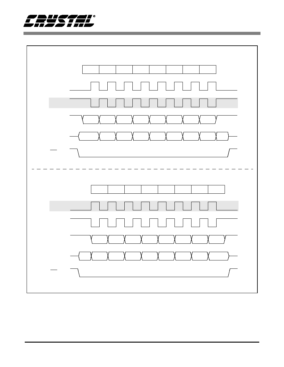
CS5376
DS256PP1
48
SCK2
SO
Figure 27. SPI 2 Transaction Details
CS
MSB
LSB
SCK2
SI
SCKPO = 0
SCKPO = 1
X
6
1
2
3
4
5
LSB
MSB
6
1
2
3
4
5
1
8
2
7
6
5
4
3
Cycle
Slave devices only drive SI after being selected and responding to a read command.
SCK2
SO
CS
MSB
LSB
SCK2
SI
SCKPO = 0
SCKPO = 1
X
6
1
2
3
4
5
MSB
LSB
6
1
2
3
4
5
1
8
2
7
6
5
4
3
Cycle
Slave devices only drive SI after being selected and responding to a read command.
SPI 2 Transaction with SCKPH=0
SPI 2 Transaction with SCKPH=1

CS5376
DS256PP1
49
7. MODULATOR DATA INTERFACE
The CS5376 provides digital filtering for up to four
- modulators. The signals to and from the mod-
ulators are connected through the modulator data
interface (MDI).
7.1 Modulator Interface Pin Descriptions
Each modulator has a dedicated data input to an
MDATA pin, a dedicated error flag input to an
MFLAG pin, a shared modulator clock signal from
the MCLK pin, and a shared synchronization signal
from the MSYNC pin.
MCLK, MCLK/2 - Pins 13, 12
Generated output clocks for the modulators.
MSYNC - Pin 14
Generated output synchronization signal to reini-
tialize the modulator timing. Generated from the
SYNC input signal.
MDATA1 - MDATA4 - Pins 15, 17, 19, 21
Modulator data input, a one-bit serial data stream
(one's density) at a rate dictated by the rate of the
MCLK signal. 512 kbit and 256 kbit are typical
MDATA rates.
MFLAG1 - MFLAG4 - Pins 16, 18, 20, 22
Logic input indicating the modulator is unstable
due to an over-ranged signal on its analog input.
7.2 Modulator Data Inputs
The MDATA inputs are expected to be 1-bit
-
data at a 512 kHz or 256 kHz rate. The
one's den-
sity input is defined as full scale positive at 86%
and full scale negative at 14%, with overhang capa-
bility to 93% and 7%. Note that no signal input pro-
duces a 50% one's density from the modulators.
The CS5372 modulator generates compatible data
at a 512 kHz rate, while the CS5321 modulator
generates compatible data at a 256 kHz rate. Both
data rates use an MDIFS setting of 512 kHz in the
CONFIG register (0x00) since the 256 kHz data
rate can be oversimple.
7.3 Modulator Flag Inputs
An MFLAG signal from a modulator indicates it
has become unstable due to an overrange condition
Figure 28. Modulator Data Interface
FIR
IIR
Filters
Filter
Output to High Speed Serial Data Port (SD Port)
DC Offset
Correction
Output Rate 62.5 Hz ~ 4 kHz
& Gain
MDATA[4:1]
MFLAG[4:1]
MDI Input
512 kHz
MCLK /
Generate
MSYNC
CLK
SYNC
MSYNC
SINC
Filter
MCLK
MCLK/2

CS5376
DS256PP1
50
on the analog inputs. Once the overrange signal is
removed, the modulator recovers and the MFLAG
signal is cleared. The invalid data during the over-
range condition must propagate through the filter
chain, so the digital filters require time to recover
after an MFLAG error.
The MFLAG pin input value is included as an error
flag in the SD port status byte for that channel.
When an MFLAG signal is received from a modu-
lator, the error flag is output in the next status byte
without delay. Depending on the group delay of the
digital filters, a few words of valid data will be out-
put from the SD port before the invalid data propa-
gates through. See "Serial Data Output Port" on
page 71 for more information on the SD port status
byte and the MFLAG error bit.
7.4 Modulator Clock Generation
The MCLK and MCLK/2 outputs are low-jitter,
low-skew modulator clocks. The MCLK pin can
generate a 4.096 MHz, 2.048 MHz, 1.024 MHz, or
512 kHz clock from a 32.768 MHz master clock,
with the rate selected in the CONFIG register
(0x00). MCLK/2 always produces a clock at half
the selected MCLK rate. The CS5372 modulator
expects an MCLK rate of 2.048 MHz, while the
CS5321 expects an MCLK rate of 1.024 MHz.
7.4.1
Modulator Clock Enables
The MCKEN and MCKEN2 bits in the CONFIG
register independently enable the MCLK and
MCLK/2 outputs. At powerup or after RESET, the
MCLK and MCLK/2 pins are disabled and driven
low. When system configuration sets the MCKEN
or MCKEN2 bits, the internally-generated MCLK
Figure 29. Modulator Data Interface Pins
MCLK - Modulator Clock Output, pin 13
Generated output clock to operate the CS5372 modulator. The clock frequency is
selectable, typically 2.048 MHz.
MCLK/2 - Modulator Clock Divided by 2 Output, pin 12
Generated output clock to operate the CS5321 modulator. The clock frequency is
selectable, typically 1.024 MHz.
MSYNC - Modulator Sync Output, pin 14
Generated output synchronization signal to reinitialize the modulator timing. Generated
from the SYNC input signal.
MDATA[4:1] - Modulator Data Input, pin 15, 17, 19, 21
Modulator data input, a one-bit serial data stream (one's density) at a rate dictated by
the rate of the MCLK signal. 512 kbit and 256 kbit are typical MDATA rates.
MFLAG[4:1] - Modulator Flag Input, pin 16, 18, 20, 22
Logic input indicating the modulator is unstable due to an over-ranged signal on its
analog input.

CS5376
DS256PP1
51
or MCLK/2 signals begin driving their respective
pins starting from the next internal 32 kHz clock
synchronization boundary.
7.5 Modulator Synchronization
The MSYNC output is generated from an external
input on the SYNC pin. MSYNC phase aligns the
sampling instant of the modulators and guarantees
synchronous analog sampling across a measure-
ment network. See "System Synchronization" on
page 77 for more information about how the
MSYNC signal is generated from the SYNC input.
7.5.1
Modulator Sync Enable
Clearing the MSEN bit in the CONFIG register
(0x00) disables generation of the MSYNC signal,
the default state is for MSYNC generation to be en-
abled.
MSYNC
MCLK
MDATAx
Figure 30. SYNC and MSYNC Timing
(2.048 MHz)
t
msd
t
msd
(512 kHz)
t
msh
Note: MDATA at 256 kHz has the same start timing, but takes 8 MCLK cycles to update.
Data1
Data2
t
msd
= T
MCLK
/ 4
t
msh
= T
MCLK
For f
MCLK
= 2.048 MHz:
t
msd
= 122 ns
t
msh
= 488 ns
SYNC

CS5376
DS256PP1
52
7.5.2
CONFIG Register
(MSB)23
22
21
20
19
18
17
16
--
--
--
--
--
DFS2
DFS1
DFS0
R/W
R/W
R/W
R/W
R/W
R/W
R/W
R/W
0
0
0
0
0
1
0
1
15
14
13
12
11
10
9
8
--
WDFS2
WDFS1
WDFS0
--
MCKFS2
MCKFS1
MCKFS0
R/W
R/W
R/W
R/W
R/W
R/W
R/W
R/W
0
0
0
0
0
1
0
0
7
6
5
4
3
2
1
(LSB)0
--
--
MCKEN2
MCKEN
MDIFS
SBY
BOOT
MSEN
R/W
R/W
R/W
R/W
R/W
R/W
R
R/W
0
0
0
0
0
0
0
1
Figure 31. Decimation Engine Configuration Register CONFIG
Bit definitions:
23:19 --
reserved
15
--
reserved
7:6
--
reserved
18:16 DFS
[2:0]
Decimation Engine
Frequency Select
111: reserved
110: 8.192 MHz
101: 4.096 MHz
(default)
100: 2.048 MHz
011: 1.024 MHz
010: 512 kHz
001: 256 kHz
000: 32 kHz
14:12 WDFS
[2:0]
Watchdog Frequency
Select
111: reserved
110: 8.192 MHz
101: 4.096 MHz
100: 2.048 MHz
011: 1.024 MHz
010: 512 kHz
001: 256 kHz
000: 32 kHz (default)
5
MCKEN2
MCLK/2 Output Enable
4
MCKEN
MCLK Output Enable
3
MDIFS
MDI Frequency Select:
1: 256 kHz
0: 512 kHz (default)
2
SBY
Standby
1: DE in low power, low
frequency mode
0: DE normal operation
11
--
reserved
10:8
MCKFS
[2:0]
MCLK Frequency Select
111: reserved
110: reserved
101: 4.096 MHz
100: 2.048 MHz
(default)
011: 1.024 MHz
010: 512 kHz
001: reserved
000: reserved
1
BOOT
Boot Source Select
1: Boot from PROM
0: Boot from SPI
0
MSEN
MSYNC Enable
1: MSYNC is generated
from SYNC
0: MSYNC remains low
I/O Address: 0x00
--
Not defined;
read as 0
R
Readable
W
Writable
R/W
Readable and
Writable
Bits in bottom rows
are reset condition

CS5376
DS256PP1
53
8. DIGITAL DECIMATION FILTER
The CS5376 digital filter consists of three sections:
a hardware sinc filter, two FIR filters, and a select-
able 1st, 2nd, or 3rd order IIR filter. The coeffi-
cients for the FIR and IIR filters are programmable
via the SPI 1 serial port, allowing the use of custom
filter sets optimized for specific applications. Ref-
erence coefficients are included in the CS5376
which are suitable for many applications.
Figure 32 illustrates the general flow of the filter
chain, along with the decimation ratios for each fil-
ter stage. The digital filters are structured to allow
data output following any stage in the filter chain.
If an application requires only a single FIR filter,
for example, conversion data can be taken immedi-
ately following the FIR1 filter stage.
The CS5376 digital filter supports output word
rates (OWRs) between 62.5 Hz and 4 kHz, though
not all output rates are supported for all output con-
figurations. The available decimation ratios limit
the FIR1 output configuration to output word rates
between 250 Hz and 4 kHz, while the sinc filter
output configuration supports only a 4 kHz output
word rate.
8.1 Filter Initialization
The CS5376 digital filters are initialized by setting
the decimation engine clock in the CONFIG regis-
ter (0x00), and then setting filter parameters in the
FILT_CFG register (0x20).
8.1.1
Decimation Engine Clock
The FIR and IIR filters are run in the decimation
engine, which is optimized for low-power digital
filter computations. The decimation engine clock
rate is programmable between 8.192 MHz and 32
kHz using the DFS bits (bits 16-18) in the CONFIG
register.
Computation Cycles
The appropriate decimation engine clock rate de-
pends on the computation cycles required to com-
plete the digital filters at the selected output word
rate. Lower clock rates consume less power but
cannot complete complex filters at high output
word rates.
Filter complexity is proportional to the total num-
ber of FIR filter coefficients and the selected order
of the IIR filter. Some experimentation will be re-
Figure 32. Digital Decimation Filter Stages
Sinc Filter
16-128
FIR1
4,16
FIR2
2,4
IIR1
IIR2
1st Order
2nd Order
Output to High Speed Serial Data Port (SD Port)
DC Offset
Correction
Output Rate 62.5 Hz ~ 4 kHz
& Gain
Modulator
512 kHz
Input

CS5376
DS256PP1
54
quired to determine the minimum clock rate that
can support a specified digital filter configuration.
Low-Power Standby Modes
A low-power standby mode exists to force the dec-
imation engine clock to 32 kHz, regardless of the
clock rate setting in the CONFIG register. This
mode is intended for battery powered systems that
idle for extended periods. The SBY bit (bit 2) in the
CONFIG register enables the decimation engine
low-power standby mode.
Standby mode slows the decimation engine clock,
but does not halt filter operation. To place the
CS5376 into a full sleep mode, the `Stop Filter'
command in the SPI 1 port should be issued to dis-
able the digital filters. The `Stop Filter' command
halts the sinc filter and disables writes to the SD
port, placing these blocks into a low-power state.
After the filters are stopped, setting the SBY bit in
the CONFIG register minimizes power in the deci-
mation engine. While writing the SBY bit, clearing
the MCKEN and MCKEN2 bits disables the mod-
ulator clocks and places the modulators into a low-
power state.
To recover from sleep mode, write the CONFIG
register to clear the SBY bit and re-enable the mod-
ulator clocks, and then send the `Start Filter' SPI 1
command. See "Serial Peripheral Interface 1" on
page 21 for a description of the `Stop Filter', `Start
Filter', and register write SPI 1 commands.
8.1.2
Channel Enable
The CS5376 can perform digital filtering for up to
four
- modulators. The number of enabled chan-
nels is set by the CH bits (bits 0,1) in the
FILT_CFG register. The channels are enabled se-
quentially, with the one channel configuration us-
ing channel 1, the two channel configuration using
channels 1 and 2, the three channel configuration
using channels 1, 2, and 3, and the four channel
configuration using all four channels.
When fewer than four channels are required, the
number of decimation engine computation cycles
required to complete the digital filters is reduced
proportionally. This permits slower decimation en-
gine clock rates, and lower power consumption, for
reduced channel count applications.
8.1.3
Output Filter Selection
The CS5376 digital filters can output data follow-
ing any stage in the filter chain. The output filter
stage is selected using the FSEL bits (bits 8-10) in
the FILT_CFG register. Output data can be taken
from the sinc filter, the FIR1 filter, the FIR2 filter,
the 1st order IIR filter, the 2nd order IIR filter, or
the 3rd order IIR filter (by running both the 1st and
2nd order IIR filters).
When an output filter stage is selected, earlier filter
stages must be completed. For example, it is not
possible to run only the 1st order IIR filter without
first running the FIR1 and FIR2 filters. One excep-
tion is the 2nd order IIR filter which automatically
bypasses the 1st order IIR filter.

CS5376
DS256PP1
55
8.1.4
Output Word Rate
The CS5376 digital filters support output word
rates (OWRs) between 62.5 Hz and 4 kHz. The out-
put word rate is selected using the DEC bits (bits 4-
6) in the FILT_CFG register, with the decimation
ratios for each filter stage set automatically de-
pending on the output filter configuration. Figure
33 lists the decimation settings based on the select-
ed output configuration.
Not all output rates are supported for all output fil-
ter configurations. The available decimation ratios
limit the FIR1 output configuration to output word
rates between 250 Hz and 4 kHz, and the sinc filter
output configuration to a single 4 kHz output word
rate. Selecting an unsupported output word rate re-
sults in the closest supported output word rate.
Sinc Filter Output Configuration - FSEL Bits = 0x00
FIR1 Filter Output Configuration - FSEL Bits = 0x01
FIR2 Filter, IIR Filter Output Configurations - FSEL Bits = 0x02, 0x03, 0x04, 0x05
Output
Word Rate
DEC Bits
Setting
Input Bit
Rate
Sinc
Decimation
FIR1
Decimation
FIR2
Decimation
Total
Decimation
4 kHz
0x07
512 kHz
128
-
-
128
Output
Word Rate
DEC Bits
Setting
Input Bit
Rate
Sinc
Decimation
FIR1
Decimation
FIR2
Decimation
Total
Decimation
4 kHz
0x07
512 kHz
32
4
-
128
2 kHz
0x06
512 kHz
64
4
-
256
1 kHz
0x05
512 kHz
128
4
-
512
500 Hz
0x04
512 kHz
64
16
-
1024
333.3 Hz
0x03
512 kHz
96
16
-
1536
250 Hz
0x02
512 kHz
128
16
-
2048
Output
Word Rate
DEC Bits
Setting
Input Bit
Rate
Sinc
Decimation
FIR1
Decimation
FIR2
Decimation
Total
Decimation
4 kHz
0x07
512 kHz
16
4
2
128
2 kHz
0x06
512 kHz
32
4
2
256
1 kHz
0x05
512 kHz
64
4
2
512
500 Hz
0x04
512 kHz
128
4
2
1024
333.3 Hz
0x03
512 kHz
96
4
4
1536
250 Hz
0x02
512 kHz
64
16
2
2048
125 Hz
0x01
512 kHz
128
16
2
4096
62.5 Hz
0x00
512 kHz
128
16
4
8192
Figure 33. Supported Output Word Rates

CS5376
DS256PP1
56
8.1.5
CONFIG Register
(MSB)23
22
21
20
19
18
17
16
--
--
--
--
--
DFS2
DFS1
DFS0
R/W
R/W
R/W
R/W
R/W
R/W
R/W
R/W
0
0
0
0
0
1
0
1
15
14
13
12
11
10
9
8
--
WDFS2
WDFS1
WDFS0
--
MCKFS2
MCKFS1
MCKFS0
R/W
R/W
R/W
R/W
R/W
R/W
R/W
R/W
0
0
0
0
0
1
0
0
7
6
5
4
3
2
1
(LSB)0
--
--
MCKEN2
MCKEN
MDIFS
SBY
BOOT
MSEN
R/W
R/W
R/W
R/W
R/W
R/W
R
R/W
0
0
0
0
0
0
0
1
Figure 34. Decimation Engine Configuration Register CONFIG
Bit definitions:
23:19 --
reserved
15
--
reserved
7:6
--
reserved
18:16 DFS
[2:0]
Decimation Engine
Frequency Select
111: reserved
110: 8.192 MHz
101: 4.096 MHz
(default)
100: 2.048 MHz
011: 1.024 MHz
010: 512 kHz
001: 256 kHz
000: 32 kHz
14:12 WDFS
[2:0]
Watchdog Frequency
Select
111: reserved
110: 8.192 MHz
101: 4.096 MHz
100: 2.048 MHz
011: 1.024 MHz
010: 512 kHz
001: 256 kHz
000: 32 kHz (default)
5
MCKEN2
MCLK/2 Output Enable
4
MCKEN
MCLK Output Enable
3
MDIFS
MDI Frequency Select:
1: 256 kHz
0: 512 kHz (default)
2
SBY
Standby
1: DE in low power, low
frequency mode
0: DE normal operation
11
--
reserved
10:8
MCKFS
[2:0]
MCLK Frequency Select
111: reserved
110: reserved
101: 4.096 MHz
100: 2.048 MHz
(default)
011: 1.024 MHz
010: 512 kHz
001: reserved
000: reserved
1
BOOT
Boot Source Select
1: Boot from PROM
0: Boot from SPI
0
MSEN
MSYNC Enable
1: MSYNC is generated
from SYNC
0: MSYNC remains low
I/O Address: 0x00
--
Not defined;
read as 0
R
Readable
W
Writable
R/W
Readable and
Writable
Bits in bottom rows
are reset condition

CS5376
DS256PP1
57
8.1.6
FILT_CFG Register
(MSB) 23
22
21
20
19
18
17
16
--
--
--
EXP4
EXP3
EXP2
EXP1
EXP0
R/W
R/W
R/W
R/W
R/W
R/W
R/W
R/W
0
0
0
0
0
0
0
0
15
14
13
12
11
10
9
8
--
ORCAL
USEOR
USEGR
--
FSEL2
FSEL1
FSEL0
R/W
R/W
R/W
R/W
R/W
R/W
R/W
R/W
0
0
0
0
0
0
0
0
7
6
5
4
3
2
1
(LSB) 0
--
DEC2
DEC1
DEC0
--
--
CH1
CH0
R/W
R/W
R/W
R/W
R/W
R/W
R/W
R/W
0
0
0
0
0
0
0
0
I/O Address: 0x20
--
Not defined;
read as 0
R
Readable
W
Writable
R/W
Readable and
Writable
Bits in bottom rows
are reset condition
Bit definitions:
23:21 --
reserved
15
--
reserved
7
--
reserved
21:16 EXP[4:0] DC Offset Calibration
Routine Exponent
(Determines sensitivity
of DC offset calibration
routine)
14
ORCAL
Offset Register Calibra-
tion Routine Enable
1: enabled
0: disabled
6:4
DEC[2:0]
Decimation Rate, Output
Word Rate
111: 4 kHz
110: 2 kHz
101: 1 kHz
100: 500 Hz
011: 333.3 Hz
010: 250 Hz
001: 125 Hz
000: 62.5 Hz
13
USEOR
Use Offset Register Cor-
rection
1: enabled
0: disabled
3:2
--
reserved
12
USEGR
[11:8]
Use Gain Register Cor-
rection
1: enabled
0: disabled
1:0
CH[1:0]
Channel Enable
11: 3 Channel (1, 2, 3)
10: 2 Channel (1, 2)
01: 1 Channel (1 only)
00: 4 Channel (1, 2, 3, 4)
11
--
reserved
10:8
FSEL[2:0] Output Filter Select
111: reserved
110: reserved
101: IIR 3rd Order
100: IIR 2nd Order
011: IIR 1st Order
010: FIR2 Output
001: FIR1 Output
000: Sinc Output
Figure 35. Filter Configuration Register FILT_CFG

CS5376
DS256PP1
58
8.2 Hardware Sinc Filter
The hardware sinc filter provides high-order atten-
uation of out-of-band noise components from the
- modulators. It also decimates the 512 kHz 1-
bit
- data into lower frequency 24-bit data suit-
able for the FIR and IIR filters.
The hardware sinc filter is divided into two cascad-
ed sections, Sinc1 and Sinc2. Sinc1 is a fixed 5th
order decimate by 8 sinc filter while Sinc2 is a
multi-stage variable order sinc filter capable of
decimation ratios of 2, 4, 8, 12, or 16. The selected
output word rate and output filter stage from the
overall filter chain automatically determines the
decimation ratio selected for Sinc2.
Once the decimation ratio for Sinc2 is set, all en-
abled channels are decimated and filtered using an
identical hardware algorithm. The final output
from the sinc filter is 24-bit 2's complement data
that passes to the decimation engine for further fil-
tering by the FIR and IIR stages.
8.2.1
SINC1 Filter
The first part of the hardware sinc filter is Sinc1, a
fixed 5th order decimate by 8 sinc filter. This filter
decimates the incoming 512 kHz (or oversampled
256 kHz) 1-bit
- bit stream from the modulators
down to a 64 kHz rate.
This filter section can be modeled as a 5th order
sinc filter with a decimate by 8 output. The time do-
main coefficients are [1, 5, 10, 10, 5, 1], and the fre-
quency domain model is [(sin x)/x]
5
.
8.2.2
SINC2 Filter
The second part of the hardware sinc filter is Sinc2,
a multi-stage, variable order, variable decimation
sinc filter. Depending on the selected output word
rate and output filter stage from the overall filter
chain, different cascaded Sinc2 stages are enabled.
See Figure 37 for a listing of possible Sinc2 config-
urations.
Stage 1 of Sinc2 can be modeled as a 4th order sinc
filter with a decimate by 2 output. The time domain
sinc1
8
sinc2
2
sinc2
2
sinc2
2
sinc2
2
sinc2
3
5th order
5th order
6th order
4th order
4th order
4th order
4 kHz -
Figure 36. Sinc1 and Sinc2 Filter Stages
512 kHz
1-bit
-,
24-bit,
32 kHz
stage1
stage3
stage4
stage5
stage2

CS5376
DS256PP1
59
coefficients are [1, 4, 6, 4, 1], and the frequency do-
main model is [(sin x)/x]
4
.
Stage 2 of Sinc2 can be modeled as a 4th order sinc
filter with a decimate by 3 output. The time domain
coefficients are [1, 4, 6, 4, 1], and the frequency do-
main model is [(sin x)/x]
4
.
Stage 3 of Sinc2 can be modeled as a 4th order sinc
filter with a decimate by 2 output. The time domain
coefficients are [1, 4, 6, 4, 1], and the frequency do-
main model is [(sin x)/x]
4
.
Stage 4 of Sinc2 can be modeled as a 5th order sinc
filter with a decimate by 2 output. The time domain
coefficients are [1, 5, 10, 10, 5, 1], and the frequen-
cy domain model is [(sin x)/x]
5
.
Sinc Filter Output Configuration - FSEL Bits = 0x00
FIR1 Filter Output Configuration - FSEL Bits = 0x01
FIR2 Filter, IIR Filter Output Configurations - FSEL Bits = 0x02, 0x03, 0x04, 0x05
Output
Word Rate
DEC Bits
Setting
Input Bit
Rate
1
Sinc1
Decimation
Sinc2
Decimation
Sinc2
Stages
Sinc
Output
4 kHz
0x07
512 kHz
8
16
1,3,4,5
4 kHz
Output
Word Rate
DEC Bits
Setting
Input Bit
Rate
1
Sinc1
Decimation
Sinc2
Decimation
Sinc2
Stages
Sinc
Output
4 kHz
0x07
512 kHz
8
4
4,5
16 kHz
2 kHz
0x06
512 kHz
8
8
3,4,5
8 kHz
1 kHz
0x05
512 kHz
8
16
1,3,4,5
4 kHz
500 Hz
0x04
512 kHz
8
8
3,4,5
8 kHz
333.3 Hz
0x03
512 kHz
8
12
2,4,5
5.33 kHz
250 Hz
0x02
512 kHz
8
16
1,3,4,5
4 kHz
Output
Word Rate
DEC Bits
Setting
Input Bit
Rate
1
Sinc1
Decimation
Sinc2
Decimation
Sinc2
Stages
Sinc
Output
4 kHz
0x07
512 kHz
8
2
5
32 kHz
2 kHz
0x06
512 kHz
8
4
4,5
16 kHz
1 kHz
0x05
512 kHz
8
8
3,4,5
8 kHz
500 Hz
0x04
512 kHz
8
16
1,3,4,5
4 kHz
333.3 Hz
0x03
512 kHz
8
12
2,4,5
5.33 kHz
250 Hz
0x02
512 kHz
8
8
3,4,5
8 kHz
125 Hz
0x01
512 kHz
8
16
1,3,4,5
4 kHz
62.5 Hz
0x00
512 kHz
8
16
1,3,4,5
4 kHz
Figure 37. Sinc Filter Configurations
1
A 256 kHz input rate is oversampled to match the 512 kHz settings.

CS5376
DS256PP1
60
Stage 5 of Sinc2 can be modeled as a 6th order sinc
filter with a decimate by 2 output. The time domain
coefficients are [1, 6, 15, 20, 15, 6, 1], and the fre-
quency domain model is [(sin x)/x]
6
.
8.2.3
Sinc Filter Synchronization
The sinc filter is synchronized to the external sys-
tem by the MSYNC signal, which is generated
from the SYNC input. The MSYNC signal sets a
reference time (time 0) for all filter operations, and
the sinc filter is restarted to phase align with this
reference time. See "System Synchronization" on
page 77 for information about how the MSYNC
signal is generated.
During synchronization, the sinc filter resets all in-
ternal address pointers and restarts the filter on the
next data input. Existing data in the internal data
registers is not cleared, so immediately after syn-
chronization the data from the sinc filter will be a
combination of pre-sync and post-sync data.
8.3 FIR Filters
The finite impulse response (FIR) filter block con-
sists of two cascaded filters, FIR1 and FIR2, that
can each be programmed with a maximum of 255
coefficients. FIR coefficients in the CS5376 are 24-
bit 2's complement values normalized to
0x7FFFFF (decimal 8388607).
The programmed coefficients for the FIR filters are
completely arbitrary and can implement any type
of finite impulse response filter. Linear phase, min-
imum phase, phase compensation, or other com-
plex filter types can be used depending on the
application requirements. The ability to write and
re-write filter coefficients through the SPI 1 port
also allows quasi-adaptive filters, though updating
coefficients during operation without disrupting
the output data stream is not possible.
8.3.1
FIR1 Filter
The FIR1 filter stage has a decimate by 4 or 16 ar-
chitecture, and can be programmed with a maxi-
mum of 255 coefficients. The coefficients should
be normalized to 24-bit 2's complement full scale,
0x7FFFFF (decimal 8388607).
The characteristic equation for FIR1 is a convolu-
tion of the input values, X(n), and the filter coeffi-
cients, h(k), to produce an output value, Y.
Y = [h(k)*X(n-k)] + [h(k+1)*X(n-(k+1))] + ...
8.3.2
FIR2 Filter
The FIR2 filter stage has a decimate by 2 or 4 ar-
chitecture, and can be programmed with a maxi-
mum of 255 coefficients. The coefficients should
be normalized to 24-bit 2's complement full scale,
0x7FFFFF (decimal 8388607).
FIR1 Filter - decimate by 4, 16
FIR2 Filter - decimate by 2, 4
Figure 38. FIR Filters

CS5376
DS256PP1
61
The characteristic equation for FIR2 is a convolu-
tion of the input values, X(n), and the filter coeffi-
cients, h(k), to produce an output value, Y.
Y = [h(k)*X(n-k)] + [h(k+1)*X(n-(k+1))] + ...
8.3.3
Maximum FIR Coefficients
The maximum number of 255 coefficients can not
be used simultaneously for both FIR1 and FIR2.
The large maximum size for the FIR filters is in-
tended for applications that require only one FIR
filter, or require two FIR filters consisting of a sim-
ple filter combined with a more complex filter. The
total number of FIR coefficients that can be used
depends on the selected decimation engine internal
clock rate, the number of enabled conversion chan-
nels, and if the IIR filters are enabled.
8.3.4
FIR Coefficient Upload
Custom FIR coefficients are uploaded through the
SPI 1 serial port using the `Write FIR Coefficients'
command to perform a burst write of both the FIR1
and FIR2 coefficients. See "Serial Peripheral Inter-
face 1" on page 21 for information about how to
upload custom FIR coefficients.
8.3.5
FIR Filter Synchronization
The FIR1 and FIR2 filters are synchronized to the
external system by the MSYNC signal, which is
generated from the SYNC input. The MSYNC sig-
nal sets a reference time (time 0) for all filter oper-
ations, and the FIR filters are restarted to phase
align with this reference time. See "System Syn-
chronization" on page 77 for information about
how the MSYNC signal is generated.
During synchronization, the FIR filters reset all in-
ternal address pointers and restart the filter on the
next data input. Existing data in the internal data
registers is not cleared, so immediately after syn-
chronization the data from the FIR filters will be a
combination of pre-sync and post-sync data.
8.4 IIR Filter
The infinite impulse response (IIR) filter is a select-
able 1st, 2nd, or 3rd order filter with programmable
coefficients. The IIR filter architecture is multi-
stage with cascaded 1st order and 2nd order filters,
as shown in Figure 39.
The structure of the IIR filter is automatically de-
termined when the output filter stage is selected in
the FILT_CFG register. Selection of a 1st order IIR
Z
-1
Z
-1
Z
-1
-a
11
b
11
b
10
-a
21
-a
22
b
21
b
22
b
20
Figure 39. IIR Filters
1st Order IIR
2nd Order IIR
3rd Order IIR implemented
by running both stages

CS5376
DS256PP1
62
filter output bypasses the 2nd order stage, while se-
lection of a 2nd order IIR filter output bypasses the
1st order stage. Selection of a 3rd order IIR filter
output runs both the 1st and 2nd order IIR filter
stages.
8.4.1
1st Order IIR
The 1st order IIR filter stage is a direct form filter
with three coefficients: a11, b10, and b11. Coeffi-
cients of a 1st order IIR are inherently normalized
to one, and should be scaled to 24-bit 2's comple-
ment full scale, 0x7FFFFF (decimal 8388607).
The characteristic equations for the 1st order IIR
include an input value, X, an output value, Y, and
two intermediate values, W1 and W2, separated by
a delay element (z
-1
).
W2 = W1
W1 = X + (-a11 * W2)
Y = (W1 * b10) + (W2 * b11)
8.4.2
2nd Order IIR
The 2nd order IIR filter stage is a direct form filter
with five coefficients: a21, a22, b20, b21, and b22.
Coefficients of a 2nd order IIR are inherently nor-
malized to two, and should be scaled to 24-bit 2's
complement full scale, 0x7FFFFF (decimal
8388607). Normalization effectively divides the
2nd order coefficients in half relative to the input
samples, and requires a modification to the charac-
teristic equations.
The characteristic equations for the 2nd order IIR
include an input value, X, an output value, Y, and
three intermediate values, W3, W4, and W5, each
separated by a delay element (z
-1
). The following
characteristic equations are used to model the oper-
ation of the 2nd order IIR filter with unnormalized
coefficients.
W5 = W4
W4 = W3
W3 = X + (-a21 * W4) + (-a22 * W5)
Y = (W3 * b20) + (W4 * b21) + (W5 * b22)
Internally, the CS5376 uses normalized coeffi-
cients to perform the 2nd order IIR filter calcula-
tion, which changes the algorithm slightly. The
following characteristic equations are used to mod-
el the operation of the 2nd order IIR filter when us-
ing normalized coefficients.
W5 = W4
W4 = W3
W3 = 2 * [(X / 2) + (-a21 * W4) + (-a22 * W5)]
Y = 2 * [(W3 * b20) + (W4 * b21) + (W5 * b22)]
8.4.3
3rd Order IIR
The 3rd order IIR filter is implemented by running
both the 1st order and 2nd order IIR filter stages.
This filter can be modeled by cascading the charac-
teristic equations of the 1st order and 2nd order IIR
stages, with the 1st order output passed as an input
to the 2nd order stage.
8.4.4
IIR coefficient upload
Custom IIR coefficients are uploaded through the
SPI 1 serial port using the `Write IIR Coefficients'
command to perform a burst write of both the 1st
order and 2nd order IIR coefficients. See "Serial
Peripheral Interface 1" on page 21 for information
about how to upload custom IIR coefficients.
8.4.5
IIR Filter Synchronization
The IIR filter is not synchronized to the external
system directly, only indirectly through the syn-
chronization of the sinc and FIR filters. Because
IIR filters have `infinite' memory, a discontinuity
in the input data stream from a synchronization
event requires significant time to settle out. The ex-
act settling time depends on the filter coefficient
characteristics.

CS5376
DS256PP1
63
8.5 Reference Coefficients
Included in the CS5376 are reference coefficients
for the FIR1, FIR2, 1st order IIR, and 2nd order IIR
filters. These coefficients provide excellent perfor-
mance over the specified CS5376 bandwidth. Use
of the reference coefficients minimizes develop-
ment effort and simplifies system setup.
8.5.1
Reference FIR coefficients
The reference FIR1 coefficient set is a 38 tap linear
phase filter, and the reference FIR2 coefficient set
is a 126 tap linear phase filter. A listing of the ref-
erence FIR coefficients is provided in Figure 40.
Note that linear phase coefficients are symmetric
so only half of each coefficient set is listed.
The combined FIR1 and FIR2 reference coeffi-
cients provide excellent performance for general
Figure 40. Reference Coefficients
FIR1 - 38 Tap Linear Phase (Symmetric, 1/2 Coeff Shown)
FIR2 - 126 Tap Linear Phase (Symmetric, 1/2 Coeff Shown)
IIR 1st Order Coefficients
IIR 2nd Order Coefficients
h(1) = -3363
h(2) = -12069
h(3) = -27056
h(4) = -43884
h(5) = -36017
h(6) = 17858
h(7) = 128486
h(8) = 266726
h(9) = 321261
h(10) = 179350
h(11) = -228950
h(12) = -821735
h(13) = -1280574
h(14) = -1190828
h(15) = -180214
h(16) = 1820850
h(17) = 4419986
h(18) = 6887230
h(19) = 8388607
h(1) =-71
h(2) =-371
h(3) =-870
h(4) = -986
h(5) = 34
h(6) = 1786
h(7) = 2291
h(8) = 291
h(9) = -2036
h(10) = -943
h(11) = 2985
h(12) = 3784
h(13) = -1458
h(14) = -5808
h(15) = -1007
h(16) = 7756
h(17) = 5935
h(18) = -7135
h(19) = -11691
h(20) = 3531
h(21) = 17500
h(22) = 4388
h(23) = -20661
h(24) = -15960
h(25) = 18930
h(26) = 29808
h(27) = -9795
h(28) = -42573
h(29) = -7745
h(30) = 49994
h(31) = 33021
h(32) = -47092
h(33) = -62651
h(34) = 29702
h(35) = 90744
h(36) = 4436
h(37) = -109189
h(38) = -54172
h(39) = 109009
h(40) = 114154
h(41) = -81993
h(42) = -174452
h(43) = 22850
h(44) = 221211
h(45) = 68863
h(46) = -238025
h(47) = -187141
h(48) = 208018
h(49) = 318763
h(50) = -116005
h(51) = -443272
h(52) = -49958
h(53) = 533334
h(54) = 298975
h(55) = -553873
h(56) = -642475
h(57) = 454990
h(58 ) = 1113788
h(59 ) = -137179
h(60) = -1854336
h(61) = -766230
h(62) = 3875315
h(63) = 8388607
a11 = -8286568
b10 = 8286570
b11 = -8286570
a21 = -8336965
a22 = 4143286
b20 = 4194304
b21 = -8388607
b22 = 4194303

CS5376
DS256PP1
64
purpose applications. The FIR1 reference coeffi-
cients are a compensation filter, with a slight rise in
the pass band magnitude to compensate for the sinc
filter droop. The FIR2 reference coefficients are a
brickwall filter with excellent stop band roll off and
out-of-band attenuation.
The FIR reference coefficients have a flat response
over a 40% f
s
pass band with in-band ripple less
than
±
0.01 dB, a 10% f
s
stop band (from 40% f
s
to
50% f
s
), and out-of-band attenuation greater than
130 dB.
The FIR filter absolute performance characteristics
scale with sample frequency, f
s
. For a 1kHz output
word rate (1ms output period), using the FIR refer-
ence coefficients results in a 400 Hz pass band with
in-band ripple less than
±
0.01 dB, a 100 Hz stop
band between 400 Hz and 500 Hz, and greater than
130 dB out-of-band attenuation for frequencies
above 500 Hz.
8.5.2
Reference IIR coefficient set
The reference IIR coefficients are separated into
1st order and 2nd order stages. The IIR stages im-
plement a 1st order and 2nd order Butterworth fil-
ter, with a 3rd order filter implemented by running
both stages. A listing of the reference IIR coeffi-
cients is provided in Figure 40.
The combined 1st order and 2nd order IIR refer-
ence coefficients provide excellent performance
for general purpose applications. Cascading the 1st
and 2nd order IIR coefficients creates a 3rd order
low-cut filter with a -3 dB corner at 2% f
s
.
The IIR filter low-cut corner frequency scales with
the sample frequency, f
s.
For a 1kHz output word
rate (1ms output period), the IIR reference coeffi-
cients cut frequencies as a 3rd order Butterworth
filter between DC and 2.0 Hz.
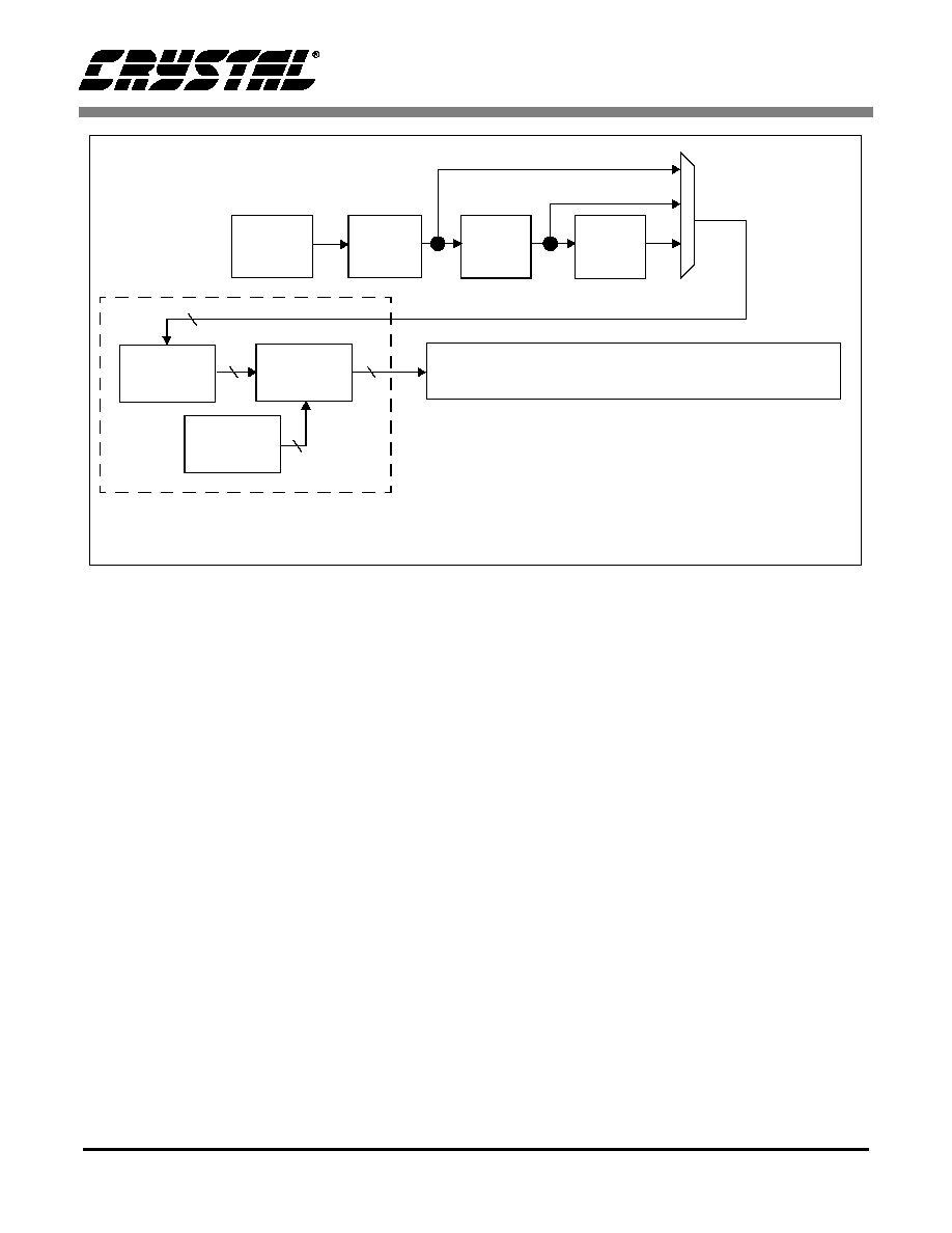
CS5376
DS256PP1
65
9. GAIN AND OFFSET CORRECTION
The CS5376 can apply gain and offset corrections
to the digitally filtered data in each measurement
channel. Gain correction uses scaling values writ-
ten to the GAIN registers (0x21-0x24), while offset
correction uses values written to the OFFSET reg-
isters (0x25-0x28).
In addition to the gain and offset corrections, an
offset calibration algorithm is included in the
CS5376 that automatically calculates offset correc-
tion values for each channel and writes them into
the OFFSET registers.
9.1 Gain Correction
Gain correction in the CS5376 is used to normalize
sensor gain across multi-sensor networks. It re-
quires externally calculated scale values to be writ-
ten into the GAIN1, GAIN2, GAIN3, and GAIN4
registers.
Gain correction values are 24-bit 2's complement
values with unity gain defined as full scale,
0x7FFFFF (decimal 8388607). Gain correction is
always a fractional multiplication, and can never
gain the digital filter data greater than one.
Output Value = Data * (GAIN / 0x7FFFFF)
Unity Gain: GAIN = 0x7FFFFF
50% Gain: GAIN = 0x3FFFFF
Zero Gain: GAIN = 0x000000
Once the GAIN registers are written, the USEGR
bit (bit 12) in the FILT_CFG register enables gain
correction.
9.1.1
Gain Register Calculation
The calculation of gain correction values is made
externally to the CS5376, and the results written
into the GAIN registers. Calculated gain correction
values depend on two factors; the minimum gain of
all sensors in the measurement network, and the
relative gain of individual sensors to that minimum
gain.
The relative gain of each sensor is determined by
applying a standardized input signal and measuring
Figure 41. Gain and Offset Correction
FIR
IIR
Filters
Filter
Output to High Speed Serial Data Port (SD Port)
Offset
Correction
Output Rate 62.5 Hz ~ 4 kHz
SINC
Filter
MDI Input
512 kHz
Correction
Gain
Offset
Calibration
4
4
4
4

CS5376
DS256PP1
66
the maximum and minimum data values from the
CS5376.
Relative Gain = [(maximum - minimum) / 2]
The lowest value of relative gain from all sensors in
a measurement network determines a standard gain
value.
Standard Gain = minimum relative gain
The gain correction value for a specific measure-
ment channel is calculated as the value required to
scale that sensor's relative gain down to the stan-
dard gain value.
Gain Correction = [(standard gain / relative gain) *
0x7FFFFF]
Once calculated, a sensor's gain correction value is
written to the GAIN register for that measurement
channel.
9.2 Offset Correction
Offset correction in the CS5376 is used to cancel
the DC bias in a measurement channel. It uses val-
ues from the OFFSET1, OFFSET2, OFFSET3, and
OFFSET4 registers to shift the output data and
eliminate systematic offsets. Offset correction val-
ues are 24-bit 2's complement with a maximum
positive value of 0x7FFFFF (decimal 8388607),
and a maximum negative value of 0x800000 (deci-
mal 8388608).
Calculation of offset correction values is performed
manually using output data from each channel, or
automatically using the internal offset calibration
algorithm. When offset correction values are calcu-
lated manually, they must be written into the OFF-
SET registers. When using the offset calibration
algorithm, the calculated offset correction values
are written to the OFFSET registers automatically.
Once the OFFSET registers are written, the USE-
OR bit (bit 13) in the FILT_CFG register enables
offset correction.
Offset correction is a simple subtraction of the off-
set correction value from the output data, with
overflow protection ensuring the corrected value
does not exceed the maximum limits. If offset cor-
rection causes the output data to exceed a 24-bit 2's
complement maximum, the output data value will
saturate.
Output Value = Data - Offset Correction
Max Positive Output Value = 0x7FFFFF
Max Negative Output Value = 0x800000
9.2.1
Offset Register Calculation
An offset correction value manual calculation uses
output data from the CS5376 when no signal is in-
put to the sensor. Background noise measurements
are averaged to determine the DC bias present in
the measurement channel.
DC Offset = [Sum(Noise Data) / Num Data]
Once determined, the manually calculated offset
correction value is written to the OFFSET register
for that channel.
9.3 Offset Calibration
An offset calibration algorithm is included in the
CS5376 to automatically calculate offset correction
values. When using the offset calibration algo-
rithm, no signal should be present on the sensor.
Background noise data is used to calculate an aver-
age offset value for each measurement channel.
Offset calibration is an exponential averaging func-
tion that places increased weight on current input
samples. The exponential weighting factor is set by
the EXP bits (bits 16-20) in the FILT_CFG regis-
ter. Increasing the exponent value applies greater
weight to earlier samples and produces a smoother
averaging function requiring a longer settling time.
Decreasing the exponent value applies greater
weight to later samples and produces a noisier av-
eraging function requiring a shorter settling time.
Typical exponential values range from 0x05 to

CS5376
DS256PP1
67
0x0F (decimal 5 to 15), depending on the available
time to settle the algorithm.
Once the EXP bits are written, the ORCAL bit (bit
14) in the FILT_CFG register is set to enable offset
calibration. When enabled, background noise mea-
surements are averaged using the exponential aver-
aging routine, with updated offset correction values
automatically written to the OFFSET registers.
When the exponential algorithm settles the OR-
CAL bit is cleared to disable offset calibration, and
the values in the OFFSET registers are no longer
updated. The last values written to the OFFSET
registers are used as the final offset correction val-
ues.
The characteristic equations for the exponential
offset calibration algorithm include an input value,
X, an output value, Y, a summation value, YSUM,
a sample index, n, and an exponential value, N.
Y(n) = X(n) - [YSUM(n-1) >> N]
YSUM(n) = Y(n) + YSUM(n-1)
Offset Correction = YSUM >> N

CS5376
DS256PP1
68
9.3.1
FILT_CFG Register
(MSB) 23
22
21
20
19
18
17
16
--
--
--
EXP4
EXP3
EXP2
EXP1
EXP0
R/W
R/W
R/W
R/W
R/W
R/W
R/W
R/W
0
0
0
0
0
0
0
0
15
14
13
12
11
10
9
8
--
ORCAL
USEOR
USEGR
--
FSEL2
FSEL1
FSEL0
R/W
R/W
R/W
R/W
R/W
R/W
R/W
R/W
0
0
0
0
0
0
0
0
7
6
5
4
3
2
1
(LSB) 0
--
DEC2
DEC1
DEC0
--
--
CH1
CH0
R/W
R/W
R/W
R/W
R/W
R/W
R/W
R/W
0
0
0
0
0
0
0
0
I/O Address: 0x20
--
Not defined;
read as 0
R
Readable
W
Writable
R/W
Readable and
Writable
Bits in bottom rows
are reset condition
Bit definitions:
23:21 --
reserved
15
--
reserved
7
--
reserved
21:16 EXP[4:0] DC Offset Calibration
Routine Exponent
(Determines sensitivity
of DC offset calibration
routine)
14
ORCAL
Offset Register Calibra-
tion Routine Enable
1: enabled
0: disabled
6:4
DEC[2:0]
Decimation Rate, Output
Word Rate
111: 4 kHz
110: 2 kHz
101: 1 kHz
100: 500 Hz
011: 333.3 Hz
010: 250 Hz
001: 125 Hz
000: 62.5 Hz
13
USEOR
Use Offset Register Cor-
rection
1: enabled
0: disabled
3:2
--
reserved
12
USEGR
[11:8]
Use Gain Register Cor-
rection
1: enabled
0: disabled
1:0
CH[1:0]
Channel Enable
11: 3 Channel (1, 2, 3)
10: 2 Channel (1, 2)
01: 1 Channel (1 only)
00: 4 Channel (1, 2, 3, 4)
11
--
reserved
10:8
FSEL[2:0] Output Filter Select
111: reserved
110: reserved
101: IIR 3rd Order
100: IIR 2nd Order
011: IIR 1st Order
010: FIR2 Output
001: FIR1 Output
000: Sinc Output
Figure 42. Filter Configuration Register FILT_CFG

CS5376
DS256PP1
69
9.3.2
GAIN1 - GAIN4 Registers
(MSB) 23
22
21
20
19
18
17
16
GAIN23
GAIN22
GAIN21
GAIN20
GAIN19
GAIN18
GAIN17
GAIN16
R/W
R/W
R/W
R/W
R/W
R/W
R/W
R/W
0
0
0
0
0
0
0
0
15
14
13
12
11
10
9
8
GAIN15
GAIN14
GAIN13
GAIN12
GAIN11
GAIN10
GAIN9
GAIN8
R/W
R/W
R/W
R/W
R/W
R/W
R/W
R/W
0
0
0
0
0
0
0
0
7
6
5
4
3
2
1
(LSB) 0
GAIN7
GAIN6
GAIN5
GAIN4
GAIN3
GAIN2
GAIN1
GAIN0
R/W
R/W
R/W
R/W
R/W
R/W
R/W
R/W
0
0
0
0
0
0
0
0
I/O Address: 0x21
--
Not defined;
read as 0
R
Readable
W
Writable
R/W
Readable and
Writable
Bits in bottom rows
are reset condition
Figure 43. Gain Correction Register GAIN1
Bit definitions:
23:16 GAIN[23:16]
Gain Correction
Upper Byte
15:8
GAIN[15:8]
Gain Correction
Middle Byte
15:8
GAIN[7:0]
Gain Correction
Lower Byte

CS5376
DS256PP1
70
9.3.3
OFFSET1 - OFFSET4 Registers
(MSB) 23
22
21
20
19
18
17
16
OFST23
OFST22
OFST21
OFST20
OFST19
OFST18
OFST17
OFST16
R/W
R/W
R/W
R/W
R/W
R/W
R/W
R/W
0
0
0
0
0
0
0
0
15
14
13
12
11
10
9
8
OFST15
OFST14
OFST13
OFST12
OFST11
OFST10
OFST9
OFST8
R/W
R/W
R/W
R/W
R/W
R/W
R/W
R/W
0
0
0
0
0
0
0
0
7
6
5
4
3
2
1
(LSB) 0
OFST7
OFST6
OFST5
OFST4
OFST3
OFST2
OFST1
OFST0
R/W
R/W
R/W
R/W
R/W
R/W
R/W
R/W
0
0
0
0
0
0
0
0
I/O Address: 0x25
--
Not defined;
read as 0
R
Readable
W
Writable
R/W
Readable and
Writable
Bits in bottom rows
are reset condition
Figure 44. Offset Correction Register OFFSET1
Bit definitions:
23:16 OFST[23:16]
Offset Correction
Upper Byte
15:8
OFST[15:8]
Offset Correction
Middle Byte
15:8
OFST[7:0]
Offset Correction
Lower Byte

CS5376
DS256PP1
71
10. SERIAL DATA OUTPUT PORT
After digital filtering is completed, each 24-bit out-
put sample is combined with an 8-bit status word.
This 32-bit data word is written to an 8-deep FIFO
buffer and then transmitted to the communications
interface through the high speed serial data output
port (SD port).
The buffering provided by the SD port data FIFO
relaxes the timing requirements for polling conver-
sion data from the CS5376. When running a 4-
channel digital filter, the communications control-
ler can delay up to 2 output periods before request-
ing data from the SD port. A 1-channel or 2-
channel system has even longer delays before the
FIFO data is overwritten.
10.1 SD Port Pin Descriptions
SDTKI - Pin 64
Input signal which will initiate SDRDY signaling
to start an SD port transaction.
SDRDY - Pin 61
Signal which goes low to indicate that 32-bit con-
version words are available to be clocked out of the
SDDAT pin.
SDCLK - Pin 62
Input clock which determines the rate at which the
SDDAT bits are output. Data is valid on rising edg-
es of SDCLK, and transitions on falling edges.
SDDAT - Pin 60
Serial data output for conversion words from the
CS5376. Formatted to output a 32-bit digital word
consisting of one status byte followed by a three
byte conversion word.
SDTKO - Pin 63
Output signal which indicates the current SD port
transaction has been completed.
Figure 45. Serial Data Output Port Pins
SDTKI - Serial Data Chip Select Input, pin 64
Input signal which will initiate SDRDY signaling to start an SD port transaction.
SDRDY - Serial Data Ready Output, pin 61
Signal which goes low to indicate that 32-bit conversion words are available to be
clocked out of the SDDAT pin.
SDCLK - Serial Data Clock Input, pin 62
Input clock which determines the rate at which the SDDAT bits are output. Data is
valid on rising edges of SDCLK, and transitions on falling edges.
SDDAT - Serial Data Output, pin 60
Serial data output for conversion words from the CS5376. Formatted to output a 32-bit
digital word consisting of one status byte followed by a three byte conversion word.
SDTKO - Serial Data Chip Select Output, pin 63
Output signal which indicates the current SD port transaction has been completed.
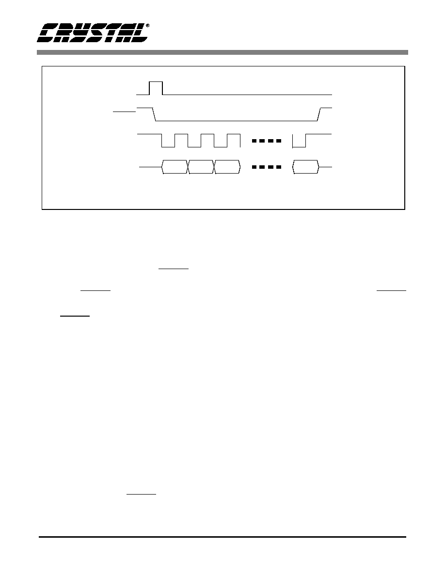
CS5376
DS256PP1
72
10.2 Serial Data Transactions
To initiate a serial data output port transaction, the
SDTKI chip select pin must receive a rising edge.
If output data words are available in the data FIFO,
the CS5376 immediately pulls the SDRDY pin low
to signal the start of an SD port transaction. The SD
port holds SDRDY low until all data has been
clocked from the data FIFO.
Once SDRDY goes low, the communications con-
troller pulls 32-bit data words MSB first from the
SDDAT output pin by clocking the SDCLK input
pin. Serial data on the SDDAT output pin is valid
on the rising edge of SDCLK, and transitions on the
falling edge. The first eight data bits are a status
byte that indicates the channel number, the time
break flag, and any error conditions. The status
byte is followed by 24 bits of two's complement
conversion data for the indicated channel. For sys-
tems that don't require status information, the sta-
tus byte can be ignored by receiving the 32 bit data
word into a 24-bit shift register. Clocking 32 bits
into a 24-bit register causes the status bits to shift
out the end.
When the last available data bit is clocked from the
SD port data FIFO, the SDRDY pin returns high
and the SDTKO pin will pulse to signal the end of
the SD port transaction. SDTKO can be used to sig-
nal the communications controller of the end of a
transaction, or can be used to daisy chain multiple
CS5376 devices into a simple token ring by con-
necting it to the SDTKI pin of another CS5376 de-
vice.
If the SDTKI pin receives a rising edge and no
words are available in the data FIFO, the SDRDY
pin remains high and the SDTKO output pin is
pulsed immediately.
10.3 SD Port Configurations
The SD port can operate in two configurations, a
continuous output configuration where data is out-
put immediately when ready, or a requested output
configuration where data is output only when
polled by the communications controller.
Continuous Output Configuration
The continuous output SD port configuration re-
quires the SDTKI pin to receive continuous rising
edges. A simple method for generating rising edg-
es on SDTKI is to connect it to a 4 MHz or slower
system clock. Whenever output data is available
from the decimation engine, a rising edge on SDT-
KI initiates an SD port transaction.
Once an SD port transaction is initiated, the SDTKI
signal must be gated off to ensure no rising edges
SDRDY
SDCLK
SDDAT
Figure 46. Serial Data Output Port Transaction
MSB
LSB
SDTKI

CS5376
DS256PP1
73
occur during the transaction. The easiest way to
guarantee this is to gate the SDTKI input signal
with the SDRDY output signal using an AND gate.
When an SD port transaction is initiated, the
SDRDY signal is driven low by the CS5376 which
gates off the SDTKI input. When the SD port trans-
action is complete, the SDRDY signal automatical-
ly returns high to re-enable the SDTKI input.
Requested Output Configuration
When using the SD port in a requested output con-
figuration, a single pulse to the SDTKI pin initiates
an SD port transaction. The pulse is generated by a
controller that schedules the data into the commu-
nication network. Because data is requested only
when the controller is ready to receive, local data
buffering between the CS5376 and the communica-
tion network is not required.
Once the SD port transaction is completed, the
SDTKO output pin automatically generates a pulse
that can trigger the SDTKI pin of another CS5376.
In this way a pulse `token' started by the communi-
cations controller can pass through a series of dai-
sy-chained CS5376 devices, initiating SD port
transactions in each. The final CS5376 SDTKO
output can be returned to the controller to signal the
end of a polling cycle.
10.4 SD Port Data Format
Each serial transaction is composed of a series of
32-bit words. The first 8 bits of each word are status
information containing an MFLAG indicator,
channel number bits, a time break flag, and a port
overflow flag. The last 24 bits of each output word
are the conversion data for the indicated channel.
The status and data sections of an output word are
shown in Figure 47.
MFLAG Indicator Bit - MFLAG
The MFLAG indicator is set whenever the
MFLAG signal is received from the modulators on
the MFLAG1-MFLAG4 pins. Each conversion
channel has an independent MFLAG input, and the
MFLAG indicator is independently set in the out-
put word for each channel.
Data
Status
0
23
31
--
MFLAG
CH[1]
CH[0]
W
31
29
30
28
27
26
25
24
Figure 47. SD Port Output Words
TB
--
Word 1
Word 4
Word 2
Word 3
Status
Data
128 bits
--
00 - Channel 1
01 - Channel 2
10 - Channel 3
11 - Channel 4

CS5376
DS256PP1
74
No delay occurs between receiving the MFLAG
signal from the modulators and being output in the
SD port status word. Depending on the group delay
of the digital filters, the invalid data from the mod-
ulator will not be output for several conversion
words after receiving the MFLAG signal. Also, af-
ter recovery of the modulator and clearing of the
MFLAG signal, some number of conversion words
are required before the digital filter will again out-
put valid data.
See "Modulator Data Interface" on page 49 for
more information about the MFLAG signal from
the modulators.
Channel Number Bits - CH[1:0]
The channel number bits indicate which conversion
channel the data word is from. One CS5376 can fil-
ter data for up to four modulators, the channel num-
ber field encodes which modulator the current data
word is from. Note that the channel number,
CH[1:0], is zero based.
·
CH[1:0] = 00 = Channel 1
·
CH[1:0] = 01 = Channel 2
·
CH[1:0] = 10 = Channel 3
·
CH[1:0] = 11 = Channel 4
Time Break Flag - TB
The time break flag marks a timing reference in the
output data stream. When a rising edge is received
on the TIMEB pin a time break event is initiated.
The decimation engine writes the TB flag in the
status byte of the SD port output after a delay pro-
grammed in the TIMEBRK register (0x29). The
TB flag is set in one output word for all enabled
conversion channels. See "Time Break Function"
on page 75 for more information about how the
time break function is used as a timing reference.
Port Overflow Flag - W
The port overflow flag indicates an overflow con-
dition in the SD port data FIFO, and is set by hard-
ware when the decimation engine overwrites a
FIFO register whose data has not been sent. The W
flag is independently set for each output word and
channel.
Conversion Data Word
The last 24 bits of the SD port output word is the
conversion data for the specified channel. The con-
version data is a 24-bit two's complement value.
See "Digital Decimation Filter" on page 53 for
more information how conversion data is generated
in the digital filters.

CS5376
DS256PP1
75
11. TIME BREAK FUNCTION
A time break event places a timing reference flag in
the output data stream. This flag is used during
post-processing to assign an absolute timing to the
digital samples and to time sync data from multiple
measurement channels.
To use the time break function, an externally gen-
erated timing reference signal is applied to the
TIMEB pin to initiate an internal sample counter.
After a certain number of output samples, pro-
grammed in the TIMEBRK register (0x29), the TB
flag is set in the status byte of the output data word
of all enabled channels. The TB flag is automatical-
ly cleared for the next data word, and appears for
only one output sample in each channel.
The programmable sample counter compensates
for group delay through the digital filters. When the
proper group delay is programmed into the TIME-
BRK register, the TB flag is set in the output data
word representing the instant the timing reference
signal was received. Without compensation for
group delay, the TB flag would be set in the output
data word immediately upon receipt and would
precede the sample for the timing reference signal.
11.1 Time Break Pin Description
TIMEB - Pin 57
Time break input pin. A rising edge on the TIMEB
pin signals the decimation engine to set the time
break (TB) flag in the output status word for the
sample representing the current sampling instant.
The rising edge can occur asynchronously to the
CS5376 and is handled as a priority interrupt. To
guarantee the time break input is recognized by the
CS5376, it should be held a minimum of one mas-
ter clock period, nominally 32.768 MHz.
11.2 Time Break Delay
The TIMEBRK register (0x29) sets the delay be-
tween receiving the rising edge on the TIMEB pin
and output of the TB flag in the data stream. The
delay through the CS5376 digital filters depends on
several factors; the sinc filter decimation rate, the
number of coefficients in FIR1 and FIR2, and the
delay through the IIR filters.
The total group delay can be determined empirical-
ly by applying the timing reference signal rising
edge to both the TIMEB pin and the modulator an-
alog inputs. When a rising edge is received on the
TIMEB pin with no delay programmed into the
TIMEBRK register, the TB flag is set immediately
in the next output data word. After some delay, the
rising edge on the modulator inputs will be seen in
the output data stream. The total group delay of the
measurement channel is the number of samples be-
tween the TB flag being set and the appearance of
the impulse in the data stream.
11.3 TB Flag Output
The time break flag (TB flag) marks the timing ref-
erence in the output data stream. The decimation
engine writes the TB flag to the status byte of the
SD port. The TB flag is set in all enabled conver-
sion channels for one output data word. See "Serial
Data Output Port" on page 71 for more information
about the SD port status byte.
Figure 48. Time Break Pin
TIMEB - Time Break, pin 57
Time break input. Signals the decimation engine to set the time break (TB) flag in the
output status word for the sample representing the current sampling instant.

CS5376
DS256PP1
76
11.3.1
TIMEBRK Register
(MSB) 23
22
21
20
19
18
17
16
TBRK23
TBRK22
TBRK21
TBRK20
TBRK19
TBRK18
TBRK17
TBRK16
R/W
R/W
R/W
R/W
R/W
R/W
R/W
R/W
0
0
0
0
0
0
0
0
15
14
13
12
11
10
9
8
TBRK15
TBRK14
TBRK13
TBRK12
TBRK11
TBRK10
TBRK9
TBRK8
R/W
R/W
R/W
R/W
R/W
R/W
R/W
R/W
0
0
0
0
0
0
0
0
7
6
5
4
3
2
1
(LSB) 0
TBRK7
TBRK6
TBRK5
TBRK4
TBRK3
TBRK2
TBRK1
TBRK0
R/W
R/W
R/W
R/W
R/W
R/W
R/W
R/W
0
0
0
0
0
0
0
0
I/O Address: 0x29
--
Not defined;
read as 0
R
Readable
W
Writable
R/W
Readable and
Writable
Bits in bottom rows
are reset condition
Figure 49. Time Break Counter Register TIMEBRK
Bit definitions:
23:16 TBRK[23:16] Time Break Counter
Upper Byte
15:8
TBRK[15:8] Time Break Counter
Middle Byte
15:8
TBRK[7:0]
Time Break Counter
Lower Byte

CS5376
DS256PP1
77
12. SYSTEM SYNCHRONIZATION
In many applications the CS5376 is used to create
a distributed measurement network. To be useful,
data sets from multiple sensors in a network must
have a known timing relationship between them.
Synchronous multi-sensor data can be combined
during post-processing to provide much more in-
formation than data from only a single sensor. To
establish a standardized timing relationship be-
tween sensors, the CS5376 can be synchronized
with the external network.
12.1 Synchronous Clocking
The CS5376 uses an input clock of 32.768 MHz
and divides it down to generate internal clock fre-
quencies of 8.192 MHz, 4.096 MHz, 2.048 MHz,
1.024 MHz, 512 kHz, 256 kHz, 128 kHz, and 32
kHz. Clock rates for the decimation engine, watch-
dog timer, sinc filter, and modulator are selected
from these generated clocks via the CONFIG reg-
ister (0x00).
When the input clock is synchronous to the external
network, the internal clocks of the CS5376 will
also be synchronous. A synchronous input clock
can only be guaranteed by careful design of clock
distribution in the external network. See "System
Design" on page 13 for more information about the
design requirements for a synchronous clock distri-
bution network.
12.2 Synchronization Signals
In addition to synchronous clocking, the signal
measurement and analysis functions should be
phase aligned. To accomplish this the CS5376 has
a synchronization input pin, SYNC, that phase
aligns the modulator clocks and digital filters.
Clock Divider
CLK
CONFIG Register
MCLK
Internal
Clocks
Figure 50. Clock and MSYNC Generation
MSYNC
SYNC
Decimation
and
Generator
MSYNC
Engine
Figure 51. Synchronization Pins
SYNC - Device Synchronization Input Signal, pin 59
Input synchronization signal. MSYNC is generated from a rising edge on this pin to
synchronize the modulators, sinc filter, and decimation engine.
MSYNC - Modulator Sync Output, pin 14
A transition from logic low to high reinitializes the modulator timing to be synchronous
with the timing of the CS5376. Generated from the SYNC input signal.

CS5376
DS256PP1
78
The SYNC signal must be distributed across a net-
work so that it arrives at every measurement node
simultaneously. This can only be guaranteed by
careful design of the SYNC signal distribution in
the network. See "System Design" on page 13 for
more information about the design requirements
for the SYNC signal in an external network.
12.3 CS5376 Internal Synchronization
The SYNC signal rising edge is used to generate an
internal re-timed synchronization signal, MSYNC,
as shown in Figure 52. The MSYNC signal is used
internally to reinitialize the sinc filters, decimation
engine, serial data output port, time break counter,
and test bit stream generator. It is also output to the
MSYNC pin to phase align the modulator sampling
instants, giving precise sample timing across the
network.
The MSEN bit in the CONFIG register (0x00) en-
ables MSYNC generation. When MSEN is en-
abled, the MSYNC output signal is generated and
MSYNC is used as an internal synchronization sig-
nal when a rising edge is detected on the SYNC pin.
When MSEN is disabled, the MSYNC output re-
mains low and the internal blocks are not affected
by the SYNC signal.
12.3.1 Sinc Filter Synchronization
The sinc filters use the rising edge of MSYNC to
reset the internal state machine and data pointers.
While the data pointers used to access the sinc filter
registers are reset, the registers themselves are not
cleared. The initial output data from the sinc filters
after an MSYNC event will be a combination of
pre-sync and post-sync data. Valid data is output
once all the sinc filter registers have been overwrit-
ten with new data.
MSYNC
MCLK
MDATAx
Figure 52. SYNC and MSYNC Timing
(2.048 MHz)
t
msd
t
msd
(512 kHz)
t
msh
Note: MDATA at 256 kHz has the same start timing, but takes 8 MCLK cycles to update.
Data1
Data2
t
msd
= T
MCLK
/ 4
t
msh
= T
MCLK
For f
MCLK
= 2.048 MHz:
t
msd
= 122 ns
t
msh
= 488 ns
SYNC

CS5376
DS256PP1
79
12.3.2 Decimation Engine Synchronization
The decimation engine uses the rising edge of
MSYNC to reset the FIR filter data pointers. Simi-
lar to the sinc filters, the FIR data pointers are reset
but the data registers themselves are not cleared.
After an MSYNC event the initial output data from
the FIR filters will be a combination of pre-sync
and post-sync data. Valid data is output once all
data registers have been overwritten with new data.
Note that the IIR filters are not directly affected by
a synchronization event, but will require time to
settle due to the FIR filter output discontinuity.
12.3.3 SD Port Synchronization
The serial data output port uses the rising edge of
MSYNC to re-initialize the output data FIFO. Both
the write and read pointers are reset, and the data
registers are cleared. The CS5376 requires one out-
put period to pass after an MSYNC event before
data is available from the SD port.
12.3.4 Time Break Synchronization
The time break function is disabled by a MSYNC
event since MSYNC disturbs filter operations. The
time break timing reference in the output data
stream depends on the group delay of the digital fil-
ters. When a synchronization event occurs, the fil-
ter group delay is no longer consistent which
renders the time break delay invalid.
The rising edge of MSYNC automatically clears
the current time break countdown value and dis-
ables the time break output flag, but does not affect
the programmed counter initialization value in the
TIMEBRK register (0x29).
12.3.5 Test Bit Stream Synchronization
When the test bit stream generator is enabled, the
rising edge of an MSYNC signal resets the TBS
data pointer. This restarts the test bit stream from
the first data point, and establishes a known phase
in the output signal.
In the internal test bit stream data set, the first data
point is the initial positive going data value of a
1024 point sine wave. An MSYNC event will
therefore restart the test bit stream generator at zero
degrees phase when using the internal data set.
The first data value of a custom test bit stream data
set can be defined to be anywhere in the test signal.
This permits setting the test bit stream generator
output phase by defining the first data point to be a
non-zero degree phase of the test signal.
12.4 Modulator Synchronization
The generated MSYNC signal is used internally to
synchronize the CS5376, but is also output to the
MSYNC pin to phase align the modulator sam-
pling. Since high precision modulators such as the
CS5372 require multiple MCLK phases to com-
plete a conversion, unsynchronized modulators can
have random sampling instants relative to each oth-
er. The MSYNC signal guarantees all modulators
in a network have the same sampling instant.

CS5376
DS256PP1
80
12.4.1
CONFIG Register
(MSB)23
22
21
20
19
18
17
16
--
--
--
--
--
DFS2
DFS1
DFS0
R/W
R/W
R/W
R/W
R/W
R/W
R/W
R/W
0
0
0
0
0
1
0
1
15
14
13
12
11
10
9
8
--
WDFS2
WDFS1
WDFS0
--
MCKFS2
MCKFS1
MCKFS0
R/W
R/W
R/W
R/W
R/W
R/W
R/W
R/W
0
0
0
0
0
1
0
0
7
6
5
4
3
2
1
(LSB)0
--
--
MCKEN2
MCKEN
MDIFS
SBY
BOOT
MSEN
R/W
R/W
R/W
R/W
R/W
R/W
R
R/W
0
0
0
0
0
0
0
1
Figure 53. Decimation Engine Configuration Register CONFIG
Bit definitions:
23:19 --
reserved
15
--
reserved
7:6
--
reserved
18:16 DFS
[2:0]
Decimation Engine
Frequency Select
111: reserved
110: 8.192 MHz
101: 4.096 MHz
(default)
100: 2.048 MHz
011: 1.024 MHz
010: 512 kHz
001: 256 kHz
000: 32 kHz
14:12 WDFS
[2:0]
Watchdog Frequency
Select
111: reserved
110: 8.192 MHz
101: 4.096 MHz
100: 2.048 MHz
011: 1.024 MHz
010: 512 kHz
001: 256 kHz
000: 32 kHz (default)
5
MCKEN2
MCLK/2 Output Enable
4
MCKEN
MCLK Output Enable
3
MDIFS
MDI Frequency Select:
1: 256 kHz
0: 512 kHz (default)
2
SBY
Standby
1: DE in low power, low
frequency mode
0: DE normal operation
11
--
reserved
10:8
MCKFS
[2:0]
MCLK Frequency Select
111: reserved
110: reserved
101: 4.096 MHz
100: 2.048 MHz
(default)
011: 1.024 MHz
010: 512 kHz
001: reserved
000: reserved
1
BOOT
Boot Source Select
1: Boot from PROM
0: Boot from SPI
0
MSEN
MSYNC Enable
1: MSYNC is generated
from SYNC
0: MSYNC remains low
I/O Address: 0x00
--
Not defined;
read as 0
R
Readable
W
Writable
R/W
Readable and
Writable
Bits in bottom rows
are reset condition

CS5376
DS256PP1
81
13. TEST BIT STREAM GENERATOR
The CS5376 includes a test bit stream (TBS) gen-
erator designed to drive an off-chip test DAC. The
TBS output can also be internally connected to the
digital filter input for loopback testing.
The test bit stream generator output is programma-
ble and the exact configuration depends on the type
of test DAC used. When used in digital loopback
mode the output will be 1-bit at 512 kHz. Many test
signal frequencies between 2 Hz and 125 Hz (in-
cluding 31.25 Hz) can be generated using the inter-
nal data set. Test frequencies between 2 Hz and 125
Hz that cannot be generated using the internal data
set can be generated by writing a custom data set.
13.1 TBS Generator Architecture
The test bit stream generator incorporates a data in-
terpolation module and a digital
- modulator
which receives periodic 24-bit input data from the
decimation engine. The test bit stream generator
outputs a data clock to the TBSCLK pin and a 1-bit
- modulated bit stream to the TBSDATA pin.
The test bit stream generator runs from an internal
clock set in the TBS_CFG register (0x2A). The
output clock rate on the TBSCLK pin is 1/8 the se-
lected internal clock rate. A delay can be intro-
duced to the output clock to align it with any rising
edge of the internal clock, a resolution of 1/8 the
output clock period. Data output from the TBSDA-
TA pin also has a programmable delay, up to 64 in-
ternal clock periods.
13.2 TBS Pin Descriptions
TBSCLK - Pin 8
Test bit stream output clock. Output rate is 1/8 the
programmed internal test bit stream generator
clock rate. Can be delayed up to 8 internal clock pe-
riods.
TBSDATA - Pin 9
Test bit stream output data. Can be delayed up to 64
internal clock periods.
Loopback - Internal
Internal connection providing a data path from the
test bit stream generator output to the digital filter
input.
Digital
Modulator
24b @ 64 Fs
1b @ 512 Fs
TBSDATA
Decimation Engine
Interpolator
24b @ 1 Fs
Figure 54. Digital TBS Data Path
Data Bus
Figure 55. Test Bit Stream Pins
TBSCLK - Test Signal Modulator Clock Output, pin 8
A dedicated clock output pin to interface with an external
- test DAC.
TBSDATA - Test Signal Modulator Data Output, pin 9
A dedicated data output pin to interface with an external
- test DAC.

CS5376
DS256PP1
82
13.3 TBS Data Source
When enabled, the TBS generator has input data
periodically written by the decimation engine. The
source of the data can either be an internal 1024
point sine-wave or a user programmed data set of
up to 1024 points.
13.3.1 TBS ROM Data
The CS5376 has a 24-bit 1024 point digital sine-
wave stored internally. This data can be specified
to be used by the test bit stream generator during
the initial boot configuration of the CS5376. Both
the coprocessor and stand-alone boot modes in-
clude a command, `Write TBS ROM Data', to ini-
tialize the internal data set for use by the test bit
stream generator. See "Serial Peripheral Interface
1" on page 21 for information about boot modes
and configuration commands.
Using the internal data set, the TBS generator can
produce many test signal frequencies between 2 Hz
and 125 Hz. When used in digital loopback mode,
the TBS generator produces a 1-bit 512 kHz output
bit stream suitable for the digital filter input. Figure
56 lists selected test signal frequencies that can be
generated for digital filter loopback using the in-
cluded TBS data set. Other test frequencies and
output rates can be programmed using the internal
data set by varying the internal clock rate and inter-
polation factor.
13.3.2 TBS Uploaded Data
If a specific test frequency is required that cannot
be generated using the internal test bit stream data
set, a custom data set can be written into the
CS5376. Both the coprocessor and stand-alone
boot modes include a command, `Write TBS Data',
to write a custom TBS data set up to 1024 points.
The number of data points written will depend on
the test signal frequency to be generated, the re-
quired output clock frequency, and the available in-
terpolation factors. Note that any custom data set
must be continuous on the ends; i.e. when copied
end-to-end the data set must produce a smooth
curve.
13.4 TBS Configuration
After a TBS data source has been specified, the test
bit stream generator is configured by writing the
TBS_CFG register (0x2A).
Figure 56. Selected TBS Settings for 512 kHz Output
Test Signal
Frequency
(TBSDATA)
Output Clock
Rate
(TBSCLK)
Internal Clock
Rate
(RATE)
Interpolation
Factor
(INTP)
2.00 Hz
512 kHz
4.096 MHz
0xF9
5.00 Hz
512 kHz
4.096 MHz
0x63
10.00 Hz
512 kHz
4.096 MHz
0x31
25.00 Hz
512 kHz
4.096 MHz
0x13
31.25 Hz
512 kHz
4.096 MHz
0x0F
33.33 Hz
512 kHz
4.096 MHz
0x0E
50.00 Hz
512 kHz
4.096 MHz
0x09
62.50 Hz
512 kHz
4.096 MHz
0x07
100.00 Hz
512 kHz
4.096 MHz
0x04
125.00 Hz
512 kHz
4.096 MHz
0x03

CS5376
DS256PP1
83
13.4.1 Interpolation Factor
The INTP bits select how many times the data in-
terpolation module will re-use a data point to gen-
erating the output bit stream. The value is zero
based and so represents one greater than the actual
register value. (0x0F => interpolation by 16).
13.4.2 Clock Rate
The RATE bits set the test bit stream generator in-
ternal clock rate. The output clock and data bit
stream rate from the TBSCLK and TBSDATA pins
are 1/8 of this frequency.
13.4.3 Clock Delay
The CDLY bits program a delay for TBSCLK, up
to 8 internal clock periods.
13.4.4 Loopback Enable
The LOOP bit enables the digital loopback connec-
tion into the digital filters.
13.4.5 Run Enable
The RUN bit enables the test bit stream generator.
13.4.6 Data Delay
The DDLY bits program a delay for TBSDATA,
up to 64 internal clock periods.

CS5376
DS256PP1
84
13.4.7
TBS_CFG Register
(MSB) 23
22
21
20
19
18
17
16
INTP7
INTP6
INTP5
INTP4
INTP3
INTP2
INTP1
INTP0
R/W
R/W
R/W
R/W
R/W
R/W
R/W
R/W
0
0
0
0
0
0
0
0
15
14
13
12
11
10
9
8
--
RATE2
RATE1
RATE0
--
CDLY2
CDLY1
CDLY0
R/W
R/W
R/W
R/W
R/W
R/W
R/W
R/W
0
0
0
0
0
0
0
0
7
6
5
4
3
2
1
(LSB) 0
LOOP
RUN
DDLY5
DDLY4
DDLY3
DDLY2
DDLY1
DDLY0
R/W
R/W
R/W
R/W
R/W
R/W
R/W
R/W
0
0
0
0
0
0
0
0
I/O Address: 0x2A
--
Not defined;
read as 0
R
Readable
W
Writable
R/W
Readable and
Writable
Bits in bottom rows
are reset condition
Figure 57. Test Bit Stream Configuration Register TBS_CFG
Bit definitions:
23:16 INTP[7:0]
Interpolation factor
0xFF: 256
0xFE: 255
...
0x01: 2
0x00: 1 (use once)
15
--
reserved
7
LOOP
Enable Test Bit
Stream Digital
Loopback
6
RUN
Enable Test Bit
Stream
14:12 RATE[2:0]
TBS internal clock
rate
111: 16.384 MHz
110: 8.192 MHz
101: 4.096 MHz
100: 2.048 MHz
011: 1.024 MHz
010: 512 kHz
001: 256 kHz
000: 32 kHz
(default)
Output bit rate is 1/8
of this frequency
5:0
DDLY[5:0]
Data output bit
delay
0x3F: 63 bits
0x3E: 62 bits
.
.
.
0x01: 1 bit
0x00: 0 bits (i.e. no
delay)
11
--
reserved
10:8
CDLY[2:0]
Clock output phase
delay
111: 7/8 period
110: 3/4 period
101: 5/8 period
100: 1/2 period
011: 3/8 period
010: 1/4 period
001: 1/8 period
000: none

CS5376
DS256PP1
85
14. GENERAL PURPOSE I/O PINS
The General Purpose I/O (GPIO) block provides 12
general purpose pins to interface with external
hardware. Each GPIO pin can be configured as an
input or an output, with an internal pull-up resistor
enabled or disabled. Several GPIO pins also double
as chip selects for the SPI 1 and SPI 2 ports. Fig-
ure 58 shows the structure of a bi-directional GPIO
pin with SPI chip select functionality.
Each GPIO pin is programmed by three bits in the
GPCFG0 or GPCFG1 registers. The input or output
data direction is selected by the GP_DIR bits, the
internal pull-ups are enabled or disabled by the
GP_PULL bits, and the data values are set by the
GP_DATA bits. After reset, the GPIO pins are de-
faulted as inputs with pull-up resistors enabled.
14.1 GPIO Input Mode
When reading a value from the GP_DATA bits, the
returned data reports the current state of the pins. If
a pin is externally driven high it reads a logical 1. It
also reads a logical 1 if the pin is not connected
with its pull-up resistor enabled. If a pin is external-
ly driven low it reads a logical 0. It also reads a log-
ical 0 if the pin is not connected with its pull-up
resistor disabled, due to leakage currents.
When a GPIO pin is used as an input, the pull-up
resistor should be disabled to save power if it isn't
required.
14.2 GPIO Output Mode
When a GPIO pin is used as an output to an external
device, the reset configuration as an input with
pull-up resistors enabled results in a logic high out-
put to the external device until it is programmed.
When a GPIO pin is programmed as an output with
a data value of 0, the pin is driven low and the in-
ternal pull-up resistor is automatically disabled.
When programmed as an output with a data value
of 1, the pin is driven high and the pull-up resistor
is inconsequential.
Any GPIO pin can be used as an open-drain output
by setting the data value to 0, enabling the pull-up,
and using the GP_DIR direction bits to control the
pin value. This open-drain output configuration
uses the internal pull-up resistor to pull the pin high
when GP_DIR is set as an input, and drives the pin
low when GP_DIR is set as an output.
14.2.1 GPIO Read In Output Mode
Note that when read the GP_DATA value always
reports the current state of the pins, and a value
written in output mode does not necessarily read
back the same value. If a pin in output mode is writ-
ten as a logical 1, the CS5376 will drive the pin
high. If an external device then forces the pin low,
the read value will reflect the pin state and return a
logical 0. Similarly, if an output pin is written as a
logical 0 but forced high externally, the read value
will reflect the pin state and return a logical 1. In
Figure 58. GPIO Bi-directional Structure and Operation
CS output from SPI
GPIO/CS
GP_DIR
Data bit
GP_DATA
GP_PULL
Pull Up
Logic
R

CS5376
DS256PP1
86
both cases the CS5376 is in contention with the ex-
ternal device and will result in increased power
consumption.
14.3 GPIO Chip Select
When the CS5376 is used as an SPI master GPIO8-
GPIO11 (CS8-CS11) operate as SPI 1 chip selects
and GPIO0-GPIO4 (CS0-CS4) operate as SPI 2
chip selects. The chip select signal from the SPI 1
and SPI 2 blocks are logically AND-ed with the
corresponding GPIO data bit. The GPIO pin should
be set as output mode and a logical 1 to produce the
chip select falling edge required for most serial pe-
ripherals. See "Serial Peripheral Interface 1" on
page 21 and "Serial Peripheral Interface 2" on
page 40 for details on the SPI ports.
14.4 GPIO Pin Descriptions
GPIO0 - GPIO4 (CS0 - CS4) - Pins 32 - 36
The low group of GPIO pins, GPIO0-GPIO4, can
be used as standard GPIO pins or as chip selects for
the SPI 2 port. Each pin can be individually set for
either mode.
When used as standard GPIO pins, the settings are
programmed in the GPCFG0 register. The GP_DIR
bits (bits 16-20) set the input/output mode, the
GP_PULL bits (bits 8-12) enable/disable the inter-
nal pull-up resistor, and the GP_DATA bits (bits 0-
4) set the data value.
When used as SPI 2 chip selects, the GPIO pin
should be programmed in GPCFG0 as output mode
and a logical 1 so the serial device connected to it
will be de-selected by default. When an SPI 2
transaction to the device begins, the GPIO pin au-
tomatically goes low to act as a chip select.
GPIO5 - GPIO7 - Pins 37, 41, 42
The middle group of GPIO pins, GPIO5-GPIO7,
can only be used as standard GPIO pins, and are
programmed in the GPCFG0 register. In the
GPCFG0 register, GP_DIR (bits 20-23) sets the in-
put/output mode, GP_PULL (bits 13-15) en-
ables/disables the internal pull-up resistor, and
GP_DATA (bits 5-7) sets the data value.
GPIO8 - GPIO11 (CS8-CS11) - Pins 43 - 46
The high group of GPIO pins, GPIO8-GPIO11, can
be used as standard GPIO pins or as chip selects for
the SPI 1 port. Each pin can be individually set for
either mode.
When used as standard GPIO pins, the settings are
programmed in the GPCFG1 register. The GP_DIR
bits (bits 16-19) set the input/output mode, the
GP_PULL bits (bits 8-11) enable/disable the inter-
nal pull-up resistor, and the GP_DATA bits (bits 0-
3) set the data value.
When used as SPI 1 chip selects, the GPIO pin
should be programmed in GPCFG1 as output mode
and a logical 1 so the serial device connected to it
will be de-selected by default. When an SPI 1
transaction to the device begins, the GPIO pin au-
tomatically goes low to act as a chip select.
Figure 59. General Purpose I/O Pins
GPIO[11:0] - General Purpose Input/Output, pins 32 to 37, 41 to 46
General purpose pins for controlling local peripherals. Also used as chip selects for the
SPI ports.

CS5376
DS256PP1
87
14.4.1
GPCFG0 Register
(MSB) 23
22
21
20
19
18
17
16
GP_DIR7
GP_DIR6
GP_DIR5
GP_DIR4
GP_DIR3
GP_DIR2
GP_DIR1
GP_DIR0
R/W
R/W
R/W
R/W
R/W
R/W
R/W
R/W
0
0
0
0
0
0
0
0
15
14
13
12
11
10
9
8
GP_PULL7
GP_PULL6
GP_PULL5
GP_PULL4
GP_PULL3
GP_PULL2
GP_PULL1
GP_PULL0
R/W
R/W
R/W
R/W
R/W
R/W
R/W
R/W
1
1
1
1
1
1
1
1
7
6
5
4
3
2
1
(LSB) 0
GP_DATA7
GP_DATA6
GP_DATA5
GP_DATA4
GP_DATA3
GP_DATA2
GP_DATA1
GP_DATA0
R/W
R/W
R/W
R/W
R/W
R/W
R/W
R/W
1
1
1
1
1
1
1
1
I/O Address: 0x0E
--
Not defined;
read as 0
R
Readable
W
Writable
R/W
Readable and
Writable
Bits in bottom rows
are reset condition
Bit definitions:
23:16 GP_DIR
[7:0]
Pin direction
1: output
0: input
15:8
GP_PULL
[7:0]
Pullup resistor
1: enabled
0: disabled
7:0
GP_DATA
[7:0]
Data Value
Figure 60. GPIO Configuration Register GPCFG0
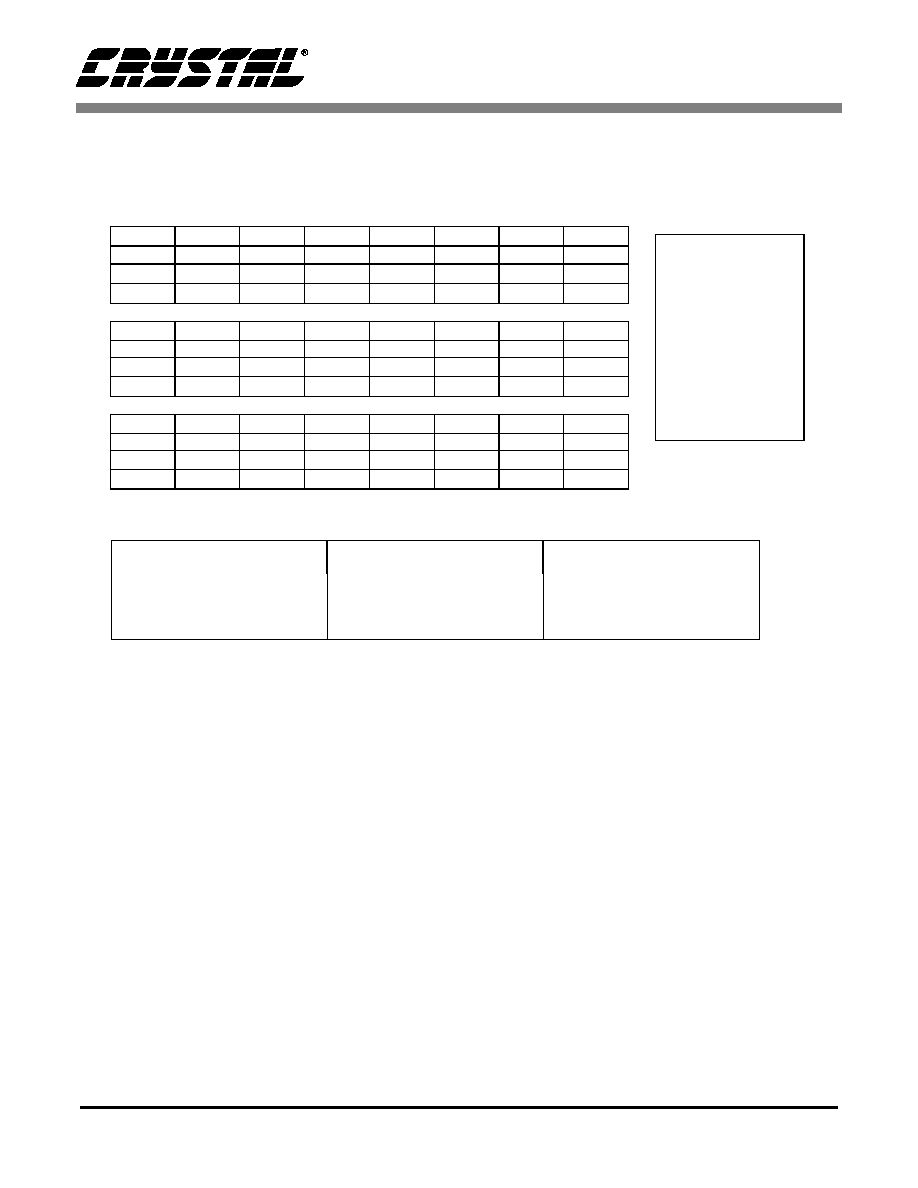
CS5376
DS256PP1
88
14.4.2
GPCFG1 Register
(MSB) 23
22
21
20
19
18
17
16
--
--
--
--
GP_DIR11
GP_DIR10
GP_DIR9
GP_DIR8
R/W
R/W
R/W
R/W
R/W
R/W
R/W
R/W
0
0
0
0
0
0
0
0
15
14
13
12
11
10
9
8
--
--
--
--
GP_PULL11
GP_PULL10
GP_PULL9
GP_PULL8
R/W
R/W
R/W
R/W
R/W
R/W
R/W
R/W
0
0
0
0
1
1
1
1
7
6
5
4
3
2
1
(LSB) 0
--
--
--
--
GP_DATA11
GP_DATA10
GP_DATA9
GP_DATA8
R/W
R/W
R/W
R/W
R/W
R/W
R/W
R/W
0
0
0
0
1
1
1
1
I/O Address: 0x0F
--
Not defined;
read as 0
R
Readable
W
Writable
R/W
Readable and
Writable
Bits in bottom rows
are reset condition
Bit definitions:
23:20 --
reserved
15:12 --
reserved
7:4
--
reserved
19:16 GP_DIR
[11:8]
Pin direction
1: output
0: input
11:8
GP_PULL
[11:8]
Pullup resistor
1: enabled
0: disabled
3:0
GP_DATA
[11:8]
Data Value
Figure 61. GPIO Configuration Register GPCFG1

CS5376
DS256PP1
89
15. JTAG TEST PORT (IEEE 1149.1)
The CS5376 includes a JTAG test port for bound-
ary scan testing. Boundary scan testing checks the
interconnections of a design by writing and reading
data directly from the pins using an on-chip JTAG
controller. For a detailed description of the oper-
ation of the JTAG port, refer to the IEEE 1149.1
specification.
15.1 JTAG Pin Definitions
TRST - Pin 1
Resets the test access port controller and all bound-
ary scan cells in the scan chain. This pin includes a
weak pullup resistor to provide a power on reset if
not driven by a signal source.
TMS - Pin 2
The test mode of the JTAG controller is selected by
a serial write to this pin using TCK.
TCK - Pin 3
Clock input for the test access port controller.
TDI - Pin 4
Serial data input to the boundary scan chain or test
access port controller.
TDO - Pin 5
Serial data output from the boundary scan chain or
test access port controller.
15.2 JTAG Architecture
The JTAG test circuitry consists of a test access
port (TAP) controller and boundary scan cells
within each pin. The boundary scan cells are linked
together to create a scan chain around the CS5376.
15.2.1 TAP Controller
The test access port (TAP) controller manages seri-
al scanning of instruction and data information
through the CS5376. The TAP controller uses the
16 JTAG state assignments from the IEEE 1149.1
specification which are sequenced based on the
state of the TMS pin on the rising edge of TCK.
The TAP controller generates signals for capture,
shift, and update operations on the internal instruc-
Figure 62. JTAG Pins
TRST - Test Reset, pin 1
JTAG reset input pin, resets the test access port controller (TAP).
TMS - Test Mode Select, pin 2
JTAG mode select input pin, control signal to the test access port controller (TAP).
TCK - Test Clock, pin 3
JTAG clock input pin, clocks the test access port controller (TAP).
TDI - Test Data Input, pin 4
JTAG data input pin, the path by which serial data enters the device.
TDO - Test Data Output, pin 5
JTAG data output pin, the path by which serial data exits the device.

CS5376
DS256PP1
90
tion and data registers. In the capture operation,
data is loaded into the internal register. In the shift
operation, the captured data is shifted out while
new data is shifted in. In the update operation, ei-
ther the instruction register is loaded for instruction
decode, or the boundry-scan registers are updated
to control the outputs.
15.2.2 Boundary Scan Cells
Designed into each pin of the CS5376 is a bound-
ary scan cell. In normal operation with the JTAG
disabled, the boundary scan cells are transparent
and do not affect operation of the CS5376. When
using the JTAG port, the boundary scan cells give
the ability to write and read each pin independent
of the CS5376 operation. The boundary scan cells
are serially linked to create a scan chain around the
CS5376.

CS5376
DS256PP1
91
16. WATCHDOG TIMER
A watchdog timer built into the CS5376 can pro-
vide additional system robustness by monitoring
the decimation engine to ensure no unrecoverable
errors occur. If a programmed time period elapses
without the decimation engine automatically re-
starting the watchdog countdown timer, the
CS5376 performs a hardware reset. A hardware re-
set re-boots the system from EEPROM or re-en-
ables communication with the microcontroller,
depending on the boot mode selection.
16.1 Watchdog Timer Initialization
The watchdog timer is initialized by writing two
register values. First, the countdown timer clock
rate is selected in the CONFIG register (0x00), be-
tween 8.192 MHz and 32 kHz. Next, a countdown
value is written to the WD_CFG register (0x2B) to
select the number of clock cycles that must pass be-
fore a hardware reset occurs. After writing the
countdown value, the watchdog timer automatical-
ly starts at the countdown value and rate selected.
A hardware reset is required to exit watchdog mode
once it has been enabled.
As an example, a 1kHz output word rate (1 ms out-
put interval) should allow several milliseconds to
pass before a hardware reset occurs. If the watch-
dog timer clock is set to 1.024 MHz in the CONFIG
register and a countdown value of 0x004000 is
written to the WD_CFG register, a time interval of
16 ms must pass to cause a hardware reset.
16.2 Watchdog Timer Restart
When enabled, the decimation engine restarts the
countdown timer after every filtering algorithm
calculation. Some SPI 1 burst write commands,
(Write FIR Coefficients, Write IIR Coefficients,
and Write TBS Data), do not restart the countdown
timer until after the command has completed. If the
watchdog timer is enabled and an SPI 1 burst write
command does not complete within the countdown
interval, the CS5376 will reset. This recovers the
CS5376 from a state where it expects burst data
that is never written by the microcontroller.
The rate at which the decimation engine automati-
cally restarts the countdown timer depends on the
CS5376 configuration. A faster decimation engine
clock rate and a shorter number of filter coeffi-
cients will restart the countdown timer more quick-
ly. In general, the watchdog timer should be set to
expire if several output data periods pass without
being restarted by the decimation engine.
Output
Word Rate
Output
Interval
Reset
Delay
Watchdog
Clock
Watchdog
Counter
4 kHz
0.25 ms
4 ms
1.024 MHz
0x001000
2 kHz
0.5 ms
8 ms
1.024 MHz
0x002000
1 kHz
1.0 ms
16 ms
1.024 MHz
0x004000
500 Hz
2.0 ms
32 ms
1.024 MHz
0x008000
333.3 Hz
3.0 ms
48 ms
1.024 MHz
0x00C000
250 Hz
4.0 ms
64 ms
512 kHz
0x008000
125 Hz
8.0 ms
128 ms
256 kHz
0x008000
62.5 Hz
16.0 ms
256 ms
256 kHz
0x00FFFF
Figure 63. Watchdog Timer Recommended Settings
CS5376
DS256PP1
92
16.2.1
CONFIG Register
(MSB)23
22
21
20
19
18
17
16
--
--
--
--
--
DFS2
DFS1
DFS0
R/W
R/W
R/W
R/W
R/W
R/W
R/W
R/W
0
0
0
0
0
1
0
1
15
14
13
12
11
10
9
8
--
WDFS2
WDFS1
WDFS0
--
MCKFS2
MCKFS1
MCKFS0
R/W
R/W
R/W
R/W
R/W
R/W
R/W
R/W
0
0
0
0
0
1
0
0
7
6
5
4
3
2
1
(LSB)0
--
--
MCKEN2
MCKEN
MDIFS
SBY
BOOT
MSEN
R/W
R/W
R/W
R/W
R/W
R/W
R
R/W
0
0
0
0
0
0
0
1
Figure 64. Decimation Engine Configuration Register CONFIG
Bit definitions:
23:19 --
reserved
15
--
reserved
7:6
--
reserved
18:16 DFS
[2:0]
Decimation Engine
Frequency Select
111: reserved
110: 8.192 MHz
101: 4.096 MHz
(default)
100: 2.048 MHz
011: 1.024 MHz
010: 512 kHz
001: 256 kHz
000: 32 kHz
14:12 WDFS
[2:0]
Watchdog Frequency
Select
111: reserved
110: 8.192 MHz
101: 4.096 MHz
100: 2.048 MHz
011: 1.024 MHz
010: 512 kHz
001: 256 kHz
000: 32 kHz (default)
5
MCKEN2
MCLK/2 Output Enable
4
MCKEN
MCLK Output Enable
3
MDIFS
MDI Frequency Select:
1: 256 kHz
0: 512 kHz (default)
2
SBY
Standby
1: DE in low power, low
frequency mode
0: DE normal operation
11
--
reserved
10:8
MCKFS
[2:0]
MCLK Frequency Select
111: reserved
110: reserved
101: 4.096 MHz
100: 2.048 MHz
(default)
011: 1.024 MHz
010: 512 kHz
001: reserved
000: reserved
1
BOOT
Boot Source Select
1: Boot from PROM
0: Boot from SPI
0
MSEN
MSYNC Enable
1: MSYNC is generated
from SYNC
0: MSYNC remains low
I/O Address: 0x00
--
Not defined;
read as 0
R
Readable
W
Writable
R/W
Readable and
Writable
Bits in bottom rows
are reset condition

CS5376
DS256PP1
93
16.2.2
WD_CFG Register
(MSB) 23
22
21
20
19
18
17
16
--
--
--
--
--
--
--
--
R/W
R/W
R/W
R/W
R/W
R/W
R/W
R/W
0
0
0
0
0
0
0
0
15
14
13
12
11
10
9
8
WCNT15
WCNT14
WCNT13
WCNT12
WCNT11
WCNT10
WCNT9
WCNT8
R/W
R/W
R/W
R/W
R/W
R/W
R/W
R/W
0
0
0
0
0
0
0
0
7
6
5
4
3
2
1
(LSB) 0
WCNT7
WCNT6
WCNT5
WCNT4
WCNT3
WCNT2
WCNT1
WCNT0
R/W
R/W
R/W
R/W
R/W
R/W
R/W
R/W
0
0
0
0
0
0
0
0
I/O Address: 0x2B
--
Not defined;
read as 0
R
Readable
W
Writable
R/W
Readable and
Writable
Bits in bottom rows
are reset condition
Figure 65. Watchdog Configuration Register WD_CFG
Bit definitions:
23:16 --
reserved
15:8
WCNT[15:8] Watchdog Counter
Upper Byte
15:8
WCNT[7:0]
Watchdog Counter
Lower Byte

CS5376
DS256PP1
94
17. REGISTER SUMMARY
17.1 SPI 1 Registers
The CS5376 SPI 1 registers interface the serial port to the decimation engine.
Name
Addr.
Type
# Bits
Description
SPI 1CTRLH
00
R/W
8
SPI 1 Control Register, High Byte
SPI 1CTRLM
01
R/W
8
SPI 1 Control Register, Middle Byte
SPI 1CTRLL
02
R/W
8
SPI 1 Control Register, Low Byte
SPI 1CMDH
03
R/W
8
DE <-> SPI 1 Command, High Byte
SPI 1CMDM
04
R/W
8
DE <-> SPI 1 Command, Middle Byte
SPI 1CMDL
05
R/W
8
DE <-> SPI 1 Command, Low Byte
SPI 1DAT1H
06
R/W
8
DE <-> SPI 1 Data 1, High Byte
SPI 1DAT1M
07
R/W
8
DE <-> SPI 1 Data 1, Middle Byte
SPI 1DAT1L
08
R/W
8
DE <-> SPI 1 Data 1, Low Byte
SPI 1DAT2H
09
R/W
8
DE <-> SPI 1 Data 2, High Byte
SPI 1DAT2M
0A
R/W
8
DE <-> SPI 1 Data 2, Middle Byte
SPI 1DAT2L
0B
R/W
8
DE <-> SPI 1 Data 2, Low Byte

CS5376
DS256PP1
95
17.1.1
SPI1CTRL - 0x00, 0x01, 0x02
(MSB) 23
22
21
20
19
18
17
16
--
--
SCK1PO
SCK1PH
WOM
SCK1FS2
SCK1FS1
SCK1FS0
R/W1
R/W1
R/W
R/W
R/W
R/W
R/W
R/W
0
0
0
0
1
0
1
1
15
14
13
12
11
10
9
8
SMODF
PROM
DEOP
EMOP
SWEF
SINT
IEN
E2DREQ
R
R/W
R
R
R
R/W
R/W
R/W
0
0
0
0
0
0
0
0
7
6
5
4
3
2
1
(LSB) 0
DNUM2
DNUM1
DNUM0
CS11
CS10
CS9
CS8
D2SREQ
R/W
R/W
R/W
R/W
R/W
R/W
R/W
R/W
0
0
1
0
0
0
0
0
SPI 1 Address: 0x00
0x01
0x02
--
Not defined;
read as 0
R
Readable
W
Writable
R/W
Readable and
Writable
Bits in bottom rows
are reset condition
Bit definitions:
23:22 --
reserved
15
SMODF
SPI 1 mode fault error
7:5
DNUM
[2:0]
DE number of bytes in
transaction (1-8 or 2-9)
21
SCK1PO SCK1 polarity
1: On falling edge
0: On rising edge
14
PROM
PROM mode
1: 2-byte address
0: 1-byte address
4
CS11
SPI 1 chip select 11
20
SCK1PH SCK1 phase
1: Data out at first SCK1
edge
0: Data out before first
SCK1 edge
13
DEOP
DE to SPI 1 operation in
progress
3
CS10
SPI 1 chip select 10
19
WOM
Wired-OR logic
1: Enabled (open drain)
0: Disabled (push-pull)
12
EMOP
External master to SPI 1
operation in progress
2
CS9
SPI 1 chip select 9
18:16 SCK1FS
[2:0]
SCK1 output freq.
111: reserved
110: reserved
101: 4.096 MHz
100: 2.048 MHz
011: 1.024 MHz
(default)
010: 512 kHz
001: 256 kHz
000: 32 kHz
11
SWEF
SPI 1 write collision
error flag
1
CS8
SPI 1 chip select 8
10
SINT
Serial Interrupt
0
D2SREQ DE to SPI request
1: Request operation
0: Operation done
(cleared by SPI)
9
IEN
SPI 1 Interrupt enable
8
E2DREQ External master to DE
request
Figure 66. SPI Control Register SPI1CTRL

CS5376
DS256PP1
96
17.1.2
SPI1CMD - 0x03, 0x04, 0x05
(MSB) 23
22
21
20
19
18
17
16
S1CMD23
S1CMD22
S1CMD21
S1CMD20
S1CMD19
S1CMD18
S1CMD17
S1CMD16
R/W
R/W
R/W
R/W
R/W
R/W
R/W
R/W
0
0
0
0
0
0
0
0
15
14
13
12
11
10
9
8
S1CMD15
S1CMD14
S1CMD13
S1CMD12
S1CMD11
S1CMD10
S1CMD9
S1CMD8
R/W
R/W
R/W
R/W
R/W
R/W
R/W
R/W
0
0
0
0
0
0
0
0
7
6
5
4
3
2
1
(LSB) 0
S1CMD7
S1CMD6
S1CMD5
S1CMD4
S1CMD3
S1CMD2
S1CMD1
S1CMD0
R/W
R/W
R/W
R/W
R/W
R/W
R/W
R/W
0
0
0
0
0
0
0
0
SPI 1 Address: 0x03
0x04
0x05
--
Not defined;
read as 0
R
Readable
W
Writable
R/W
Readable and
Writable
Bits in bottom rows
are reset condition
Figure 67. SPI 1 Command Register SPI1CMD
Bit definitions:
23:16 S1CMD[23:16] SPI 1 Command
High Byte
15:8
S1CMD[15:8] SPI 1 Command
Middle Byte
15:8
S1CMD[7:0] SPI 1 Command Low
Byte

CS5376
DS256PP1
97
17.1.3
SPI1DAT1 - 0x06, 0x07, 0x08
(MSB) 23
22
21
20
19
18
17
16
S1DAT23
S1DAT22
S1DAT21
S1DAT20
S1DAT19
S1DAT18
S1DAT17
S1DAT16
R/W
R/W
R/W
R/W
R/W
R/W
R/W
R/W
0
0
0
0
0
0
0
0
15
14
13
12
11
10
9
8
S1DAT15
S1DAT14
S1DAT13
S1DAT12
S1DAT11
S1DAT10
S1DAT9
S1DAT8
R/W
R/W
R/W
R/W
R/W
R/W
R/W
R/W
0
0
0
0
0
0
0
0
7
6
5
4
3
2
1
(LSB) 0
S1DAT7
S1DAT6
S1DAT5
S1DAT4
S1DAT3
S1DAT2
S1DAT1
S1DAT0
R/W
R/W
R/W
R/W
R/W
R/W
R/W
R/W
0
0
0
0
0
0
0
0
SPI 1 Address: 0x06
0x07
0x08
--
Not defined;
read as 0
R
Readable
W
Writable
R/W
Readable and
Writable
Bits in bottom rows
are reset condition
Figure 68. SPI 1 Data Register SPI1DAT1
Bit definitions:
23:16 S1DAT[23:16] SPI 1 Data 1 High
Byte
15:8
S1DAT[15:8] SPI 1 Data 1 Middle
Byte
15:8
S1DAT[7:0]
SPI 1 Data 1 Low
Byte

CS5376
DS256PP1
98
17.1.4
SPI1DAT2 - 0x09, 0x0A, 0x0B
(MSB) 23
22
21
20
19
18
17
16
S1DAT23
S1DAT22
S1DAT21
S1DAT20
S1DAT19
S1DAT18
S1DAT17
S1DAT16
R/W
R/W
R/W
R/W
R/W
R/W
R/W
R/W
0
0
0
0
0
0
0
0
15
14
13
12
11
10
9
8
S1DAT15
S1DAT14
S1DAT13
S1DAT12
S1DAT11
S1DAT10
S1DAT9
S1DAT8
R/W
R/W
R/W
R/W
R/W
R/W
R/W
R/W
0
0
0
0
0
0
0
0
7
6
5
4
3
2
1
(LSB) 0
S1DAT7
S1DAT6
S1DAT5
S1DAT4
S1DAT3
S1DAT2
S1DAT1
S1DAT0
R/W
R/W
R/W
R/W
R/W
R/W
R/W
R/W
0
0
0
0
0
0
0
0
SPI 1 Address: 0x09
0x0A
0x0B
--
Not defined;
read as 0
R
Readable
W
Writable
R/W
Readable and
Writable
Bits in bottom rows
are reset condition
Figure 69. SPI 1 Data Register SPI1DAT2
Bit definitions:
23:16 S1DAT[23:16] SPI 1 Data 2 High
Byte
15:8
S1DAT[15:8] SPI 1 Data 2 Middle
Byte
15:8
S1DAT[7:0]
SPI 1 Data 2 Low
Byte

CS5376
DS256PP1
99
17.2
Decimation Engine Registers
The CS5376 decimation engine registers control hardware and filtering functions.
Name
Addr.
Type
# Bits
Description
CONFIG
00
R/W
24
Decimation Engine Configuration
RESERVED
01-0D
R/W
24
Reserved
GPCFG0
0E
R/W
24
GPIO[7:0] Direction, Pullup Enable, and Data
GPCFG1
0F
R/W
24
GPIO[11:8] Direction, Pullup Enable, and Data
SPI2CTRL
10
R/W
24
SPI2 Configuration
SPI2CMD
11
R/W
16
SPI2 Command
SPI2DAT
12
R/W
24
SPI2 Data
RESERVED
13-1F
R/W
24
Reserved
FILT_CFG
20
R/W
24
Filter Configuration
GAIN1
21
R/W
24
Gain Correction Channel 1
GAIN2
22
R/W
24
Gain Correction Channel 2
GAIN3
23
R/W
24
Gain Correction Channel 3
GAIN4
24
R/W
24
Gain Correction Channel 4
OFFSET1
25
R/W
24
Offset Correction Channel 1
OFFSET2
26
R/W
24
Offset Correction Channel 2
OFFSET3
27
R/W
24
Offset Correction Channel 3
OFFSET4
28
R/W
24
Offset Correction Channel 4
TIMEBRK
29
R/W
24
Time Break Counter Configuration
TBS_CFG
2A
R/W
24
Test Bit Stream Configuration
WD_CFG
2B
R/W
24
Watchdog Counter Configuration
SYSTEM1
2C
R/W
24
User Defined System Register 1
SYSTEM2
2D
R/W
24
User Defined System Register 2
VERSION
2E
R/W
24
Hardware Version ID
SELFTEST
2F
R/W
24
Self-Test Result Code

CS5376
DS256PP1
100
17.2.1
CONFIG - 0x00
(MSB)23
22
21
20
19
18
17
16
--
--
--
--
--
DFS2
DFS1
DFS0
R/W
R/W
R/W
R/W
R/W
R/W
R/W
R/W
0
0
0
0
0
1
0
1
15
14
13
12
11
10
9
8
--
WDFS2
WDFS1
WDFS0
--
MCKFS2
MCKFS1
MCKFS0
R/W
R/W
R/W
R/W
R/W
R/W
R/W
R/W
0
0
0
0
0
1
0
0
7
6
5
4
3
2
1
(LSB)0
--
--
MCKEN2
MCKEN
MDIFS
SBY
BOOT
MSEN
R/W
R/W
R/W
R/W
R/W
R/W
R
R/W
0
0
0
0
0
0
0
1
Figure 70. Decimation Engine Configuration Register CONFIG
Bit definitions:
23:19 --
reserved
15
--
reserved
7:6
--
reserved
18:16 DFS
[2:0]
Decimation Engine
Frequency Select
111: reserved
110: 8.192 MHz
101: 4.096 MHz
(default)
100: 2.048 MHz
011: 1.024 MHz
010: 512 kHz
001: 256 kHz
000: 32 kHz
14:12 WDFS
[2:0]
Watchdog Frequency
Select
111: reserved
110: 8.192 MHz
101: 4.096 MHz
100: 2.048 MHz
011: 1.024 MHz
010: 512 kHz
001: 256 kHz
000: 32 kHz (default)
5
MCKEN2
MCLK/2 Output Enable
4
MCKEN
MCLK Output Enable
3
MDIFS
MDI Frequency Select:
1: 256 kHz
0: 512 kHz (default)
2
SBY
Standby
1: DE in low power, low
frequency mode
0: DE normal operation
11
--
reserved
10:8
MCKFS
[2:0]
MCLK Frequency Select
111: reserved
110: reserved
101: 4.096 MHz
100: 2.048 MHz
(default)
011: 1.024 MHz
010: 512 kHz
001: reserved
000: reserved
1
BOOT
Boot Source Select
1: Boot from PROM
0: Boot from SPI
0
MSEN
MSYNC Enable
1: MSYNC is generated
from SYNC
0: MSYNC remains low
I/O Address: 0x00
--
Not defined;
read as 0
R
Readable
W
Writable
R/W
Readable and
Writable
Bits in bottom rows
are reset condition

CS5376
DS256PP1
101
17.2.2
GPCFG0 - 0x0E
(MSB) 23
22
21
20
19
18
17
16
GP_DIR7
GP_DIR6
GP_DIR5
GP_DIR4
GP_DIR3
GP_DIR2
GP_DIR1
GP_DIR0
R/W
R/W
R/W
R/W
R/W
R/W
R/W
R/W
0
0
0
0
0
0
0
0
15
14
13
12
11
10
9
8
GP_PULL7
GP_PULL6
GP_PULL5
GP_PULL4
GP_PULL3
GP_PULL2
GP_PULL1
GP_PULL0
R/W
R/W
R/W
R/W
R/W
R/W
R/W
R/W
1
1
1
1
1
1
1
1
7
6
5
4
3
2
1
(LSB) 0
GP_DATA7
GP_DATA6
GP_DATA5
GP_DATA4
GP_DATA3
GP_DATA2
GP_DATA1
GP_DATA0
R/W
R/W
R/W
R/W
R/W
R/W
R/W
R/W
1
1
1
1
1
1
1
1
I/O Address: 0x0E
--
Not defined;
read as 0
R
Readable
W
Writable
R/W
Readable and
Writable
Bits in bottom rows
are reset condition
Bit definitions:
23:16 GP_DIR
[7:0]
Pin direction
1: output
0: input
15:8
GP_PULL
[7:0]
Pullup resistor
1: enabled
0: disabled
7:0
GP_DATA
[7:0]
Data Value
Figure 71. GPIO Configuration Register GPCFG0

CS5376
DS256PP1
102
17.2.3
GPCFG1 - 0x0F
(MSB) 23
22
21
20
19
18
17
16
--
--
--
--
GP_DIR11
GP_DIR10
GP_DIR9
GP_DIR8
R/W
R/W
R/W
R/W
R/W
R/W
R/W
R/W
0
0
0
0
0
0
0
0
15
14
13
12
11
10
9
8
--
--
--
--
GP_PULL11
GP_PULL10
GP_PULL9
GP_PULL8
R/W
R/W
R/W
R/W
R/W
R/W
R/W
R/W
0
0
0
0
1
1
1
1
7
6
5
4
3
2
1
(LSB) 0
--
--
--
--
GP_DATA11
GP_DATA10
GP_DATA9
GP_DATA8
R/W
R/W
R/W
R/W
R/W
R/W
R/W
R/W
0
0
0
0
1
1
1
1
I/O Address: 0x0F
--
Not defined;
read as 0
R
Readable
W
Writable
R/W
Readable and
Writable
Bits in bottom rows
are reset condition
Bit definitions:
23:20 --
reserved
15:12 --
reserved
7:4
--
reserved
19:16 GP_DIR
[11:8]
Pin direction
1: output
0: input
11:8
GP_PULL
[11:8]
Pullup resistor
1: enabled
0: disabled
3:0
GP_DATA
[11:8]
Data Value
Figure 72. GPIO Configuration Register GPCFG1

CS5376
DS256PP1
103
17.2.4
SPI2CTRL - 0x10
(MSB) 23
22
21
20
19
18
17
16
WOM
SCKFS2
SCKFS1
SCKFS0
SPI2EN4
SPI2EN3
SPI2EN2
SPI2EN1
R/W
R/W
R/W
R/W
R/W
R/W
R/W
R/W
0
0
1
1
0
0
0
0
15
14
13
12
11
10
9
8
RCH1
RCH0
D2SOP
SCKPH
SWEF
SCKPO
TM
D2SREQ
R/W
R/W
R
R/W
R/W
R/W
R/W
R/W
0
0
0
0
0
0
0
0
7
6
5
4
3
2
1
(LSB) 0
DNUM2
DNUM1
DNUM0
CS4
CS3
CS2
CS1
CS0
R/W
R/W
R/W
R/W
R/W
R/W
R/W
R/W
1
1
1
0
0
0
0
0
I/O Address: 0x10
--
Not defined;
read as 0
R
Readable
W
Writable
R/W
Readable
and Writable
Bits in bottom rows
are reset condition.
Bit definitions:
23
WOM
Wired-OR Mode
1: Enabled (open drain)
0: Disabled (push-pull)
15:14 RCH
[1:0]
SPI2 Read Channel
11: Channel 4
10: Channel 3
01: Channel 2
00: Channel 1
7:5
DNUM
[2:0]
Decimation Engine
Number of bytes in
transaction (1-8)
22:20 SCKFS
[2:0]
SCK2 Frequency
111: reserved
110: reserved
101: 4.096 MHz
100: 2.048 MHz
011: 1.024 MHz
010: 512 kHz
001: 128 kHz
000: 32 kHz
13
D2SOP
DE to SPI2 Operation in
Progress
4
CS4
Chip Select 4 Enable
12
SCKPH
SCK2 Phase
1: Data out at first SCK2
edge
0: Data out before first
SCK2 edge
3
CS3
Chip Select 3 Enable
2
CS2
Chip Select 2 Enable
11
SWEF
SPI2 Write Collision
Error Flag
1
CS1
Chip Select 1 Enable
19:16 SPI2EN
[4:1]
SPI2 Channel Enable
1: Enabled
0: Disabled (default)
10
SCKPO
SCK2 Polarity
1: On falling edge
0: On rising edge
0
CS0
Chip Select 0 Enable
9
TM
SPI2 Timeout
1: SPI2 timed out
0: not timed out
8
D2SREQ DE to SPI2 Request
1: Request operation
0: Operation done
(cleared by SPI2)
Figure 73. SPI 2 Configuration Register SPI2CTRL
CS5376
DS256PP1
104
17.2.5
SPI2CMD - 0x11
(MSB) 23
22
21
20
19
18
17
16
--
--
--
--
--
--
--
--
R/W
R/W
R/W
R/W
R/W
R/W
R/W
R/W
0
0
0
0
0
0
0
0
15
14
13
12
11
10
9
8
SCMD15
SCMD14
SCMD13
SCMD12
SCMD11
SCMD10
SCMD9
SCMD8
R/W
R/W
R/W
R/W
R/W
R/W
R/W
R/W
0
0
0
0
0
0
0
0
7
6
5
4
3
2
1
(LSB) 0
SCMD7
SCMD6
SCMD5
SCMD4
SCMD3
SCMD2
SCMD1
SCMD0
R/W
R/W
R/W
R/W
R/W
R/W
R/W
R/W
0
0
0
0
0
0
0
0
I/O Address: 0x11
--
Not defined;
read as 0
R
Readable
W
Writable
R/W
Readable and
Writable
Bits in bottom rows
are reset condition
Bit definitions:
23:16 --
reserved
15:8
SCMD[15:8] SPI2 Upper Command
Byte
15:8
SCMD[7:0]
SPI2 Lower Command
Byte
Figure 74. SPI 2 Command Register SPI2CMD

CS5376
DS256PP1
105
17.2.6
SPI2DAT - 0x12
(MSB) 23
22
21
20
19
18
17
16
SDAT23
SDAT22
SDAT21
SDAT20
SDAT19
SDAT18
SDAT17
SDAT16
R/W
R/W
R/W
R/W
R/W
R/W
R/W
R/W
0
0
0
0
0
0
0
0
15
14
13
12
11
10
9
8
SDAT15
SDAT14
SDAT13
SDAT12
SDAT11
SDAT10
SDAT9
SDAT8
R/W
R/W
R/W
R/W
R/W
R/W
R/W
R/W
0
0
0
0
0
0
0
0
7
6
5
4
3
2
1
(LSB) 0
SDAT7
SDAT6
SDAT5
SDAT4
SDAT3
SDAT2
SDAT1
SDAT0
R/W
R/W
R/W
R/W
R/W
R/W
R/W
R/W
0
0
0
0
0
0
0
0
I/O Address: 0x12
--
Not defined;
read as 0
R
Readable
W
Writable
R/W
Readable and
Writable
Bits in bottom rows
are reset condition
Figure 75. SPI 2 Data Register SPI2DAT
Bit definitions:
23:16 SDAT[23:16]
SPI2 Upper Data
Byte
15:8
SDAT[15:8]
SPI2 Middle Data
Byte
15:8
SDAT[7:0]
SPI2 Lower Data
Byte

CS5376
DS256PP1
106
17.2.7
FILT_CFG - 0x20
(MSB) 23
22
21
20
19
18
17
16
--
--
--
EXP4
EXP3
EXP2
EXP1
EXP0
R/W
R/W
R/W
R/W
R/W
R/W
R/W
R/W
0
0
0
0
0
0
0
0
15
14
13
12
11
10
9
8
--
ORCAL
USEOR
USEGR
--
FSEL2
FSEL1
FSEL0
R/W
R/W
R/W
R/W
R/W
R/W
R/W
R/W
0
0
0
0
0
0
0
0
7
6
5
4
3
2
1
(LSB) 0
--
DEC2
DEC1
DEC0
--
--
CH1
CH0
R/W
R/W
R/W
R/W
R/W
R/W
R/W
R/W
0
0
0
0
0
0
0
0
I/O Address: 0x20
--
Not defined;
read as 0
R
Readable
W
Writable
R/W
Readable and
Writable
Bits in bottom rows
are reset condition
Bit definitions:
23:21 --
reserved
15
--
reserved
7
--
reserved
21:16 EXP[4:0] DC Offset Calibration
Routine Exponent
(Determines sensitivity
of DC offset calibration
routine)
14
ORCAL
Offset Register Calibra-
tion Routine Enable
1: enabled
0: disabled
6:4
DEC[2:0]
Decimation Rate, Output
Word Rate
111: 4 kHz
110: 2 kHz
101: 1 kHz
100: 500 Hz
011: 333.3 Hz
010: 250 Hz
001: 125 Hz
000: 62.5 Hz
13
USEOR
Use Offset Register Cor-
rection
1: enabled
0: disabled
3:2
--
reserved
12
USEGR
[11:8]
Use Gain Register Cor-
rection
1: enabled
0: disabled
1:0
CH[1:0]
Channel Enable
11: 3 Channel (1, 2, 3)
10: 2 Channel (1, 2)
01: 1 Channel (1 only)
00: 4 Channel (1, 2, 3, 4)
11
--
reserved
10:8
FSEL[2:0] Output Filter Select
111: reserved
110: reserved
101: IIR 3rd Order
100: IIR 2nd Order
011: IIR 1st Order
010: FIR2 Output
001: FIR1 Output
000: Sinc Output
Figure 76. Filter Configuration Register FILT_CFG

CS5376
DS256PP1
107
17.2.8
GAIN1 - GAIN4 - 0x21 - 0x24
(MSB) 23
22
21
20
19
18
17
16
GAIN23
GAIN22
GAIN21
GAIN20
GAIN19
GAIN18
GAIN17
GAIN16
R/W
R/W
R/W
R/W
R/W
R/W
R/W
R/W
0
0
0
0
0
0
0
0
15
14
13
12
11
10
9
8
GAIN15
GAIN14
GAIN13
GAIN12
GAIN11
GAIN10
GAIN9
GAIN8
R/W
R/W
R/W
R/W
R/W
R/W
R/W
R/W
0
0
0
0
0
0
0
0
7
6
5
4
3
2
1
(LSB) 0
GAIN7
GAIN6
GAIN5
GAIN4
GAIN3
GAIN2
GAIN1
GAIN0
R/W
R/W
R/W
R/W
R/W
R/W
R/W
R/W
0
0
0
0
0
0
0
0
I/O Address: 0x21
--
Not defined;
read as 0
R
Readable
W
Writable
R/W
Readable and
Writable
Bits in bottom rows
are reset condition
Figure 77. Gain Correction Register GAIN1
Bit definitions:
23:16 GAIN[23:16]
Gain Correction
Upper Byte
15:8
GAIN[15:8]
Gain Correction
Middle Byte
15:8
GAIN[7:0]
Gain Correction
Lower Byte

CS5376
DS256PP1
108
17.2.9
OFFSET1 - OFFSET4 - 0x25 - 0x28
(MSB) 23
22
21
20
19
18
17
16
OFST23
OFST22
OFST21
OFST20
OFST19
OFST18
OFST17
OFST16
R/W
R/W
R/W
R/W
R/W
R/W
R/W
R/W
0
0
0
0
0
0
0
0
15
14
13
12
11
10
9
8
OFST15
OFST14
OFST13
OFST12
OFST11
OFST10
OFST9
OFST8
R/W
R/W
R/W
R/W
R/W
R/W
R/W
R/W
0
0
0
0
0
0
0
0
7
6
5
4
3
2
1
(LSB) 0
OFST7
OFST6
OFST5
OFST4
OFST3
OFST2
OFST1
OFST0
R/W
R/W
R/W
R/W
R/W
R/W
R/W
R/W
0
0
0
0
0
0
0
0
I/O Address: 0x25
--
Not defined;
read as 0
R
Readable
W
Writable
R/W
Readable and
Writable
Bits in bottom rows
are reset condition
Figure 78. Offset Correction Register OFFSET1
Bit definitions:
23:16 OFST[23:16]
Offset Correction
Upper Byte
15:8
OFST[15:8]
Offset Correction
Middle Byte
15:8
OFST[7:0]
Offset Correction
Lower Byte

CS5376
DS256PP1
109
17.2.10
TIMEBRK - 0x29
(MSB) 23
22
21
20
19
18
17
16
TBRK23
TBRK22
TBRK21
TBRK20
TBRK19
TBRK18
TBRK17
TBRK16
R/W
R/W
R/W
R/W
R/W
R/W
R/W
R/W
0
0
0
0
0
0
0
0
15
14
13
12
11
10
9
8
TBRK15
TBRK14
TBRK13
TBRK12
TBRK11
TBRK10
TBRK9
TBRK8
R/W
R/W
R/W
R/W
R/W
R/W
R/W
R/W
0
0
0
0
0
0
0
0
7
6
5
4
3
2
1
(LSB) 0
TBRK7
TBRK6
TBRK5
TBRK4
TBRK3
TBRK2
TBRK1
TBRK0
R/W
R/W
R/W
R/W
R/W
R/W
R/W
R/W
0
0
0
0
0
0
0
0
I/O Address: 0x29
--
Not defined;
read as 0
R
Readable
W
Writable
R/W
Readable and
Writable
Bits in bottom rows
are reset condition
Figure 79. Time Break Counter Register TIMEBRK
Bit definitions:
23:16 TBRK[23:16] Time Break Counter
Upper Byte
15:8
TBRK[15:8] Time Break Counter
Middle Byte
15:8
TBRK[7:0]
Time Break Counter
Lower Byte

CS5376
DS256PP1
110
17.2.11
TBS_CFG - 0x2A
(MSB) 23
22
21
20
19
18
17
16
INTP7
INTP6
INTP5
INTP4
INTP3
INTP2
INTP1
INTP0
R/W
R/W
R/W
R/W
R/W
R/W
R/W
R/W
0
0
0
0
0
0
0
0
15
14
13
12
11
10
9
8
--
RATE2
RATE1
RATE0
--
CDLY2
CDLY1
CDLY0
R/W
R/W
R/W
R/W
R/W
R/W
R/W
R/W
0
0
0
0
0
0
0
0
7
6
5
4
3
2
1
(LSB) 0
LOOP
RUN
DDLY5
DDLY4
DDLY3
DDLY2
DDLY1
DDLY0
R/W
R/W
R/W
R/W
R/W
R/W
R/W
R/W
0
0
0
0
0
0
0
0
I/O Address: 0x2A
--
Not defined;
read as 0
R
Readable
W
Writable
R/W
Readable and
Writable
Bits in bottom rows
are reset condition
Figure 80. Test Bit Stream Configuration Register TBS_CFG
Bit definitions:
23:16 INTP[7:0]
Interpolation factor
0xFF: 256
0xFE: 255
...
0x01: 2
0x00: 1 (use once)
15
--
reserved
7
LOOP
Enable Test Bit
Stream Digital
Loopback
6
RUN
Enable Test Bit
Stream
14:12 RATE[2:0]
TBS internal clock
rate
111: 16.384 MHz
110: 8.192 MHz
101: 4.096 MHz
100: 2.048 MHz
011: 1.024 MHz
010: 512 kHz
001: 256 kHz
000: 32 kHz
(default)
Output bit rate is 1/8
of this frequency
5:0
DDLY[5:0
Data output bit
delay
0x3F: 63 bits
0x3E: 62 bits
.
.
.
0x01: 1 bit
0x00: 0 bits (i.e. no
delay)
11
--
reserved
10:8
CDLY[2:0]
Clock output phase
delay
111: 7/8 period
110: 3/4 period
101: 5/8 period
100: 1/2 period
011: 3/8 period
010: 1/4 period
001: 1/8 period
000: none

CS5376
DS256PP1
111
17.2.12
WD_CFG - 0x2B
(MSB) 23
22
21
20
19
18
17
16
--
--
--
--
--
--
--
--
R/W
R/W
R/W
R/W
R/W
R/W
R/W
R/W
0
0
0
0
0
0
0
0
15
14
13
12
11
10
9
8
WCNT15
WCNT14
WCNT13
WCNT12
WCNT11
WCNT10
WCNT9
WCNT8
R/W
R/W
R/W
R/W
R/W
R/W
R/W
R/W
0
0
0
0
0
0
0
0
7
6
5
4
3
2
1
(LSB) 0
WCNT7
WCNT6
WCNT5
WCNT4
WCNT3
WCNT2
WCNT1
WCNT0
R/W
R/W
R/W
R/W
R/W
R/W
R/W
R/W
0
0
0
0
0
0
0
0
I/O Address: 0x2B
--
Not defined;
read as 0
R
Readable
W
Writable
R/W
Readable and
Writable
Bits in bottom rows
are reset condition
Figure 81. Watchdog Configuration Register WD_CFG
Bit definitions:
23:16 --
reserved
15:8
WCNT[15:8] Watchdog Counter
Upper Byte
15:8
WCNT[7:0]
Watchdog Counter
Lower Byte

CS5376
DS256PP1
112
17.2.13
SYSTEM1, SYSTEM2 - 0x2C, 0x2D
(MSB) 23
22
21
20
19
18
17
16
SYS23
SYS22
SYS21
SYS20
SYS19
SYS18
SYS17
SYS16
R/W
R/W
R/W
R/W
R/W
R/W
R/W
R/W
0
0
0
0
0
0
0
0
15
14
13
12
11
10
9
8
SYS15
SYS14
SYS13
SYS12
SYS11
SYS10
SYS9
SYS8
R/W
R/W
R/W
R/W
R/W
R/W
R/W
R/W
0
0
0
0
0
0
0
0
7
6
5
4
3
2
1
(LSB) 0
SYS7
SYS6
SYS5
SYS4
SYS3
SYS2
SYS1
SYS0
R/W
R/W
R/W
R/W
R/W
R/W
R/W
R/W
0
0
0
0
0
0
0
0
I/O Address: 0x2C
--
Not defined;
read as 0
R
Readable
W
Writable
R/W
Readable and
Writable
Bits in bottom rows
are reset condition
Figure 82. User Defined System Register SYSTEM1
Bit definitions:
23:16 SYS[23:16]
System Register
Upper Byte
15:8
SYS[15:8]
System Register
Middle Byte
15:8
SYS[7:0]
System Register
Lower Byte

CS5376
DS256PP1
113
17.2.14
VERSION - 0x2E
(MSB) 23
22
21
20
19
18
17
16
TYPE7
TYPE6
TYPE5
TYPE4
TYPE3
TYPE2
TYPE1
TYPE0
R/W
R/W
R/W
R/W
R/W
R/W
R/W
R/W
0
1
1
1
0
1
1
0
15
14
13
12
11
10
9
8
HW7
HW6
HW5
HW4
HW3
HW2
HW1
HW0
R/W
R/W
R/W
R/W
R/W
R/W
R/W
R/W
0
0
0
0
0
0
0
1
7
6
5
4
3
2
1
(LSB) 0
ROM7
ROM6
ROM5
ROM4
ROM3
ROM2
ROM1
ROM0
R/W
R/W
R/W
R/W
R/W
R/W
R/W
R/W
0
0
0
0
0
0
0
1
I/O Address: 0x2E
--
Not defined;
read as 0
R
Readable
W
Writable
R/W
Readable and
Writable
Bits in bottom rows
are reset condition
Figure 83. Hardware Version ID Register VERSION
Bit definitions:
23:16 TYPE
[7:0]
Chip Type
76 - CS5376
15:8
HW
[7:0]
Hardware Revision
01 - Rev A
7:4
ROM
[7:0]
ROM Version
01 - Ver 1.0

CS5376
DS256PP1
114
17.2.15
SELFTEST - 0x2F
(MSB) 23
22
21
20
19
18
17
16
--
--
--
--
EU3
EU2
EU1
EU0
R/W
R/W
R/W
R/W
R/W
R/W
R/W
R/W
0
0
0
0
1
0
1
0
15
14
13
12
11
10
9
8
DRAM3
DRAM2
DRAM1
DRAM0
PRAM3
PRAM2
PRAM1
PRAM0
R/W
R/W
R/W
R/W
R/W
R/W
R/W
R/W
1
0
1
0
1
0
1
0
7
6
5
4
3
2
1
(LSB) 0
DROM3
DROM2
DROM1
DROM0
PROM3
PROM2
PROM1
PROM0
R/W
R/W
R/W
R/W
R/W
R/W
R/W
R/W
1
0
1
0
1
0
1
0
I/O Address: 0x2F
--
Not defined;
read as 0
R
Readable
W
Writable
R/W
Readable and
Writable
Bits in bottom rows
are reset condition
Figure 84. Self Test Result Register SELFTEST
Bit definitions:
23:20 --
reserved
15:12 DRAM
[3:0]
Data RAM Test
`A': Pass
`F': Fail
7:4
DROM
[3:0]
Data ROM Test
`A': Pass
`F': Fail
19:16 EU
[3:0]
Execution Unit Test
`A': Pass
`F': Fail
11:8
PRAM
[3:0]
Program RAM Test
`A': Pass
`F': Fail
3:0
PROM
[3:0]
Program ROM Test
`A': Pass
`F': Fail
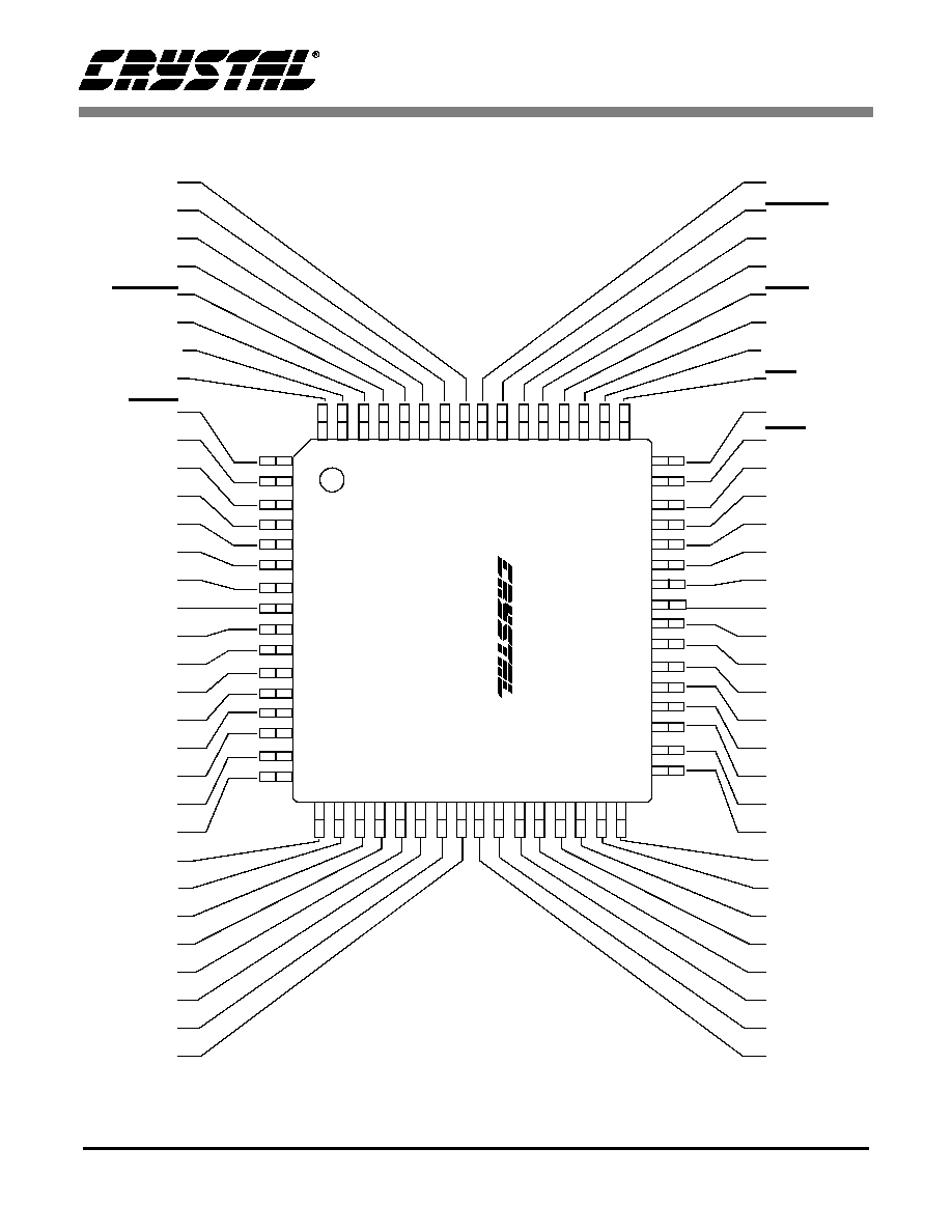
CS5376
DS256PP1
115
18. PIN DESCRIPTIONS
TIMEB
CLK
SYNC
SDDAT
SDRDY
SDCLK
SDTKO
SDTKI
TRST
TMS
TCK
TDI
TDO
GND
VD
TBSCLK
TBSDATA
NC
VDD2
MCLK/2
MCLK
MSYNC
MDATA4
MFLAG4
MDATA3
MFLAG3
MDATA2
MFLAG2
MDATA1
MFLAG1
GND
GND2
BOOT
RESET
VDD1
GND1
SINT
MOSI
MISO
SSI
SCK1
SSO
GPIO11:CS11
GPIO10:CS10
GPIO9:CS9
GPIO8:CS8
GPIO7
GPIO6
VD
GND
GND2
GPIO5
GPIO4:CS4
GPIO3:CS3
GPIO2:CS2
GPIO1:CS1
GPIO0:CS0
SCK2
SO
SI1
SI2
SI3
SI4
VDD2
1
2
3
4
5
6
7
8
9
10
11
12
13
14
15
16
17 18 19 20 21 22 23 2425 26 2728 29 30 3132
33
34
35
36
37
38
39
40
41
42
43
44
45
46
47
48
49
50
51
52
53
54
55
56
57
58
59
60
61
62
63
64
CS
53
76
64
-
P
IN T
Q
FP

CS5376
DS256PP1
116
Power Supply Connections
VDD1 - Positive Digital Power Supply, pin 54
Positive supply voltage for the communication interface. The communication interface includes
the JTAG pins (1, 2, 3, 4, 5), the serial data output pins (60, 61, 62, 63, 64), the serial port
interface 1 pins (47, 48, 49, 50, 51, 52), the GPIO 6-11 pins (41, 42, 43, 44, 45, 46), and
control signals RESET, BOOT, TIMEB, CLK, SYNC pins (55, 56, 57, 58, 59).
VDD2 - Positive Digitial Power Supply, pins 11, 25
Positive supply voltage for the modulator interface. The modulator interface includes the test
bit stream generator pins (8, 9), the modulator data output pins (12, 13, 14, 15, 16, 17, 18, 19,
20, 21, 22), the serial port interface 2 pins (26, 27, 28, 29, 30, 31), and the GPIO 0-5 pins (32,
33, 34, 35, 36, 37).
VD - Positive Digitial Power Supply, pins 7, 40
Positive supply voltages for the CS5376 logic core.
GND1, GND2, GND - Digital Ground, pin 53, 24, 38, 6, 23, 39
Reset Control
RESET - Reset, pin 55
Active low input. When low, the CS5376 is in a reset state.
BOOT - Boot mode selection, pin 56
Input signal sampled 1
µs after RESET is de-asserted. If low, the CS5376 boots in coprocessor
mode; if high, the CS5376 boots in stand-alone mode.
Clock and Synchronization
CLK - Clock Input, pin 58
Clock input, 32.768 MHz. All internal clocks, MCLK, MCLK/2, SPI 1 clock, SPI2 clock, and
TBSCLK are generated from CLK.
SYNC - Device Synchronization Input Signal, pin 59
Input synchronization signal. MSYNC is generated from a rising edge on this pin to
synchronize the modulators, sinc filter, and decimation engine.
TIMEB - Time Break, pin 57
Time Break input. Signals the Decimation Engine to set the time break (TB) flag in the output
status word for the sample representing the current sampling instant.

CS5376
DS256PP1
117
SPI 1 Interface
SSI - SPI 1 Slave Select Input, pin 49
Serial Peripheral Interface 1 slave select input pin. Shifting of data is performed as long as the
input slave select pin is low.
SCK1 - SPI 1 Clock, pin 48
Clock pin for the Serial Peripheral Interface 1 port. Maximum rate is 4 MHz.
MOSI - SPI 1 Master Out, Slave In, pin 51
Serial data output in master mode. Serial data input in slave mode.
MISO - SPI 1 Master Input, Slave Output, pin 50
Serial data input in master mode. Serial data output in slave mode.
SINT - SPI 1 Interrupt to Master, pin 52
Serial Peripheral Interface 1 interrupt. This is an active low pin with an open drain.
SSO - SPI 1 Slave Select Output, pin 47
Serial Peripheral Interface 1 slave select output pin.
SPI 2 Interface
SCK2 - SPI 2 Clock Output, pin 31
Output clock from the Serial Peripheral Interface 2 port. Maximum rate is 4 MHz.
SO - SPI 2 Data Output, pin 30
Serial Peripheral Interface 2 data output.
SI1 - SPI 2 Data Input 1, pin 29
Serial Peripheral Interface 2 data input 1.
SI2 - SPI 2 Data Input 2, pin 28
Serial Peripheral Interface 2 data input 2.
SI3 - SPI 2 Data Input 3, pin 27
Serial Peripheral Interface 2 data input 3.
SI4 - SPI 2 Data Input 4, pin 26
Serial Peripheral Interface 2 data input 4.

CS5376
DS256PP1
118
Modulator Interface
MCLK - Modulator Clock Output, pin 13
The CS5376 outputs a clock to operate the CS5372 modulator. The clock frequency is
selectable, nominal frequency 2.048 MHz.
MCLK/2 - Modulator Clock Divided by 2 Output, pin 12
The CS5376 outputs a slower clock to operate the CS5321 modulator. The clock frequency is
selectable, nominal frequency 1.024 MHz.
MSYNC - Modulator Sync Output, pin 14
A transition from logic low to high reinitializes the modulator timing to be synchronous with
the timing of the CS5376. Generated from the SYNC input signal.
MDATA[4:1] - Modulator Data Input, pin 15, 17, 19, 21
Modulator data is presented in a one-bit serial data stream (one's density) at a rate dictated by
the rate of the MCLK signal. 512 kbit and 256 kbit are typical MDATA rates.
MFLAG[4:1] - Modulator Flag Input, pin 16, 18, 20, 22
Logic input which transitions from low to high to indicate that the modulator is in an unstable
condition due to an over-ranged signal on its analog input.
Serial Data Output Port
SDTKI - Serial Data Chip Select Input, pin 64
Pulsed input signal which will initiate SDRDYZ signaling.
SDRDY - Serial Data Ready Output, pin 61
Signal which goes low to indicate that 32-bit conversion words are available to be clocked out
of the SDDAT pin.
SDCLK - Serial Data Clock Input, pin 62
Input clock which determines the rate at which the SDDAT bits are output.
SDDAT - Serial Data Output, pin 60
Serial data output for conversion words from the CS5376. Formatted to output a 32-bit digital
word consisting of one status byte followed by a three byte conversion word.
SDTKO - Serial Data Chip Select Output, pin 63
Output signal which indicates the current transaction has been completed.

CS5376
DS256PP1
119
Test Bit Stream Generator
TBSCLK - Test Signal Modulator Clock Output, pin 8
A dedicated clock output pin to interface with an external
- test DAC.
TBSDATA - Test Signal Modulator Data Output, pin 9
A dedicated data output pin to interface with an external
- test DAC.
GPIO
GPIO[11:0] - General Purpose Input/Output, pins 32 to 37, 41 to 46
General purpose pins for controlling local peripherals. Also used as chip selects for the SPI
ports.
JTAG / IEEE-1149.1 Test Access Port
TRST - Test Reset, pin 1
JTAG reset input pin, resets the test access port controller (TAP).
TMS - Test Mode Select, pin 2
JTAG mode select input pin, control signal to the test access port controller (TAP).
TCK - Test Clock, pin 3
JTAG clock input pin, clocks the test access port controller (TAP).
TDI - Test Data Input, pin 4
JTAG data input pin, the path by which serial data enters the device.
TDO - Test Data Output, pin 5
JTAG data output pin, the path by which serial data exits the device.

CS5376
DS256PP1
120
19. PACKAGE DIMENSIONS
INCHES
MILLIMETERS
DIM
MIN
MAX
MIN
MAX
A
---
0.063
---
1.60
A1
0.002
0.006
0.05
0.15
B
0.007
0.011
0.17
0.27
D
0.461
0.484
11.70
12.30
D1
0.390
0.398
9.90
10.10
E
0.461
0.484
11.70
12.30
E1
0.390
0.398
9.90
10.10
e*
0.016
0.024
0.40
0.60
L
0.018
0.030
0.45
0.75
µ
0.000°
7.000°
0.00°
7.00°
* Nominal pin pitch is 0.50 mm
Controlling dimension is mm.
JEDEC Designation: MS026
64L TQFP PACKAGE DRAWING
E1
E
D1
D
1
e
L
B
A1
A

· Notes ·
