Preliminary Product Information
This document contains information for a new product.
Cirrus Logic reserves the right to modify this product without notice.
1
Copyright
Cirrus Logic, Inc. 2001
(All Rights Reserved)
P.O. Box 17847, Austin, Texas 78760
(512) 445 7222 FAX: (512) 445 7581
http://www.cirrus.com
CS5371
/
CS5372
Low-Power High-Performance
Modulators
Features
l
Fourth-Order
Architecture
l
Clock Jitter Tolerant Architecture
l
Input Voltage Range 5 V
p-p
(2.5 V
diff
)
l
High Dynamic Range (SNR)
s
124 dB @ 411 Hz Bandwidth
s
121 dB @ 822 Hz Bandwidth
l
Low Total Harmonic Distortion (THD)
s
-118 dB Typical, -112 dB Maximum
l
Low Power Consumption
s
Normal Mode:
25 mW per Channel
s
Low Power Mode: 15 mW per Channel
l
Small Footprint 24 Pin SSOP Package
l
Single or Multi-Channel System Support
s
1 Channel System; CS5371
s
2 Channel System; CS5372
s
3 Channel System; CS5371 + CS5372
s
4 Channel System; CS5372 + CS5372
l
Single or Dual Power Supply Configurations
s
VA+ = +5 V;
VA- = 0 V;
VD = +3 V to +5 V
s
VA+ = +2.5 V; VA- = -2.5 V; VD = +3 V to +5 V
s
VA+ = +3 V;
VA- = -3 V;
VD = +3 V
Description
The CS5371 and CS5372 are one and two channel high
dynamic range, fourth-order
- modulators intended
for geophysical and sonar applications. Used in combi-
nation with the CS5376 digital filter, a unique high
resolution A/D measurement system results.
The CS5371 and CS5372 provide higher dynamic range
and lower total harmonic distortion than our industry
standard CS5321 modulator, while consuming signifi-
cantly less power per channel. The modulators generate
an oversampled serial bit stream at 512 kbits per second
when operated from a clock frequency of 2.048 MHz.
The CS5371 and CS5372 are available in a small 24-pin
SSOP package, providing exceptional performance in a
very small footprint.
In normal mode (LPWR = 0, MCLK = 2.048 MHz), power
consumption is 25 mW per channel, and in low power
mode (LPWR = 1, MCLK = 1.024MHz), power consump-
tion is 15 mW per channel. Each modulator can be
independently powered down to 1 mW per channel, and
by halting the input clock the modulators enter a mi-
cropower state using only 10 µW per channel.
ORDERING INFORMATION
CS5371 - BS -40
o
C to +85
o
C 24-pin SSOP
CS5372 - BS -40
o
C to +85
o
C 24-pin SSOP
DIA
W6
#
7+
ĂPS9@S
DIS
DIS
WS@A
WS@A
H96U6!
HT`I8
H8GF
QX9I
W9
-ĂHP9VG6UPS
DIA
QX9I!
DIA!
#
7+
ĂPS9@S
DIS!
DIS!
-ĂHP9VG6UPS
DIA!
PATU GQXS
9BI9
HAG6B!
8GP8F
B@I@S6UPS
H96U6
HAG6B
W6
DIA
W6
#
7+
ĂPS9@S
DIS
DIS
WS@A
WS@A
HT`I8
H8GF
QX9I
W9
-ĂHP9VG6UPS
DIA
PATU GQXS
9BI9
8GP8F
B@I@S6UPS
H96U6
HAG6B
W6
CS5371
CS5372
APR `01
DS255PP2

CS5371/CS5372
2
DS255PP2
TABLE OF CONTENTS
Contacting Cirrus Logic Support
For a complete listing of Direct Sales, Distributor, and Sales Representative contacts, visit the Cirrus Logic web site at:
http://www.cirrus.com/corporate/contacts/
Preliminary product information describes products which are in production, but for which full characterization data is not yet available. Advance product infor-
mation describes products which are in development and subject to development changes. Cirrus Logic, Inc. has made best efforts to ensure that the information
contained in this document is accurate and reliable. However, the information is subject to change without notice and is provided "AS IS" without warranty of
any kind (express or implied). No responsibility is assumed by Cirrus Logic, Inc. for the use of this information, nor for infringements of patents or other rights
of third parties. This document is the property of Cirrus Logic, Inc. and implies no license under patents, copyrights, trademarks, or trade secrets. No part of
this publication may be copied, reproduced, stored in a retrieval system, or transmitted, in any form or by any means (electronic, mechanical, photographic, or
otherwise) without the prior written consent of Cirrus Logic, Inc. Items from any Cirrus Logic website or disk may be printed for use by the user. However, no
part of the printout or electronic files may be copied, reproduced, stored in a retrieval system, or transmitted, in any form or by any means (electronic, mechanical,
photographic, or otherwise) without the prior written consent of Cirrus Logic, Inc.Furthermore, no part of this publication may be used as a basis for manufacture
or sale of any items without the prior written consent of Cirrus Logic, Inc. The names of products of Cirrus Logic, Inc. or other vendors and suppliers appearing
in this document may be trademarks or service marks of their respective owners which may be registered in some jurisdictions. A list of Cirrus Logic, Inc. trade-
marks and service marks can be found at http://www.cirrus.com.
1.
CHARACTERISTICS/SPECIFICATIONS....................................................... 4
ANALOG CHARACTERISTICS .................................................................. 4
5.0 AND 3.0 V DIGITAL CHARACTERISTICS ........................................... 6
ABSOLUTE MAXIMUM RATINGS ............................................................. 6
SWITCHING CHARACTERISTICS ............................................................ 7
2.
GENERAL DESCRIPTION. ........................................................................... 8
3.
MODULATOR PERFORMANCE.................................................................. 10
3.1.
Full Scale Signal Performance ......................................................... 10
3.2.
Noise Performance .......................................................................... 10
4.
SIGNAL INPUTS ......................................................................................... 10
4.1.
Differential Inputs - INR+/-, INF+/- ................................................... 10
4.2.
Anti-Alias Filters ............................................................................... 11
4.3.
Input Impedance .............................................................................. 11
4.4.
Maximum Signal Levels ................................................................... 12
5.
INPUT OFFSET ........................................................................................... 12
5.1.
Offset Enable - OFST....................................................................... 12
5.2.
Offset Drift ........................................................................................ 12
6.
VOLTAGE REFERENCE INPUTS .............................................................. 12
6.1.
Voltage Reference Configurations ................................................... 13
6.2.
VREF Input Impedance.................................................................... 13
6.3.
Gain Accuracy.................................................................................. 14
6.4.
Gain Drift .......................................................................................... 14
7.
DIGITAL FILTER INTERFACE .................................................................... 14
7.1.
Modulator Clock - MCLK .................................................................. 14
7.2.
Modulator Data - MDATA................................................................. 14
7.3.
Modulator Sync - MSYNC ................................................................ 15
7.4.
Modulator Flag - MFLAG.................................................................. 15
8.
POWER MODES ......................................................................................... 15
8.1.
Normal Power Mode ........................................................................ 15
8.2.
Low Power Mode - LPWR................................................................ 16
8.3.
Power Down Mode - PWDN............................................................. 16
8.4.
Micro Power Mode ........................................................................... 16
9.
POWER SUPPLY ........................................................................................ 16
9.1.
Power Supply Configurations........................................................... 16
9.2.
Power Supply Bypassing ................................................................. 16
9.3.
SCR Latch-up Considerations.......................................................... 16
9.4.
DC-DC Converter Considerations.................................................... 17
9.5.
Power Supply Rejection ................................................................... 17
10. PIN DESCRIPTION - CS5371 ..................................................................... 18
11. PIN DESCRIPTION - CS5372 ..................................................................... 20
12. PACKAGE DIMENSIONS ............................................................................ 22
CS5371/CS5372
DS255PP2
3
1. CHARACTERISTICS/SPECIFICATIONS
ANALOG CHARACTERISTICS
Notes:T
A
= -40 °C to +85 °C; VA+ = 2.5 V ± 5%; VA- = -2.5 V ± 5%;
VD = 3 V ± 5%; DGND = 0 V; MCLK = 2.048 MHz; LPWR = 0; VREF+/- = 2.5V (VREF- = -2.5 V; VREF+ = 0 V);
Devices are connected as shown in Figure 3, the System Connection Diagram, unless otherwise specified.
Notes: 1. Dynamic Range defined as 20log( (RMS full scale) / (RMS idle noise) )
2. Tested with full scale input signal of 31.25 Hz; OWR = 1000 sps; OFST = 0 or OFST = 1.
3. Characterized with input signals of 31.25 Hz and 52.63 Hz, each 6 dB down from full scale, OWR =
1000 sps.
4. Specification is for the parameter over the specified temperature range and is for the CS5371/CS5372
devices only and does not include the effects of external components.
5. Specifications are guaranteed by design and/or characterization.
6. The offset after calibration specification applies to the effective offset voltage for a full scale input to the
CS5371/CS5372 modulator, but is measured from the output digital codes from the CS5376.
7. The CS5371/CS5372 offset calibration is performed digitally and includes full scale range. Calibration
offsets greater than ± 5% of full scale will begin to subtract from the dynamic range.
Parameter
Symbol
CS5371-BS / CS5372-BS
Unit
Min Typ
Max
Specified Temperature Range
T
A
-40
-
+85
°C
Dynamic Performance
Dynamic Range
(Note 1)
OFST = 1
0 Hz to 1644 Hz
0 Hz to 822 Hz
0 Hz to 411 Hz
0 Hz to 206 Hz
0 Hz to 103 Hz
0 Hz to 51.5 Hz
0 Hz to 25.75 Hz
SNR
-
-
121
-
-
-
-
109
121
124
127
130
133
136
-
-
-
-
-
-
-
dB
dB
dB
dB
dB
dB
dB
Total Harmonic Distortion
(Note 2)
THD
-
-118
-112
dB
Intermodulation Distortion
(Note 3)
IMD
-
-115
-
dB
DC Accuracy
Channel to Channel Gain Variation
CGV
-
1
-
%
Full Scale Error
(Note 4)
FSE
-
1
-
%
Full Scale Drift
(Notes 4 and 5)
TC
FS
-
5
-
ppm/°C
Offset
(Notes 4)
V
ZSE
-
1
-
mV
Offset after Calibration
(Note 6)
-
±1
-
µV
Offset Calibration Range
(Note 7)
-
100
-
%F.S.
Offset Drift
(Notes 4 and 5)
TC
ZSE
-
1
-
µV/°C
CS5371/CS5372
4
DS255PP2
ANALOG CHARACTERISTICS
(Continued)
Notes: 8. The upper bandwidth limit is determined by the CS5376 digital filter. A simple single pole anti-alias filter
with a -3 dB frequency at (MCLK / 256) should be placed in front of each channel.
9. The input voltage range is for the configuration depicted in Figure 3, the System Connection Diagram,
and applies to signal frequencies from DC to the stop-band frequency selected in the CS5376.
10. Per channel. All outputs unloaded. All digital inputs forced to VD or GND respectively.
11. In Low Power Mode LPWR = 1, the Master Clock MCLK is reduced to 1.024 MHz. This reduces the
signal bandwidth by a factor of 2.
12. Tested with a 100 mVp-p sine wave applied separately to each supply.
Parameter
Symbol Min Typ
Max
Unit
Specified Temperature Range
T
A
-40
-
+85
°C
Input Characteristics
Input Signal Frequencies
(Note 8)
BW
DC
-
1644
Hz
Input Voltage Range
(Note 9)
VIN
-
-
5
V
p-p
Input Over-range Voltage Tolerance
(Note 9)
I
OVR
5
-
-
%F.S.
Input Signal plus Common Mode
VA-
-
VA+
V
Common Mode Rejection Ratio
CMRR
-
90
-
dB
Channel Crosstalk, CS5372 only
CXT
-
-120
-
dB
Voltage Reference Input
VREF
(VREF+) - (VREF-)
-
2.5
-
V
VREF Current
-
-
120
µA
Power Supplies
DC Power Supply Currents
(Note 10 and 11)
LPWR = 0; MCLK = 2.048 MHz
Analog
Digital
LPWR = 1; MCLK = 1.024 MHz
Analog
Digital
VA
VD
VA
VD
-
-
-
-
5.0
0.1
3.0
0.1
7.0
0.2
4.5
0.2
mA
mA
mA
mA
Power Down
CS5371
PWDN = 1
PWDN = 1, MCLK = 0
CS5372
PWDN1 or PWDN2 = 1
PWDN1 = PWDN2 = 1
PWDN1 = PWDN2 = 1; MCLK = 0
P
D
-
-
-
-
-
1
10
25
1
10
-
-
-
-
-
mW
µW
mW
mW
µW
Power Supply Rejection
DC - 128 kHz (Note 12)
PSRR
-
90
-
dB

CS5371/CS5372
DS255PP2
5
5.0 AND 3.0 V DIGITAL CHARACTERISTICS
Notes:T
A
= 25 °C; VA+, VD = 5 V ± 5% or 3 V ±
5%; AGND, DGND = 0 V; All voltages with respect to DGND.
ABSOLUTE MAXIMUM RATINGS
Notes:DGND = 0 V
Notes: 13. VA+ and VA- must satisfy {(VA+) - (VA-)} < +6.6 V.
14. VD and VA- must satisfy {(VD) - (VA-)} < +7.6 V.
15. Includes continuous over-voltage conditions at the analog input (AIN) pins.
16. Transient current of up to 100 mA can be safely tolerated without SCR latch-up.
17. Total power dissipation, including all input and output currents.
Parameter
Symbol Min Typ
Max
Unit
High-Level Input Voltage
V
IH
0.6 * VD
-
VD
V
Low-Level Input Voltage
V
IL
0.0
-
0.8
V
High-Level Output Voltage
I
out
= -5.0 mA
V
OH
(VD) - 1.0
-
-
V
Low-Level Output Voltage
I
out
= 5.0 mA
V
OL
-
-
0.4
V
Input Leakage Current
I
in
-
±1
±10
µA
3-State Leakage Current
I
OZ
-
-
±10
µA
Digital Output Pin Capacitance
C
out
-
9
-
pF
Parameter
Symbol Min Typ
Max
Unit
DC Power Supplies (Note 13 and 14)
Positive Digital
Positive Analog
Negative Analog
VD
VA+
VA-
-0.3
-0.3
+0.3
-
-
-
+6.0
+6.0
-3.3
V
V
V
Input Current, Any Pin Except Supplies
(Note 15 and 16)
I
IN
-
-
±10
mA
Input Current, Supplies
(Note 16)
I
IN
-
-
±50
mA
Output Current
I
OUT
-
-
±25
mA
Power Dissipation
(Note 17)
PDN
-
-
500
mW
Analog Input Voltage
All Analog Pins
V
INA
- 0.3
-
(VA+) + 0.3
V
Digital Input Voltage
All Digital Pins
V
IND
-0.3
-
(VD) + 0.3
V
Ambient Operating Temperature
T
A
-40
-
85
°C
Storage Temperature
T
stg
-65
-
150
°C

CS5371/CS5372
6
DS255PP2
SWITCHING CHARACTERISTICS
Notes:T
A
= -40 °C to +85 °C; VA+ = +2.5 V ± 5% VA- = -2.5 V ±
5%; VD = 3 V ± 5%; Inputs: Logic 0 = 0 V, Logic 1 = VD; C
L
= 50 pF
Notes: 18. If MCLK is removed, the CS5372 enters a micro power state.
19. Excludes MCLK input, MCLK should be driven with a signal having rise/fall times of 25 ns or faster.
20. MSYNC latched on MCLK falling edge, data output on next MCLK rising edge.
Parameter
Symbol Min Typ
Max
Unit
MCLK Frequency
(Note 18)
f
c
0.1
2.048
2.2
MHz
MCLK Duty Cycle
40
-
60
%
MCLK Jitter (In-band, Aliased in-band)
-
-
300
ps
MCLK Jitter (Out-of-band)
-
-
1
ns
Rise Times:
Any Digital Input
(Note 19)
Any Digital Output
t
risein
t
riseout
-
-
-
50
50
100
ns
ns
Fall Times:
Any Digital Input
(Note 19)
Any Digital Output
t
fallin
t
fallout
-
-
-
50
50
100
ns
ns
MSYNC Setup Time to MCLK falling
(Note 20)
t
mss
20
-
-
ns
MSYNC Hold Time after MCLK falling
t
msh
20
-
-
ns
MCLK rising to Valid MFLAG
t
mfh
-
35
65
ns
MCLK rising to Valid MDATA
t
mdv
-
60
90
ns
2.7 V
0.3 V
t
fallin
t
risein
2.7 V
0.3 V
t
riseout
t
fallout
Figure 1. Rise and Fall Times
MFLAG
MDATA
t mdv
t mdv
VALID DATA
VALID DATA
MCLK
t mss
MSYNC
t mfh
t msh
Figure 2. CS5372 Interface Timing

CS5371/CS5372
DS255PP2
7
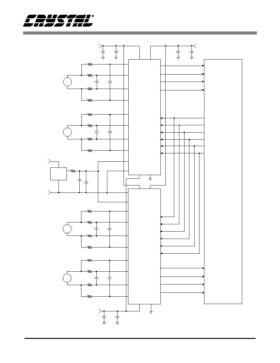
2. GENERAL DESCRIPTION
.
The CS5371 and CS5372 are one and two channel
fourth-order
- modulators, optimized for ex-
tremely high resolution measurement of signals be-
tween DC and 1644 Hz. They are designed to be
used with the CS5376 low power multi-channel
decimation filter. Figure 3 on page 8 shows a four-
channel system connection diagram for two
CS5372 and one CS5376.
High Performance
The CS5371/CS5372 modulators have exceptional
performance characteristics. Modulator dynamic
range (SNR) is 124 dB over a 411 Hz bandwidth,
with total harmonic distortion (THD) of -118 dB.
Low Power Consumption
The CS5371/CS5372 modulators have very low
power consumption. Power consumption is only
25 mW per channel in normal mode (LPWR=0,
MCLK=2.048 MHz), and 15 mW per channel in
low power mode (LPWR=1, MCLK=1.024 MHz).
An independently selectable power-down mode
(PWDN=1) can be used to disable a modulator and
reduces its power consumption to 1 mW. If MCLK
is then halted (MCLK=0), the modulator enters a
micropower state using only 10
µ
W per channel.
Small Package Size
The CS5371/CS5372 modulators are available in a
very small 24-pin SSOP package approximately
8 mm x 8 mm in size. The CS5372 has two modu-
lator channels per package to increase board layout
density even further.
Multi-Channel System Support
Combining the CS5371 and CS5372 modulators
with the CS5376 digital filter permits multiple
channel system configurations to be supported.
1 Channel - CS5371, CS5376
2 Channel - CS5372, CS5376
3 Channel - CS5371, CS5372, CS5376
4 Channel - CS5372, CS5372, CS5376
Differential Analog Signal Inputs
The CS5371/CS5372 modulators have differential
analog inputs capable of measuring signals up to
5.0 V peak-to-peak (2.5 V fully differential) when
using a 2.5 V voltage reference. The inputs will
tolerate a 5% over-range voltage and continue op-
erating at full specification.
Digital Filter Interface
The CS5371/CS5372 modulators are designed to
operate with the CS5376 digital filter. The CS5376
generates the modulator clock and synchronization
signal inputs (MCLK and MSYNC), while receiv-
ing the modulator data and over-range flag outputs
(MDATA and MFLAG). The modulators produce
an oversampled
- serial bit stream at 512 kbits
per second when operated from a 2.048 MHz mod-
ulator clock.
Multiple Power Supply Configurations
The CS5371/CS5372 modulators support multiple
power supply configurations. They can run from
single or dual supplies in the following configura-
tions:
s
VA+ = +5V;
VA- = 0V;
VD = +3V to +5V
s
VA+ = +2.5V; VA- = -2.5V;
VD = +3V to +5V
s
VA+ = +3V;
VA- = -3V;
VD = +3V
CS5371/CS5372
8
DS255PP2
CS5376
MSYNC
MSYNC
MFLAG1
M
FLAG1
MCLK
MCLK
MDATA1
MDATA1
MFLAG2
MFLAG2
MDATA2
MDATA2
0.01
µF
1 k
1 k
1 k
1 k
0.01
µF
INRI+
INFI+
INFI-
INRI-
INR2+
INF2+
INF2-
INR2-
INRI+
INFI+
INFI-
INRI-
INR2+
INF2+
INF2-
INR2-
~
MFLAG3
MFLAG1
MDATA3
MDATA1
MFLAG4
MFLAG2
MDATA4
MDATA2
OFST
LPWR
PWDN1
Channel 1
GPIO5
GPIO6
GPIO7
CS5372
CS5372
MSYNC
MCLK
OFST
LPWR
PWDN1
VA-
DGND
-3 V
+3 V
+3 V
VA+
VD+
VREF
+3 V
-3 V
VREF+
VREF-
VREF-
VREF+
VA+
VD+
VA-
DGND
PWDN2
GPIO4
PWDN2
X7R
COG
0.01µF
100 µF
220
0.01
µF
1 k
1 k
1 k
1 k
0.01
µF
~
Channel 2
COG
X7R
0.01
µF
1 k
1 k
1 k
1 k
0.01
µF
~
Channel 3
COG
X7R
0.01
µF
1 k
1 k
1 k
1 k
0.01
µF
~
Channel 4
COG
X7R
100 µF
0.01 µF
100 µF
0.01 µF
100 µF
0.01 µF
Figure 3. System Connection Diagram

CS5371/CS5372
DS255PP2
9
3. MODULATOR PERFORMANCE
Figures 4 and 5 illustrate the spectral performance
of the CS5371/CS5372 modulators when com-
bined with the CS5376 digital filter. The plots
were created from ten averaged 1024 point FFTs.
3.1.
Full Scale Signal Performance
Figure 4 illustrates the full-scale signal perfor-
mance of the CS5371/CS5372 modulators and
CS5376 digital filter using a 31.25 Hz input signal
and a 1000 sps output word rate. The outstanding
full-scale signal characteristics of the
CS5371/CS5372 modulators are shown, with no
harmonic components exceeding -120 dB. Analy-
sis of this data set yields a signal-to-noise ratio
(SNR) of 124.0 dB and a signal-to-distortion ratio
(SDR) of 119.0 dB. Note that the full-scale signal
peak in Figure 4 shows a slightly reduced ampli-
tude due to spectral smearing associated with the
FFT windowing function, and is a purely digital
phenomenon.
3.2.
Noise Performance
Figure 5 illustrates the noise performance of the
CS5371/CS5372 modulators and CS5376 digital
filter using a 31.25 Hz -24 dB input signal and a
1000 sps output word rate. The outstanding noise
characteristics of the CS5371/CS5372 modulators
are shown, with the averaged noise components
consistently below the -150 dB level. Analysis of
this data set yields a dynamic range of 124.7 dB.
Note that the 0.7 dB variation between the signal-
to-noise calculation in Figure 4 and the dynamic
range calculation in Figure 5 is not modulator de-
pendent and results from jitter in the test signal
generator when producing a full scale output, as ev-
idenced by the skirt surrounding the signal peak be-
low the -140 dB level in Figure 4.
4. SIGNAL INPUTS
The CS5371/CS5372 modulators use a switched
capacitor architecture for the analog signal inputs,
which has increased jitter tolerance relative to con-
tinuous time signal input stages.
4.1.
Differential Inputs - INR+/-, INF+/-
The analog signal inputs are differential and use
four pins: INR+, INR-, INF+, and INF-. The posi-
tive inputs, INR+ and INF+, are connected to the
positive half of the differential signal, while the
negative inputs, INR- and INF-, are connected to
Figure 4. 1024 Point FFT plot with a 31.25 Hz
input at Full Scale, ten averages
-200
-180
-160
-140
-120
-100
-80
-60
-40
-20
0
0
50
100
150
200
250
300
350
400
450
500
dB
Hz
S/N = 124.0 dB
S/D = 119.0 dB
-200
-180
-160
-140
-120
-100
-80
-60
-40
-20
0
0
50
100
150
200
250
300
350
400
450
500
dB
Hz
Dynamic Range = 124.7 dB
Figure 5. 1024 Point FFT plot with a 31.25 Hz
input at -24 dB, ten averages

CS5371/CS5372
10
DS255PP2
the negative half. The INR+ and INR- pins are
switched capacitor `rough charge' inputs for the
INF+ and INF- fine input pins.
The full scale analog signal span is defined by the
voltage applied across the VREF+ and VREF-
pins. A 2.5 volt reference input sets full scale sig-
nals as 5 volts peak-to-peak, or 2.5 volts fully dif-
ferential. Differential inputs increase the dynamic
range of small signals, reducing the gain require-
ments for input amplifier stages by a factor of two
relative to single ended analog inputs.
4.2.
Anti-Alias Filters
The CS5371/CS5372 modulator inputs must be
bandwidth limited to ensure modulator loop stabil-
ity and to prevent aliased high-frequency signals.
The modulators are 4th order and so are condition-
ally stable, and can be adversely affected by high
amplitude out-of-band signals. Also, aliasing ef-
fects degrade modulator performance if the analog
inputs are not bandwidth limited since out-of-band
signals can appear in the measurement bandwidth.
The use of a simple single pole low-pass anti-alias
filter on the differential inputs ensures out-of-band
signals are eliminated.
Anti-alias filtering may be accomplished actively
in an amplifier stage ahead of the CS5371/CS5372
modulator, or passively using an RC filter across
the differential rough and fine analog inputs. An
RC filter is recommended, even when using an am-
plifier stage, as it minimizes the `charge kick' that
the driving amplifier sees as switched capacitor
sampling is performed.
The -3 dB corner of the input anti-alias filter should
be set to the internal modulator sampling clock di-
vided by 64. The modulator sampling clock is a di-
vision by 4 of the modulator clock, MCLK. With
MCLK=2.048 MHz the modulator sampling clock
is 512 kHz, requiring an input filter with a -3 dB
corner at 8 kHz.
MCLK Frequency = 2.048 MHz
Sampling Frequency = MCLK / 4 = 512 kHz
-3 dB Filter Corner = Sample Freq / 64 = 8 kHz
RC filter = 8 kHz = 1 / [ 2
* (2 * R
diff
) * C
diff
]
It should be noted that when using low power mode
(LPWR=1 and MCLK=1.024 MHz) the modulator
sampling clock is 256 kHz, so the -3 dB filter cor-
ner should be scaled down to 4 kHz.
MCLK Frequency = 1.024 MHz
Sampling Frequency = MCLK / 4 = 256 kHz
-3 dB Filter Corner = Sample Freq / 64 = 4 kHz
RC filter = 4 kHz = 1 / [ 2
* (2 * R
diff
) * C
diff
]
Figure 3 illustrates the CS5372/CS5376 system
connections with input anti-alias filter components.
Filter components on the rough and fine pins
should be identical values for optimum perfor-
mance, with the capacitor values a minimum of
0.01
µF. The rough input can use either X7R or
C0G capacitors, while the fine input requires C0G
type capacitors for optimal linearity. Using X7R
capacitors on the fine inputs will degrade signal to
distortion performance up to 8 dB.
4.3.
Input Impedance
Due to the dynamic switched-capacitor input archi-
tecture the input current required from the analog
signal source, and thus the input impedance of the
analog input pins, changes any time MCLK is
changed. The input impedance of the rough charge
inputs, INR+ and INR-, is [1 / (f * C)] where f is the
modulator clock frequency, MCLK, and C is the in-
ternal sampling capacitor. A 2.048 MHz modula-
tor clock yields a rough input impedance of
approximately [1 / (2.048 MHz)*(20 pF)], or about
24 kohms.
Internal to the modulator the rough charge inputs
pre-charge the sampling capacitor used by the fine
inputs, therefore the effective input impedance of
the fine inputs is orders of magnitude above the im-
pedance of the rough inputs.

CS5371/CS5372
DS255PP2
11
4.4.
Maximum Signal Levels
The CS5371/CS5372 modulators are 4th order and
are therefore conditionally stable, and may go into
an oscillatory condition if the analog inputs over-
range beyond full scale by more than 5%. If an un-
stable condition is detected, the modulators col-
lapse to a 1st order system until loop stability is
achieved. During this time, the MFLAG pin tran-
sitions from low to high signaling the CS5376 dig-
ital filter to set an error bit in the digital output
word. The analog input signal must be reduced to
within the full scale range of the converter for at
least 32 MCLK cycles for the modulators to recov-
er from an unstable condition.
5. INPUT OFFSET
The CS5371/CS5372 modulators are
- type and
so can produce `idle tones' in the passband when
the input signal is a steady state DC signal within
about ±50 mV of the common mode input voltage.
Idle tones result from patterns in the output bit-
stream and appear in the measurement spectrum
about -135 dB down from full scale.
Idle tones can be eliminated by adding 100 mV or
more of differential DC offset to the modulator in-
puts. The added offset should be applied differen-
tially to the inputs, common mode offsets do not
affect idle tones.
5.1.
Offset Enable - OFST
If the analog inputs are within ±50 mV of the com-
mon mode voltage when no signal is present, the
OFST pin can be used to eliminate idle tones.
When OFST=1, +100 mV of differential offset is
added to the modulator analog inputs to push the
idle tones out of the measurement bandwidth. Care
should be taken that when OFST is active, offset
voltages generated by external circuitry do not ne-
gate the internally added offset.
5.2.
Offset Drift
Offset drift characteristics vary from part to part
and with changes in the power supply voltages. If
the CS5371/CS5372 is used in precision DC mea-
surement applications where offset drift is to be
minimized, the power supplies should be well reg-
ulated.
For the lowest offset drift, the CS5371/CS5372
modulators should operate with an MCLK of
2.048 MHz. The offset drift rate is inversely pro-
portional to clock frequency, with slower modula-
tor clock rates exhibiting more offset drift.
Operating from an MCLK of 1.024 MHz results in
twice the offset drift rate compared to an MCLK of
2.048 MHz.
Because offset drift is not linear with temperature,
an exact drift rate per °C cannot be specified. The
CS5371/CS5372 modulators will exhibit approxi-
mately 5 ppm/°C of offset drift operating with an
MCLK of 2.048 MHz.
6. VOLTAGE REFERENCE INPUTS
The CS5371/CS5372 modulators are designed to
operate with a 2.5 V voltage reference applied
across the VREF+ and VREF- pins to set the full
scale signal range of the analog inputs. A 2.5 V
voltage reference results in the highest dynamic
range and best signal-to-noise performance, though
smaller reference voltages may be used. When the
CS5371/CS5372 modulators are operated with a
2.5 V reference, the analog inputs measure full
scale signals of 5 volts peak-to-peak, or 2.5 volts
differential.
In a single supply power configuration the voltage
reference output should be connected to the
VREF+ pin with the VREF- pin connected to
ground. In a dual supply power configuration the
voltage reference should be powered from the VA+
and VA- supplies, with the modulator VREF+ pin
connected to the voltage reference output and the

CS5371/CS5372
12
DS255PP2
VREF- pin connected to VA-. Because most 2.5 V
voltage references require a power supply voltage
greater than 3 V to operate, when powering the
voltage reference from dual ±2.5 V or ±3.0 V sup-
plies the reference voltage into the VREF+ pin is
defined relative to the VA- supply.
The selected voltage reference should produce less
than 1
µVrms of noise in the measurement band-
width on the VREF+ pin. The CS5376 digital filter
output word rate selection determines the band-
width over which voltage reference noise affects
the CS5371/CS5372 modulator dynamic range.
6.1.
Voltage Reference Configurations
For a 2.5 V reference, the Linear Technology
LT1019-2.5 voltage reference yields low enough
noise if the output is filtered with a low pass RC fil-
ter as shown in Figure 6. The filtered version in
Figure 6 is acceptable for most spectral measure-
ment applications, but a buffered version with low-
er source impedance, Figure 7, may be preferred
for DC measurement applications. The configura-
tion shown in Figure 7 can use a Linear Technolo-
gy LT1077 or similar low voltage op-amp to buffer
the voltage reference output.
6.2.
VREF Input Impedance
Due to the dynamic switched-capacitor input archi-
tecture the input current required from the voltage
reference, and thus the input impedance of the
modulator VREF+ pin, will change any time
MCLK is changed. The input impedance of the
voltage reference input is calculated similar to the
analog signal input impedance as [1 / (f * C)]
where f is the modulator clock frequency, MCLK,
200
To VREF+
Option A
To VREF -
0.1
µF
68
µF
+
+3 V
2.5 REF
0.1
µF
10
µF
-3 V
0.1
µF
10
µF
Figure 6. 2.5 Voltage Reference Option A
+
-
49.9
1k
100
1k
10k
100
µF
AL
+
+
To VREF+
Option B
AL
OPAMP
To VREF -
0.1
µF
68
µF
Tant
+
100
µF
+3 V
2.5 REF
0.1
µF
10
µu
-3 V
0.1
µF
10
µu
Figure 7. 2.5 Voltage Reference Option B

CS5371/CS5372
DS255PP2
13
and C is the internal sampling capacitor. A
2.048 MHz MCLK yields a voltage reference input
impedance of approximately
[1 / (2.048 MHz)*(20 pF)], or about 24 kohms.
6.3.
Gain Accuracy
Gain accuracy of the CS5371/CS5372 modulators
is affected by variation of the voltage reference in-
put. A change in the voltage reference input im-
pedance due to a change in MCLK could affect
gain accuracy when using the higher source imped-
ance configuration of Figure 6. The VREF+ pin in-
put impedance and the external low-pass filter
resistor create a resistive voltage divider for the
output reference voltage, reducing the effective
voltage reference input. If gain error is to be mini-
mized, especially when MCLK is to be changed,
the voltage reference should have a low output im-
pedance to minimize the effect of the resistive volt-
age divider. The buffered voltage reference
configuration of Figure 7 offers lower output im-
pedance and more stable gain characteristics.
6.4.
Gain Drift
Gain drift of the CS5371/CS5372 modulators due
to temperature is around 5 ppm/°C, and does not in-
clude the temperature drift characteristics of the ex-
ternal voltage reference. Gain drift is not affected
by the modulator sample rate or by power supply
variations.
7. DIGITAL FILTER INTERFACE
The CS5371/CS5372 modulators are designed to
operate with the CS5376 digital filter. The CS5376
generates the modulator clock and synchronization
signal inputs (MCLK and MSYNC), while receiv-
ing the modulator data and over-range flag outputs
(MDATA and MFLAG). The modulators produce
an oversampled
- serial bit stream at 512 kbits
per second when operated from a 2.048 MHz mod-
ulator clock.
7.1.
Modulator Clock - MCLK
For proper operation, the CS5371/CS5372 modula-
tors must be provided with a CMOS compatible
clock on the MCLK pin. MCLK is internally divid-
ed by four to generate the modulator sampling
clock. MCLK must have less than 300 ps of in-
band jitter to maintain full performance specifica-
tions.
When used with the CS5376 digital filter, MCLK is
automatically generated and is typically
2.048 MHz or 1.024 MHz. MCLK can be generat-
ed by other means, using a crystal oscillator for ex-
ample, and can run any rate between 100 kHz and
2.2 MHz. If MCLK is disabled, the modulators are
placed into a micro-power state. They are
equipped with loss of clock detection circuitry to
force power down if MCLK is removed.
The choice of MCLK frequency affects the perfor-
mance of the CS5371/CS5372 modulators. They
exhibit the best dynamic range (SNR) performance
with faster MCLK rates because of increased over-
sampling of the analog input signal. The modula-
tors exhibit the best total harmonic distortion
(THD) performance with slower MCLK rates be-
cause slower sampling allows more time to settle
the analog input signal.
7.2.
Modulator Data - MDATA
The CS5371/CS5372 modulators output a
- se-
rial bitstream to the MDATA pin, with a one's den-
sity proportional to the amplitude of the analog
input signal and a bit rate determined by the modu-
lator sampling clock. The modulator sampling
clock is a divide by four of MCLK, so for a
2.048 MHz MCLK the modulator sampling clock
and MDATA output bit rate will be 512 kHz.
The MDATA output has a one's density defined as
nominal 50% for no signal input, 86% for positive
full scale, and 14% for negative full scale. It has a
maximum positive over-range capability to 93%
and a maximum negative over-range capability to

CS5371/CS5372
14
DS255PP2
7%. The one's density of the MDATA output is de-
fined as the ratio of `1' bits to total bits in the serial
bitstream output, i.e. an 86% one's density has, on
average, a `1' value in 86 of every 100 output data
bits.
When operated with the CS5376 digital filter, the
full scale 24-bit output codes range from
0x5FFFFF (decimal 6,291,455) to 0xA00001 (dec-
imal -6,291,455).
Note that for a full scale input signal, 5 V
p-p
(2.5 V
diff
) with VREF=2.5 V, the CS5371/CS5372
and CS5376 chip set does not output a maximum
24-bit 2's complement digital code of 0x7FFFFF
(digital 8,388,607), but instead a lower scaled value
to allow over-range capability. The CS5376 con-
verts to full performance specification up to a pos-
itive over-range value of 0x64CCCC (decimal
6,606,028) and down to a negative over-range val-
ue of 0x9B3334 (decimal -6,606,028).
7.3.
Modulator Sync - MSYNC
To synchronize the analog sampling instant and
timing of the digital output bitstream, the
CS5371/CS5372 modulators use an MSYNC sig-
nal. When using the CS5376 digital filter, MSYNC
is automatically generated from a SYNC signal in-
put from the external system.
The MSYNC input is rising edge triggered and re-
sets the internal MCLK counter-divider so the ana-
log sampling instant occurs during a consistent
MCLK phase. It also sets the MDATA output tim-
ing so the bitstream can be properly sampled by the
CS5376 digital filter input.
7.4.
Modulator Flag - MFLAG
The CS5371/CS5372 modulators are 4th order
-
and are therefore conditionally stable. The mod-
ulators may go into an oscillatory condition if the
analog inputs are over-ranged more than 5% past
either positive or negative full scale.
If an unstable condition is detected, the modulators
collapse to a 1st order system until loop stability is
achieved. During this time, the MFLAG pin tran-
sitions from low to high to signal an error condi-
tion. The analog input signal must be reduced to
within the full scale range for at least 32 MCLK cy-
cles for the modulator to recover from an unstable
condition.
The MFLAG output connects to a dedicated input
on the CS5376 digital filter, causing an error bit to
be set in the status portion of the digital output data
word when detected.
8. POWER MODES
Four power modes are available when using the
CS5371/CS5372 modulators. Normal power and
low power modes are operational modes, power
down and micro power modes are non-operational
standby modes.
8.1.
Normal Power Mode
The normal operational mode for the modulators,
LPWR=0 and MCLK=2.048 MHz, provides the
best performance with power consumption of
25 mW per channel. This power mode is recom-
mended when maximum conversion accuracy is re-
quired.
Table 1. Output coding for the CS5371/CS5372 and
CS5376 combination
Modulator Input
Signal
CS5376 Filter
Output Code
HEX
Decimal
> + (VREF + 5%)
Error Flag Possible
+ (VREF + 5%)
64CCCC
+6606028
+VREF
5FFFFF
+6291455
0V
000000
0
-VREF
A00001
-6291455
- (VREF + 5%)
9B3334
-6606028
> - (VREF + 5%)
Error Flag Possible

CS5371/CS5372
DS255PP2
15
8.2.
Low Power Mode - LPWR
The modulators have a low-power operational
mode, LPWR=1 and MCLK=1.024 MHz, that re-
duces power consumption to 15 mW per channel at
the expense of 3 dB of dynamic range. This oper-
ational mode is recommended when minimizing
power is more important than maximizing dynamic
range.
When operated with LPWR=1, the modulator sam-
pling clock (MCLK / 4) must be restricted to rates
of 256 kHz or less, which requires MCLK to run at
1.024 MHz or less. Operating in low power mode
with modulator sample rates greater than 256 kHz
will significantly degrade total harmonic distortion
performance.
8.3.
Power Down Mode - PWDN
The modulators have a power down mode,
PWDN=1 and MCLK=Active, that disables the op-
eration of the selected modulator channel and re-
duces its power consumption to 1 mW. Each
modulator has an independent power down pin,
PWDN on the CS5371 and PWDN1, PWDN2 on
the CS5372. Note that when the modulators are
powered down and MCLK is active, the internal
clock generator is still drawing minimal currents.
8.4.
Micro Power Mode
Standby power consumption of the modulators can
be minimized by placing them into a micro power
mode, PWDN=1 and MCLK=0. Micro power
mode requires setting the PWDN pin and halting
MCLK to remove the clock generator input current.
Micro power mode consumes only 10 µW of pow-
er.
9. POWER SUPPLY
The CS5371/CS5372 modulators have one positive
analog power supply pin, VA+, one negative ana-
log power supply pin, VA-, one digital power sup-
ply pin, VD, and one digital ground pin, DGND.
The analog and digital circuitry is separated inter-
nally to enhance performance, therefore power
must be supplied to all three supply pins and the
digital ground pin must be referenced to system
ground.
9.1.
Power Supply Configurations
The CS5371/CS5372 analog supplies can be pow-
ered by a single +5 V supply and analog ground, or
by dual supplies of + 2.5 V or + 3.0 V. When using
dual supplies, the positive and negative analog
power supplies must be equivalent in voltage but
opposite in polarity and must satisfy the following
conditions:
(VA+) - (VA-) < 6.6 volts
(VD) - (VA-) < 7.6 volts
These conditions permit several power supply con-
figurations.
s
VA+ = +5 V;VA- = 0 V;VD+ = +3 V to +5 V
s
VA+ = +2.5 V;VA- = -2.5 V;VD+ = +3 V to +5 V
s
VA+ = +3 V;VA- = -3 V;VD+ = +3 V
When used with the CS5376 digital filter the max-
imum voltage differential between the modulator
digital supply, VD, and the CS5376 digital supply,
VDD2, must be less than 0.3 V.
9.2.
Power Supply Bypassing
The analog and digital supply pins, VA+, VA-, and
VD, should be decoupled to system ground with
0.01
µF and 10 µF capacitors, or with a single
0.1
µF capacitor. Bypass capacitors can be X7R,
tantalum, or any other dielectric types.
9.3.
SCR Latch-up Considerations
The VA- pin is tied to the CS5371/CS5372 sub-
strate and should always be connected to the most
negative supply voltage to ensure SCR latch-up
does not occur. In general, latch-up may occur
when any pin voltage is 0.7 V or more below VA-.

CS5371/CS5372
16
DS255PP2
When using dual power supplies, it is recommend-
ed to connect the VA- analog supply pin to system
ground using a reversed biased Schottky diode.
This configuration clamps the VA- pin a maximum
of 0.3 V above ground to ensure SCR latch-up does
not occur during power up. If the VA+ supply
ramps before the VA- supply, the VA- pin can be
pulled above ground through the CS5371/CS5372.
If the VA- supply pin is unintentionally pulled
0.7 V above the DGND pin, SCR latch-up can oc-
cur.
9.4.
DC-DC Converter Considerations
Many measurement systems are battery powered
and utilize DC-DC converters to generate the nec-
essary supply voltages for the system. To mini-
mize the effects of interference, it is desirable to
operate the DC-DC converter at a frequency which
is rejected by the digital filter, or else synchronous-
ly to the modulator sample clock rate. A synchro-
nous DC-DC converter whose operating frequency
is derived from MCLK minimizes the potential for
`beat frequencies' appearing in the
measurement
band.
9.5.
Power Supply Rejection
Power supply rejection of the CS5371/CS5372
modulators is frequency dependent. The CS5376
digital filter rejects power supply noise for frequen-
cies above the filter corner frequency. For frequen-
cies between DC and the digital filter corner
frequency, power supply rejection is nearly con-
stant at 90 dB.

CS5371/CS5372
DS255PP2
17
10. PIN DESCRIPTION - CS5371
Power Supplies
VA+
_
Positive Analog Power Supply, pin 8
Positive supply voltage.
VA-
_
Negative Analog Power Supply, pin 7
Negative supply voltage.
VD
_
Positive Digital Power Supply, pin 13, 18
Positive supply voltage.
DGND
_
Digital Ground, pin 17
Analog Inputs
INR+
_
Rough Non-Inverting Input, pin 1
Rough non-inverting analog input. The rough input settles non-linear currents to improve
linearity on the fine input and reduce harmonic distortion.
INR-
_
Rough Inverting Input, pin 4
Rough inverting analog input. The rough input settles non-linear currents to improve linearity
on the fine input and reduce harmonic distortion.
INF+
_
Fine Non-Inverting Input, pin 2
Fine non-inverting analog input.
1
2
3
4
5
6
7
8
17
18
19
20
21
22
23
24
9
10
11
12
13
14
15
16
Rough Non-Inverting Input
INR+
Fine Non-Inverting Input
INF+
Fine Inverting Input
INF-
Rough Inverting Input
INR-
Positive Voltage Reference Input
VREF+
Negative Voltage Reference Input
VREF-
Negative Analog Power Supply
VA-
Positive Analog Power Supply
VA+
No Internal Connection
NC
No Internal Connection
NC
No Internal Connection
NC
No Internal Connection
NC
PWDN
Power-down Enable
LPWR
Low Power Mode Select
MFLAG
Modulator Flag Output
MDATA
Modulator Data Output
MSYNC
Modulator Sync Input
MCLK
Modulator Clock Input
VD
Positive Digital Power Supply
DGND
Digital Ground
NC
No Internal Connection
NC
No Internal Connection
OFST
Offset Mode Select
VD
Positive Digital Power Supply

CS5371/CS5372
18
DS255PP2
INF-
_
Fine Inverting Input, pin 3
Fine inverting analog input.
VREF+
_
Positive Voltage Reference Input, pin 5
Input for an external +2.5 V voltage reference relative to VREF-.
VREF-
_
Negative Voltage Reference Input, pin 6
This pin must be tied to VA-.
Digital Inputs
MCLK
_
Modulator Clock Input, pin 19
A CMOS compatible clock input for the modulator internal master clock, nominally 2.048
MHz with an amplitude equal to the VD digital power supply.
MSYNC
_
Modulator Sync Input, pin 20
A low to high transition resets the internal clock phasing of the modulator. This assures the
sampling instant and modulator data output are synchronous to the external system.
OFST
_
Offset Mode Select, pin 14
When high, adds approximately +100mV of offset to the analog inputs to guarantee any zero
input
- idle tones are removed. When low, no offset is added.
LPWR
_
Low Power Mode Select, pin 23
When set high with MCLK operating at 1.024 MHz, modulator power dissipation is reduced to
15 mW per channel.
PWDN
_
Power-down Mode, pin 24
When high, the modulator is in power down mode and consumes 1mW. Halting MCLK while
in power down mode reduces modulator power dissipation to 10
µW
.
Digital Outputs
MDATA
_
Modulator Data Output, pin 21
Modulator data is output as a 1-bit serial data stream at a 512 kHz rate with an MCLK input of
2.048 MHz. Modulator data is output at a 256 kHz rate with an MCLK input of 1.024 MHz.
MFLAG
_
Modulator Flag Output, pin 22
A high level output indicates the modulator is unstable due to an over-range on the analog
inputs.
CS5371/CS5372
DS255PP2
19
11. PIN DESCRIPTION - CS5372
Power Supplies
VA+
_
Positive Analog Power Supply, pin 8
Positive supply voltage.
VA-
_
Negative Analog Power Supply, pin 7
Negative supply voltage.
VD
_
Positive Digital Power Supply, pin 18
Positive supply voltage.
DGND
_
Digital Ground, pin 17
Analog Inputs
INR1+, INR2+
_
Channel 1 & 2 Rough Non-Inverting Inputs, pin 1, 12
Rough non-inverting analog inputs. The rough inputs settle non-linear currents to improve
linearity on the fine inputs and reduce harmonic distortion.
INR1-, INR2-
_
Channel 1 & 2 Rough Inverting Inputs, pin 4, 9
Rough inverting analog inputs. The rough inputs settle non-linear currents to improve linearity
on the fine inputs and reduce harmonic distortion.
INF1+, INF2+
_
Channel 1 & 2 Fine Non-Inverting Input, pin 2, 11
Fine non-inverting analog inputs.
1
2
3
4
5
6
7
8
17
18
19
20
21
22
23
24
9
10
11
12
13
14
15
16
Ch. 1 Rough Non-Inverting Input
INR1+
Ch. 1 Fine Non-Inverting Input
INF1+
Ch. 1 Fine Inverting Input
INF1-
Ch. 1 Rough Inverting Input
INR1-
Positive Voltage Reference Input
VREF+
Negative Voltage Reference Input
VREF-
Negative Analog Power Supply
VA-
Positive Analog Power Supply
VA+
Ch. 2 Rough Inverting Input
INR2-
Ch. 2 Fine Inverting Input
INF2-
Ch. 2 Fine Non-Inverting Input
INF2+
Ch. 2 Rough Non-Inverting Input
INR2+
PWDN1
Ch. 1 Power-down Enable
LPWR
Low Power Mode Select
MFLAG1
Ch. 1 Modulator Flag Output
MDATA1
Ch. 1 Modulator Data Output
MSYNC
Modulator Sync Input
MCLK
Modulator Clock Input
VD
Positive Digital Power Supply
DGND
Digital Ground
MDATA2
Ch. 2 Modulator Data Output
MFLAG2
Ch. 2 Modulator Flag Output
OFST
Offset Mode Select
PWDN2
Ch. 2 Power-down Enable

CS5371/CS5372
20
DS255PP2
INF1-, INF2-
_
Channel 1 & 2 Fine Inverting Input, pin 3, 10
Fine inverting analog inputs.
VREF+
_
Positive Voltage Reference Input, pin 5
Input for an external +2.5V voltage reference relative to VREF-.
VREF-
_
Negative Voltage Reference Input, pin 6
This pin must be tied to VA-.
Digital Inputs
MCLK
_
Modulator Clock Input, pin 19
A CMOS compatible clock input for the modulator internal master clock, nominally 2.048
MHz with an amplitude equal to the VD digital power supply.
MSYNC
_
Modulator Sync Input, pin 20
A low to high transition resets the internal clock phasing of the modulator. This assures the
sampling instant and modulator data output are synchronous to the external system.
OFST
_
Offset Mode Select, pin 14
When high, adds approximately +100mV of offset to the analog inputs to guarantee any zero
input
- idle tones are removed. When low, no offset is added.
LPWR
_
Low Power Mode Select, pin 23
When set high with MCLK operating at 1.024 MHz, modulator power dissipation is reduced to
15 mW per channel.
PWDN1, PWDN2
_
Channel 1 & 2 Power-down Mode, pin 24, 13
When high, the modulator is in power down mode and consumes 1mW. Halting MCLK while
in power down mode reduces modulator power dissipation to 10
µW
.
Digital Outputs
MDATA1, MDATA2
_
Modulator Data Output, pin 21, 16
Modulator data is output as a 1-bit serial data stream at a 512 kHz rate with an MCLK input of
2.048 MHz. Modulator data is output at a 256 kHz rate with an MCLK input of 1.024 MHz.
MFLAG1, MFLAG2
_
Modulator Flag, pin 22, 15
A high level output indicates the modulator is unstable due to an over-range on the analog
inputs.

CS5371/CS5372
DS255PP2
21
12. PACKAGE DIMENSIONS
Notes: 1. "D" and "E1" are reference datums and do not included mold flash or protrusions, but do include mold
mismatch and are measured at the parting line, mold flash or protrusions shall not exceed 0.20 mm per
side.
2. Dimension "b" does not include dambar protrusion/intrusion. Allowable dambar protrusion shall be
0.13 mm total in excess of "b" dimension at maximum material condition. Dambar intrusion shall not
reduce dimension "b" by more than 0.07 mm at least material condition.
3. These dimensions apply to the flat section of the lead between 0.10 and 0.25 mm from lead tips.
INCHES
MILLIMETERS
NOTE
DIM
MIN
MAX
MIN
MAX
A
--
0.084
--
2.13
A1
0.002
0.010
0.05
0.25
A2
0.064
0.074
1.62
1.88
b
0.009
0.015
0.22
0.38
2,3
D
0.311
0.335
7.90
8.50
1
E
0.291
0.323
7.40
8.20
E1
0.197
0.220
5.00
5.60
1
e
0.024
0.027
0.61
0.69
L
0.025
0.040
0.63
1.03
0°
8°
0°
8°
24 PIN SSOP PACKAGE DRAWING
E
N
1 2 3
e
b
2
A1
A2
A
D
SEATING
PLANE
E1
1
L
SIDE VIEW
END VIEW
TOP VIEW