PHOTOCOUPLER
PS9113
1 Mbps, OPEN COLLECTOR OUTPUT
HIGH CMR, INTELLIGENT POWER MODULE
5-PIN SOP PHOTOCOUPLER
-
NEPOC Series
-
DESCRIPTION
The PS9113 is an optically coupled isolator containing a GaAlAs LED on the input side and a photo diode and a
signal processing circuit on the output side on one chip.
The PS9113 is specified high CMR, high CTR and pulse width distortion with operating temperature. It is suitable
for IPM drive.
FEATURES
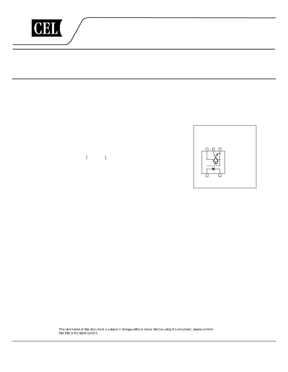
PIN CONNECTION
(Top View)
5
3
4
1. Anode
2. Cathode
3. GND
4. V
O
5. V
CC
1
2
� High instantaneous common mode rejection voltage (CM
H
, CM
L
=
�
15 kV/
�
s MIN.)
� Small package (5-pin SOP)
� High-speed response (t
PHL
= 500 ns MAX., t
PLH
= 750 ns MAX.)
� Maximum propagation delays (t
PLH
-
t
PHL
= 270 ns TYP.)
� Pulse width distortion ( t
PHL
-
t
PLH
= 270 ns TYP.)
� Ordering number of taping product: PS9113-F3, F4: 2 500 pcs/reel
� Pb-Free
product
� Safety
standards
� UL approved: File No. E72422
� DIN EN60747-5-2 (VDE0884 Part2) approved: No. 40008902 (Option)
APPLICATIONS
� IPM
Driver
� General purpose inverter
Document No. PN10265EJ03V0DS (3rd edition)
Date Published August 2005 CP(K)
The mark shows major revised points.
PS9113
PACKAGE DIMENSIONS (UNIT: mm)
1.27
0.4
+0.10
�0.05
0.25 M
0.1�0.1
2.6�0.2
4.4
7.0�0.3
0.5�0.3
0.15
+0.10 �0.05
3.4
+0.3
�0.1
FUNCTIONAL DIAGRAM
5
4
3
1
2
LED
Output
ON
L
OFF
H
Shield
Data Sheet PN10265EJ03V0DS
2
PS9113
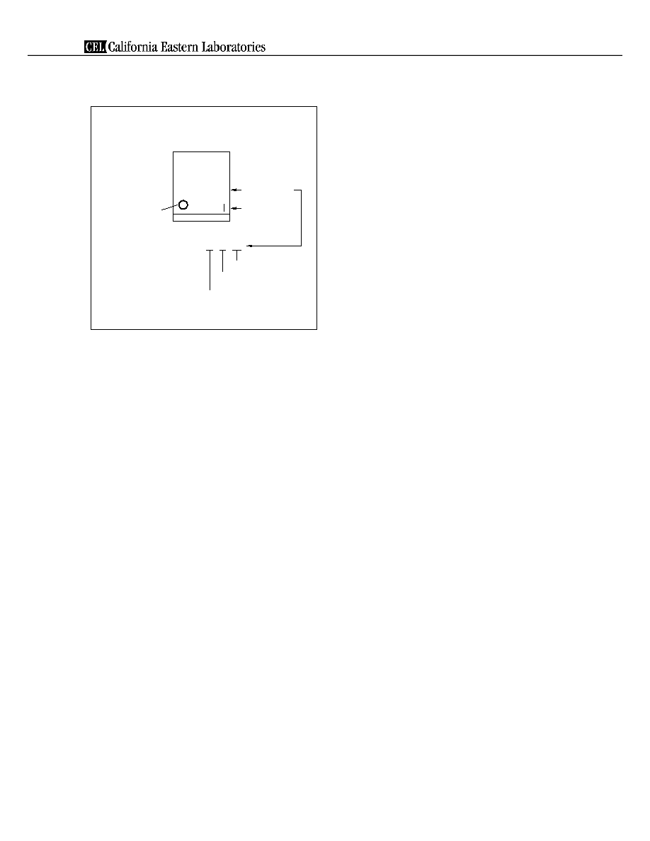
MARKING EXAMPLE
No. 1 pin Mark
Initial of NEC
(Engraved mark)
Rank Code
Year Assembled
(Last 1 Digit)
Week Assembled
N
2
34
Assembly Lot
9113
N234
N
*1
*1 Bar : Pb-Free
Data Sheet PN10265EJ03V0DS
3

PS9113
ORDERING INFORMATION
Part Number
Order Number
Solder Plating
Specification
Packing Style
Safety Standard
Approval
Application
Part
Number
*1
PS9113
PS9113-A
Pb-Free
20 pcs (Tape 20 pcs cut)
Standard products
PS9113
PS9113-F3
PS9113-F3-A
Embossed Tape 2500 pcs/reel
(UL approved)
PS9113-F4 PS9113-F4-A
PS9113-V
PS9113-V-A
20 pcs (Tape 20 pcs cut)
DIN EN60747-5-2
PS9113-V-F3
PS9113-V-F3-A
Embossed Tape 2 500 pcs/reel (VDE0884 Part2)
PS9113-V-F4 PS9113-V-F4-A
Approved
(Option)
*1 For the application of the Safety Standard, following part number should be used.
ABSOLUTE MAXIMUM RATINGS (T
A
= 25
�
C, unless otherwise specified)
Parameter Symbol
Ratings
Unit
Diode Forward
Current
*1
I
F
25 mA
Reverse
Voltage
V
R
5 V
Detector Supply Voltage
V
CC
-
0.5 to +35
V
Output
Voltage
V
O
-
0.5 to +35
V
Output
Current
I
O
15 mA
Power
Dissipation
*2
P
C
100 mW
Isolation Voltage
*3
BV 2
500
Vr.m.s.
Operating Ambient Temperature
T
A
-
40 to +100
�
C
Storage Temperature
T
stg
-
55 to +125
�
C
*1 Reduced to 0.33 mA/
�
C at T
A
= 70
�
C or more.
*2 Reduced to 1.9 mW/
�
C at T
A
= 70
�
C or more.
*3 AC voltage for 1 minute at T
A
= 25
�
C, RH = 60% between input and output.
Pins 1-2 shorted together, 3-5 shorted together.
RECOMMENDED OPERATING CONDITIONS
Parameter Symbol
MIN.
TYP.
MAX.
Unit
High Level Input Current
I
FH
10 20 mA
Output Voltage
V
O
0 30 V
Supply Voltage
V
CC
4.5 30 V
LED Off Voltage
V
F
0 0.8 V
Data Sheet PN10265EJ03V0DS
4
PS9113
ELECTRICAL CHARACTERISTICS (T
A
=
-
40 to +100
�
C, V
CC
= 15 V, unless otherwise specified)
Parameter Symbol Conditions MIN.
TYP.
*1
MAX. Unit
Diode Forward
Voltage
V
F
I
F
= 10 mA
1.3
1.65
2.1
V
Reverse
Current
I
R
V
R
= 3 V
200
�
A
Terminal
Capacitance C
t
V = 0 V, f = 1 MHz, T
A
= 25
�
C
30
pF
Detector Low Level Output Voltage
V
OL
I
F
= 10 mA, I
OL
= 2.4 mA
0.13
0.6
V
High Level Output Current
I
OH
V
CC
= V
O
= 30 V, V
F
= 0.8 V
0.01
50
�
A
High Level Supply Current
I
CCH
V
CC
= 30 V, V
F
= 0.8 V, V
O
= open
0.6
1.3
mA
Low Level Supply Current
I
CCL
V
CC
= 30 V, I
F
= 10 mA, V
O
= open
0.6
1.3
mA
Coupled Threshold Input Current
(H
L)
I
FHL
V
O
= 0.8 V, I
O
= 0.75 mA
1.5
5.0
mA
Current Transfer Ratio (I
C
/I
F
) CTR I
F
= 10 mA, V
O
= 0.6 V
44
110
%
Isolation
Resistance R
I-O
V
I-O
= 1 kV
DC
, RH = 40 to 60%,
T
A
= 25
�
C
10
11
Isolation
Capacitance C
I-O
V = 0 V, f = 1 MHz, T
A
= 25
�
C
0.6 pF
Propagation Delay Time
(H
L)
*2
t
PHL
I
F
= 10 mA, R
L
= 20 k
, C
L
= 100 pF,
V
THHL
= 1.5 V, V
THLH
= 2.0 V
250
500 ns
Propagation Delay Time
(L
H)
*2
t
PLH
520
750
Maximum
Propagation
Delays
t
PLH
-
t
PHL
-
200 270 650
Pulse Width Distortion
(PWD)
*2
t
PHL-
t
PLH
270
650
Common Mode
Transient Immunity at High
Level Output
*3
CM
H
T
A
= 25
�
C, I
F
= 0 mA, V
O
> 3.0 V,
V
CM
= 1.5 kV, R
L
= 20 k
,
C
L
= 100 pF
15
kV/
�
s
Common Mode
Transient Immunity at Low
Level Output
*3
CM
L
T
A
= 25
�
C, I
F
= 10 mA, V
O
< 1.0 V,
V
CM
= 1.5 kV, R
L
= 20 k
,
C
L
= 100 pF
15
kV/
�
s
Data Sheet PN10265EJ03V0DS
5
PS9113
*1 Typical values at T
A
= 25
�
C.
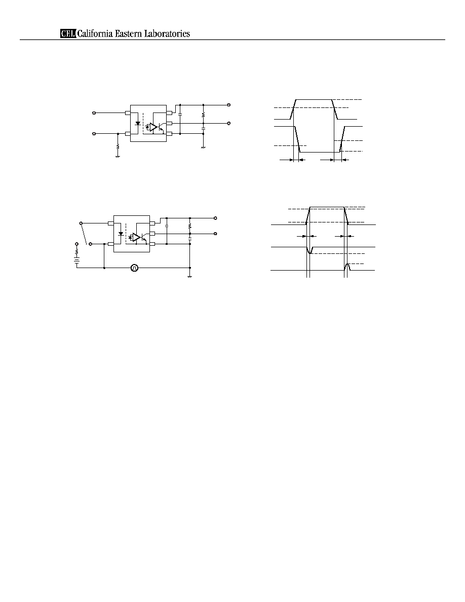
*2 Test circuit for propagation delay time
C
L
includes probe and stray wiring capacitance.
Pulse input (I
F
= 10 mA)
47
(PW = 10 s,
Duty cycle = 1/10)
�
R
L
= 20 k
V
O
(Monitor)
V
CC
= 15 V
Input
(Monitor)
0.1 F
�
C
L
= 100 pF
Input
Output
V
THHL
= 1.5 V
V
THLH
= 2.0 V
15 V
V
OL
t
PHL
t
PLH
I
F
(ON)
50% I
F
(ON)
*3 Test circuit for common mode transient immunity
C
L
includes probe and stray wiring capacitance.
90%
10%
1.5 kV
0 V
15 V
3.0 V
1.0 V
V
OL
V
CM
t
r
t
f
V
O
(Switch A: I
F
= 0 mA)
V
O
(Switch B: I
F
= 10 mA)
V
O
(Monitor)
R
L
= 20 k
C
L
= 100 pF
V
CC
= 15 V
0.1 F
�
V
CM
SW I
F
B
A
USAGE CAUTIONS
1. This product is weak for static electricity by designed with high-speed integrated circuit so protect against static
electricity when handling.
2. By-pass capacitor of 0.1
�
F is used between V
CC
and GND near device. Also, ensure that the distance between
the leads of the photocoupler and capacitor is no more than 10 mm.
3. Avoid storage at a high temperature and high humidity.
Data Sheet PN10265EJ03V0DS
6
PS9113
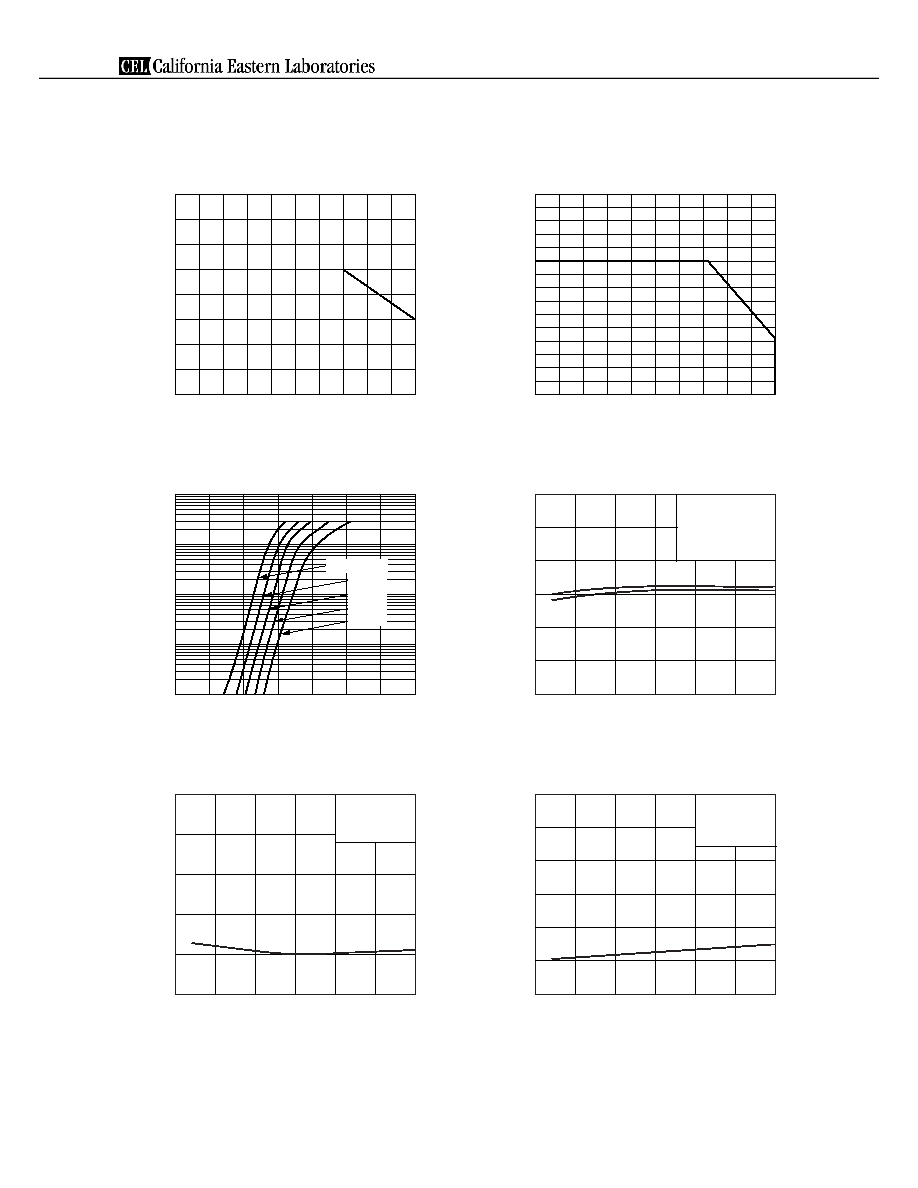
TYPICAL CHARACTERISTICS (T
A
= 25
�
C unless otherwise specified)
20
40
60
80
100
0
10
20
30
40
20
40
60
80
100
0
50
100
150
�50
�25
0
0.1
0.2
0.3
0.4
0.5
25
0
50
75
100
0
1
2
3
4
5
V
CC
= 15 V,
V
O
= 0.8 V,
I
O
= 0.75 mA
�50
�25
0
25
50
75
100
0
400
200
600
1 000
800
1 200
V
CC
= 30 V,
V
O
= Open,
I
CCH
: V
F
= 0.8 V,
I
CCL
: I
F
= 10 mA
I
CCL
I
CCH
0.6
�50
�25
0
25
50
75
100
� �
V
CC
= 15 V,
I
F
= 10 mA,
I
O
= 2.4 mA
Ambient Temperature T
A
(�C)
Maxim
um F
orw
ard Current I
F
(mA)
MAXIMUM FORWARD CURRENT
vs. AMBIENT TEMPERATURE
Ambient Temperature T
A
(�C)
Detector P
o
w
er Dissipation P
C
(mW)
DETECTOR POWER DISSIPATION
vs. AMBIENT TEMPERATURE
Ambient Temperature T
A
(�C)
High Le
v
el Supply Current I
CCH
(
A),
Lo
w Le
v
el Supply Current I
CCL
(
A)
SUPPLY CURRENT vs.
AMBIENT TEMPERATURE
Ambient Temperature T
A
(�C)
Threshold Input Current I
FHL
(mA)
THRESHOLD INPUT CURRENT vs.
AMBIENT TEMPERATURE
Ambient Temperature T
A
(�C)
Lo
w Le
v
el Output
V
oltage
V
OL
(V)
LOW LEVEL OUTPUT VOLTAGE vs.
AMBIENT TEMPERATURE
Forward Voltage V
F
(V)
F
orw
ard Current I
F
(mA)
FORWARD CURRENT vs.
FORWARD VOLTAGE
1.0
0.01
0.1
1
10
100
1.2
1.4
1.6
1.8
2.0
2.2
2.4
T
A
= +85�C
+50�C
+25�C
0�C
�25�C
Remark The graphs indicate nominal characteristics.
Data Sheet PN10265EJ03V0DS
7
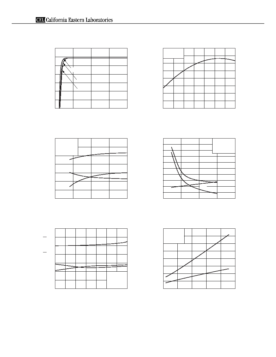
PS9113
Output Current I
O
(mA)
Forward Current I
F
(mA)
Ambient Temperature T
A
(�C)
Output Current (Relativ
e
V
alue)
0
5
10
15
20
�40
�20
0
20
40
60
80
100
Load Capacitance C
L
(pF)
Propagation Dela
y
Time t
PHL
, t
PLH
(ns)
0
100
200
300
400
500
600
700
0.70
0.80
0.75
0.85
0.95
1.05
0.90
1.00
1.10
I
F
= 10 mA,
V
CC
= 15 V,
C
L
= 100 pF,
R
L
= 20 k
I
F
= 10 mA,
V
O
= 0.6 V
I
F
= 10 mA,
C
L
= 100 pF,
R
L
= 20 k
V
CC
= 15 V,
C
L
= 100 pF,
R
L
= 20 k
I
F
= 10 mA,
V
CC
= 15 V,
R
L
= 20 k
�40
�20
0
20
40
60
80
100
0
100
200
300
400
500
600
700
0
200
400
600
800
1 000
1 200
1 400
1 600
0
100
200
300
400
500
0
10
20
30
0
200
400
600
800
1 000
1 200
1 400
1 600
1 800
�200
t
PHL
t
PLH
t
PLH
� t
PHL
PWD
t
PHL
t
PLH
t
PLH
� t
PHL
t
PHL
t
PLH
t
PLH
40
t
PHL
Forward Current I
F
(mA)
Propagation Dela
y
Time t
PHL
, t
PLH
(ns),
Maxim
um Propagation Dela
ys t
PLH
� t
PHL
(ns)
PROPAGATION DELAY TIME,
MAXIMUM PROPAGATION DELAYS
vs. FORWARD CURRENT
Ambient Temperature T
A
(�C)
PROPAGATION DELAY TIME,
PULSE WIDTH DISTORTION
vs. AMBIENT TEMPERATURE
Supply Voltage V
CC
(V)
Propagation Dela
y
Time t
PHL
, t
PLH
(ns),
Maxim
um Propagation Dela
ys t
PLH
� t
PHL
(ns)
PROPAGATION DELAY TIME,
MAXIMUM PROPAGATION DELAYS
vs. SUPPLY VOLTAGE
PROPAGATION DELAY TIME vs.
LOAD CAPACITANCE
OUTPUT CURRENT vs. FORWARD CURRENT
OUTPUT CURRENT vs.
AMBIENT TEMPERATURE
0
5
10
15
20
0
2
4
6
8
10
12
14
V
O
= 0.6 V
�40�C
+100�C
T
A
= +25�C
Propagation Dela
y
Time t
PHL
, t
PLH
(ns),
Pulse
Width Distor
tion t
PHL
� t
PLH
(ns)
Remark The graphs indicate nominal characteristics.
Data Sheet PN10265EJ03V0DS
8
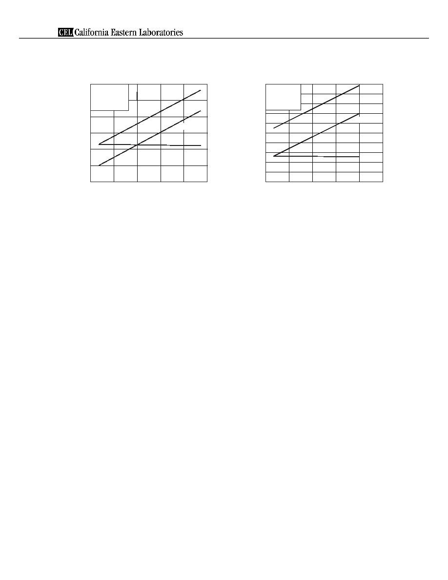
PS9113
I
F
= 10 mA,
V
CC
= 15 V,
C
L
= 100 pF
I
F
= 10 mA,
V
CC
= 5 V,
C
L
= 15 pF
0
5
10
15
20
25
50
100
150
200
250
300
350
400
450
500
0
0
10
20
30
40
50
�200
200
0
400
800
600
1 000
t
PHL
t
PLH
t
PHL
t
PLH
t
PLH
� t
PHL
t
PLH
� t
PHL
Load Resistance R
L
(k
)
Propagation Dela
y
Time t
PHL
, t
PLH
(ns),
Maxim
um Propagation Dela
ys t
PLH
� t
PHL
(ns)
PROPAGATION DELAY TIME,
MAXIMUM PROPAGATION DELAYS
vs. LOAD RESISTANCE
Load Resistance R
L
(k
)
Propagation Dela
y
Time t
PHL
, t
PLH
(ns),
Maxim
um Propagation Dela
ys t
PLH
� t
PHL
(ns)
PROPAGATION DELAY TIME,
MAXIMUM PROPAGATION DELAYS
vs. LOAD RESISTANCE
Remark The graphs indicate nominal characteristics.
Data Sheet PN10265EJ03V0DS
9
PS9113
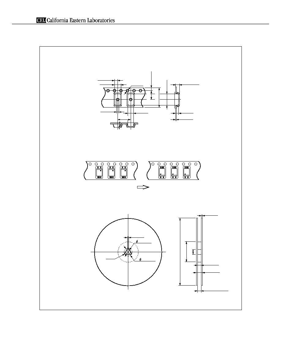
TAPING SPECIFICATIONS (UNIT: mm)
Outline and Dimensions (Tape)
Tape Direction
Outline and Dimensions (Reel)
Packing: 2 500 pcs/reel
100�1.0
13.0�0.2
330�2.0
2.0�0.5
11.9 to 15.4
Outer edge of
flange
17.5�1.0
13.5�1.0
2.0�0.5
13.0�0.2
R 1.0
21.0�0.8
PS9113-F3
PS9113-F4
1.55�0.1
2.0�0.05
4.0�0.1
1.75�0.1
3.9�0.1
3.45 MAX.
7.4�0.1
0.3
�0.05
8.0�0.1
1.5
+0.1
�0
5.5�0.1
12.0�0.2
3.0�0.1
Data Sheet PN10265EJ03V0DS
10
PS9113
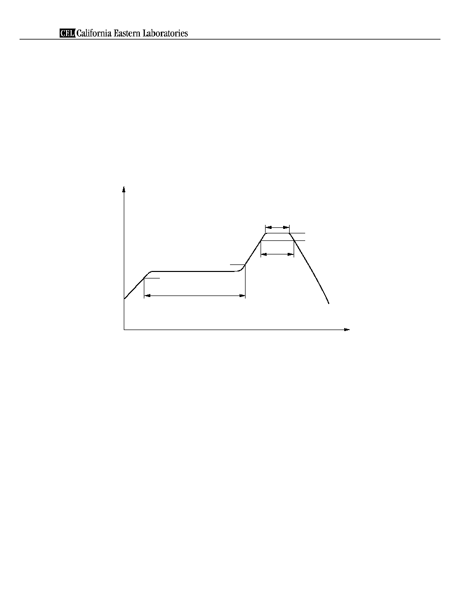
NOTES ON HANDLING
1. Recommended soldering conditions
(1) Infrared reflow soldering
� Peak reflow temperature
260
�
C or below (package surface temperature)
� Time of peak reflow temperature
10 seconds or less
� Time of temperature higher than 220
�
C
60 seconds or less
� Time to preheat temperature from 120 to 180
�
C 120
�
30 s
� Number of reflows
Three
� Flux
Rosin flux containing small amount of chlorine (The flux with a
maximum chlorine content of 0.2 Wt% is recommended.)
120�30 s
(preheating)
220�C
180�C
Package Surface Temperature T (�C)
Time (s)
Recommended Temperature Profile of Infrared Reflow
(heating)
to 10 s
to 60 s
260�C MAX.
120�C
(2) Wave soldering
� Temperature
260
�
C or below (molten solder temperature)
� Time
10 seconds or less
� Preheating conditions
120
�
C or below (package surface temperature)
� Number of times
One (Allowed to be dipped in solder including plastic mold portion.)
� Flux
Rosin flux containing small amount of chlorine (The flux with a maximum chlorine
content of 0.2 Wt% is recommended.)
(3) Soldering by Soldering Iron
� Peak Temperature (lead part temperature) 350
�
C or below
� Time (each pins)
3 seconds or less
� Flux
Rosin flux containing small amount of chlorine (The flux with a
maximum chlorine content of 0.2 Wt% is recommended.)
(a) Soldering of leads should be made at the point 1.5 to 2.0 mm from the root of the lead
(b) Please be sure that the temperature of the package would not be heated over 100
�
C
Data Sheet PN10265EJ03V0DS
11

PS9113
(4) Cautions
� Fluxes
Avoid removing the residual flux with freon-based and chlorine-based cleaning solvent.
2. Cautions regarding noise
Be aware that when voltage is applied suddenly between the photocoupler's input and output or between
collector-emitters at startup, the output transistor may enter the on state, even if the voltage is within the absolute
maximum ratings.
USAGE CAUTIONS
1. Protect against static electricity when handling.
2. Avoid storage at a high temperature and high humidity.
Data Sheet PN10265EJ03V0DS
12
4590 Patrick Henry Drive
Santa Clara, CA 95054-1817
Telephone: (408) 919-2500
Facsimile: (408) 988-0279
Subject: Compliance with EU Directives
CEL certifies, to its knowledge, that semiconductor and laser products detailed below are compliant
with the requirements of European Union (EU) Directive 2002/95/EC Restriction on Use of Hazardous
Substances in electrical and electronic equipment (RoHS) and the requirements of EU Directive
2003/11/EC Restriction on Penta and Octa BDE.
CEL Pb-free products have the same base part number with a suffix added. The suffix �A indicates
that the device is Pb-free. The �AZ suffix is used to designate devices containing Pb which are
exempted from the requirement of RoHS directive (*). In all cases the devices have Pb-free terminals.
All devices with these suffixes meet the requirements of the RoHS directive.
This status is based on CEL's understanding of the EU Directives and knowledge of the materials that
go into its products as of the date of disclosure of this information.
Restricted Substance
per RoHS
Concentration Limit per RoHS
(values are not yet fixed)
Concentration contained
in CEL devices
-A -AZ
Lead (Pb)
< 1000 PPM
Not Detected
(*)
Mercury
< 1000 PPM
Not Detected
Cadmium
< 100 PPM
Not Detected
Hexavalent Chromium
< 1000 PPM
Not Detected
PBB
< 1000 PPM
Not Detected
PBDE
< 1000 PPM
Not Detected
If you should have any additional questions regarding our devices and compliance to environmental
standards, please do not hesitate to contact your local representative.
Important Information and Disclaimer: Information provided by CEL on its website or in other communications concerting the substance
content of its products represents knowledge and belief as of the date that it is provided. CEL bases its knowledge and belief on information
provided by third parties and makes no representation or warranty as to the accuracy of such information. Efforts are underway to better
integrate information from third parties. CEL has taken and continues to take reasonable steps to provide representative and accurate
information but may not have conducted destructive testing or chemical analysis on incoming materials and chemicals. CEL and CEL
suppliers consider certain information to be proprietary, and thus CAS numbers and other limited information may not be available for
release.
In no event shall CEL's liability arising out of such information exceed the total purchase price of the CEL part(s) at issue sold by CEL to
customer on an annual basis.
See CEL Terms and Conditions for additional clarification of warranties and liability.