1
CAT24C44
256-Bit Serial Nonvolatile CMOS Static RAM
FEATURES
s
Single 5V Supply
s
Infinite E
2
PROM to RAM Recall
s
CMOS and TTL Compatible I/O
s
Low CMOS Power Consumption:
Active: 3 mA Max.
Standby: 30
µ
A Max.
s
Power Up/Down Protection
s
10 Year Data Retention
s
JEDEC Standard Pinouts:
8-pin DIP
8-pin SOIC
s
100,000 Program/Erase Cycles (E
2
PROM)
s
Auto Recall on Power-up
s
Commercial, Industrial and Automotive
Temperature Ranges
DESCRIPTION
The CAT24C44 Serial NVRAM is a 256-bit nonvolatile
memory organized as 16 words x 16 bits. The high
speed Static RAM array is bit for bit backed up by a
nonvolatile E
2
PROM array which allows for easy trans-
fer of data from RAM array to E
2
PROM (STORE) and
from E
2
PROM to RAM (RECALL). STORE operations
are completed in 10ms max. and RECALL operations
typically within 1.5
µ
s. The CAT24C44 features unlimited
RAM write operations either through external RAM
writes or internal recalls from E
2
PROM. Internal false
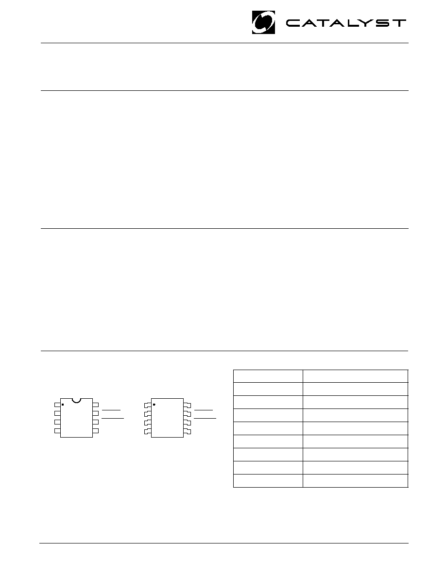
PIN CONFIGURATION
store protection circuitry prohibits STORE operations
when V
CC
is less than 3.5V (typical) ensuring E
2
PROM
data integrity.
The CAT24C44 is manufactured using Catalyst's ad-
vanced CMOS floating gate technology. It is designed to
endure 100,000 program/erase cycles (E
2
PROM) and
has a data retention of 10 years. The device is available
in JEDEC approved 8-pin plastic DIP and SOIC pack-
ages.
PIN FUNCTIONS
Pin Name
Function
SK
Serial Clock
DI
Serial Input
DO
Serial Data Output
CE
Chip Enable
RECALL
Recall
STORE
Store
V
CC
+5V
V
SS
Ground
SOIC Package (S)
DI
DO
1
2
3
4
CE
SK
RECALL
VSS
VCC
STORE
8
7
6
5
1
2
3
4
8
7
6
5
CE
SK
DI
DO
VCC
RECALL
VSS
STORE
DIP Package (P)
5157 FHD F01
© 1998 by Catalyst Semiconductor, Inc.
Characteristics subject to change without notice
Doc. No. 25019-0A 2/98 N-1

2
CAT24C44
Doc. No. 25019-0A 2/98 N-1
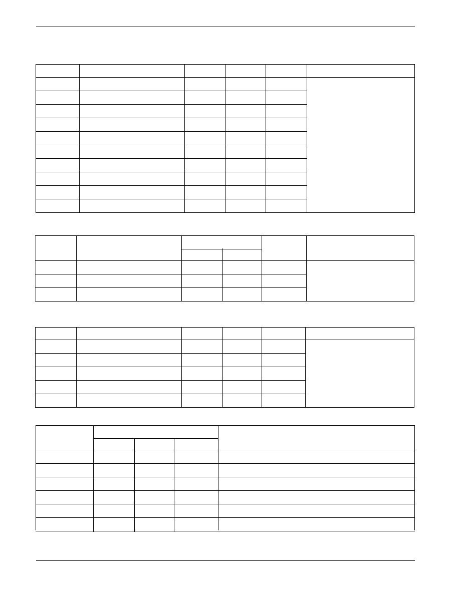
POWER-UP TIMING
(4)
Symbol
Parameter
Min.
Max.
Units
VCCSR
V
CC
Slew Rate
0.5
0.005
V/m
t
pur
Power-Up to Read Operations
200
µ
s
t
puw
Power-Up to Write or Store Operation
5
ms
MODE SELECTION
(1)(2)
Software
Write Enable
Previous Recall
Mode
STORE
STORE
STORE
STORE
STORE
RECALL
RECALL
RECALL
RECALL
RECALL
Instruction
Latch
Latch
Hardware Recall
(3)
1
0
NOP
X
X
Software Recall
1
1
RCL
X
X
Hardware Store
(3)
0
1
NOP
SET
TRUE
Software Store
1
1
STO
SET
TRUE
X = Don't Care
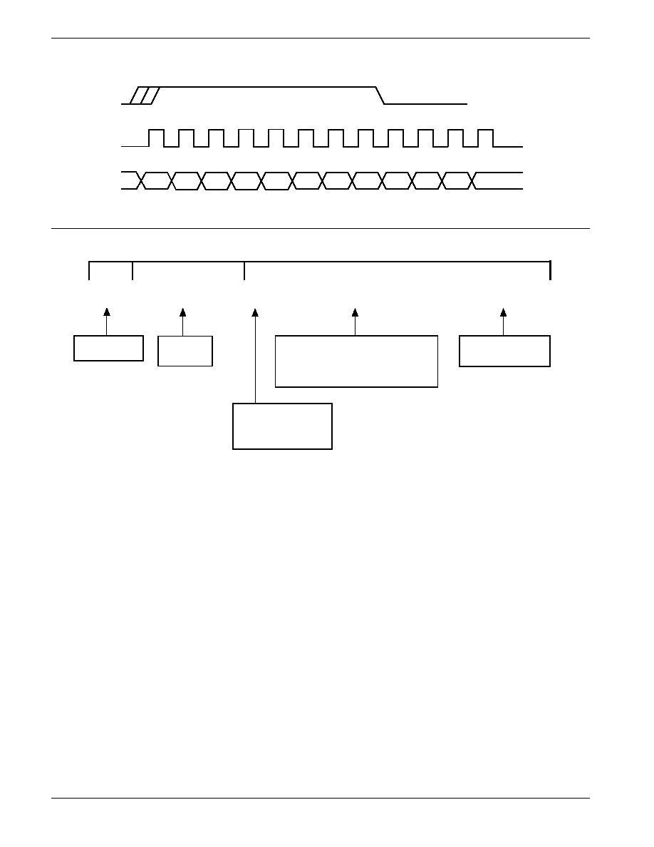
BLOCK DIAGRAM
5157 FHD F09
ROW
DECODE
INSTRUCTION
REGISTER
COLUMN
DECODE
E
2
PROM ARRAY
STORE
RECALL
STATIC RAM
ARRAY
256-BIT
STORE
RECALL
CE
DI
SK
INSTRUCTION
DECODE
4-BIT
COUNTER
CONTROL
LOGIC
VCC
VSS
DO
Note:
(1) The store operation has priority over all the other operations.
(2) The store operation is inhibited when V
CC
is below
3.5V.
(3) NOP designates that the device is not currently executing an instruction.
(4) This parameter is tested initially and after a design or process change that affects the parameter.

CAT24C44
3
Doc. No. 25019-0A 2/98 N-1
ABSOLUTE MAXIMUM RATINGS*
Temperature Under Bias ................. 55
°
C to +125
°
C
Storage Temperature ....................... 65
°
C to +150
°
C
Voltage on Any Pin with
Respect to Ground
(2)
............. 2.0 to +VCC +2.0V
V
CC
with Respect to Ground ............... 2.0V to +7.0V
Package Power Dissipation
Capability (Ta = 25
°
C) ................................... 1.0W
Lead Soldering Temperature (10 secs) ............ 300
°
C
Output Short Circuit Current
(3)
........................ 100 mA
*COMMENT
Stresses above those listed under "Absolute Maximum
Ratings" may cause permanent damage to the device.
These are stress ratings only, and functional operation
of the device at these or any other conditions outside of
those listed in the operational sections of this specifica-
tion is not implied. Exposure to any absolute maximum
rating for extended periods may affect device perfor-
mance and reliability.
Note:
(1) This parameter is tested initially and after a design or process change that affects the parameter.
(2) The minimum DC input voltage is 0.5V. During transitions, inputs may undershoot to 2.0V for periods of less than 20 ns.
Maximum DC voltage on output pins is V
CC
+0.5V, which may overshoot to V
CC
+2.0V for periods of less than 20 ns.
(3) Output shorted for no more than one second. No more than one output shorted at a time.
(4) Latch-up protection is provided for stresses up to 100 mA on address and data pins from 1V to V
CC
+1V.
RELIABILITY CHARACTERISTICS
Symbol
Parameter
Min.
Max.
Units
Reference Test Method
N
END
(1)
Endurance
100,000
Cycles/Byte
MIL-STD-883, Test Method 1033
T
DR
(1)
Data Retention
10
Years
MIL-STD-883, Test Method 1008
V
ZAP
(1)
ESD Susceptibility
2000
Volts
MIL-STD-883, Test Method 3015
I
LTH
(1)(4)
Latch-Up
100
mA
JEDEC Standard 17
CAPACITANCE T
A
= 25
°
C, f = 1.0 MHz, V
CC
= 5V
Symbol
Parameter
Max.
Unit
Conditions
C
I/O
(1)
Input/Output Capacitance
10
pF
V
I/O
= 0V
C
IN
(1)
Input Capacitance
6
pF
V
IN
= 0V
D.C. OPERATING CHARACTERISTICS
V
CC
= 5V
±
10%, unless otherwise specified.
Limits
Symbol
Parameter
Min.
Typ.
Max.
Unit
Conditions
I
CCO
Current Consumption (Operating)
3
mA
Inputs = 5.5V, T
A
= 0
°
C
All Outputs Unloaded
I
SB
Current Consumption (Standby)
30
µ
A
CE = V
IL
I
LI
Input Current
2
µ
A
0
V
IN
5.5V
I
LO
Output Leakage Current
10
µ
A
0
V
OUT
5.5V
V
IH
High Level Input Voltage
2
V
CC
V
V
IL
Low Level Input Voltage
0
0.8
V
V
OH
High Level Output Voltage
2.4
V
I
OH
= 2mA
V
OL
Low Level Output Voltage
0.4
V
I
OL
= 4.2mA
4
CAT24C44
Doc. No. 25019-0A 2/98 N-1
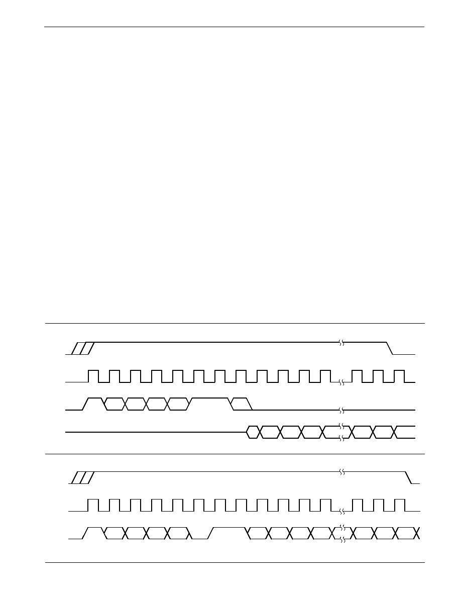
A.C. CHARACTERISTICS
V
CC
= 5V
±
10%, unless otherwise specified.
Symbol
Parameter
Min.
Max.
Units
Conditions
F
SK
SK Frequency
DC
1
MHz
t
SKH
SK Positive Pulse Width
400
ns
t
SKL
SK Negative Pulse Width
400
ns
C
L
= 100pF + 1TTL gate
t
DS
Data Setup Time
400
ns
V
OH
= 2.2V, V
OL
= 0.65V
t
DH
Data Hold Time
80
ns
V
IH
= 2.2V, V
IL
= 0.65V
t
PD
SK Data Valid Time
375
ns
Input rise and fall times = 10ns
t
Z
CE Disable Time
1
µ
s
t
CES
CE Enable Setup Time
800
ns
t
CEH
CE Enable Hold Time
400
ns
t
CDS
CE De-Select Time
800
ns
A.C. CHARACTERISTICS, Store Cycle
V
CC
= 5V
±
10%, unless otherwise specified.
Limits
Symbol
Parameter
Min.
Max.
Units
Conditions
t
ST
Store Time
10
ms
C
L
= 100pF + 1TTL gate
t
STP
Store Pulse Width
200
ns
V
OH
= 2.2V, V
OL
= 0.65V
t
STZ
Store Disable Time
100
ns
V
IH
= 2.2V, V
IL
= 0.65V
A.C. CHARACTERISTICS, Recall Cycle
V
CC
= 5V
±
10%, unless otherwise specified.
Symbol
Parameter
Min.
Max.
Units
Conditions
t
RCC
Recall Cycle Time
2.5
µ
s
t
RCP
Recall Pulse Width
500
ns
C
L
= 100pF + 1TTL gate
t
RCZ
Recall Disable Time
500
ns
V
OH
= 2.2V, V
OL
= 0.65V
t
ORC
Recall Enable Time
10
ns
V
IH
= 2.2V, V
IL
= 0.65V
t
ARC
Recall Data Access Time
1.5
µ
s
INSTRUCTION SET
Format
Instruction
Start Bit
Address
OP Code
Operation
WRDS
1
XXXX
0 0 0
Reset Write Enable Latch (Disables, Writes and Stores)
STO
1
XXXX
0 0 1
Store RAM Data in E
2
PROM
WRITE
1
AAAA
0 1 1
Write Data into RAM Address AAAA
WREN
1
XXXX
1 0 0
Set Write Enable Latch (Enables, Writes and Stores)
RCL
1
XXXX
1 0 1
Recall E
2
PROM Data into RAM
READ
1
AAAA
1 1 X
Read Data From RAM Address AAAA
X = Don't care
A = Address bit
CAT24C44
5
Doc. No. 25019-0A 2/98 N-1
DEVICE OPERATION
The CAT24C44 is intended for use with standard micro-
processors. The CAT24C44 is organized as 16 registers
by 16 bits. Seven 8-bit instructions control the device's
operating modes, the RAM reading and writing, and the
E
2
PROM storing and recalling. It is also possible to
control the E
2
PROM store and recall functions in hard-
ware with the
STORE
and
RECALL
pins. The CAT24C44
operates on a single 5V supply and will generate, on
chip, the high voltage required during a RAM to E
2
PROM
storing operation.
Instructions, addresses and write data are clocked into
the DI pin on the rising edge of the clock (SK). The DO
pin remains in a high impedance state except when
outputting data from the device. The
CE
(Chip Enable)
pin must remain high during the entire data transfer.
The format for all instructions sent to the CAT24C44 is
a logical `1' start bit, 4 address bits (data read or write
operations) or 4 "Don't Care" bits (device mode opera-
tions), and a 3-bit op code (see Instruction Set). For data
write operations, the 8-bit instruction is followed by 16
bits of data. For data read instructions, DO will come out
of the high impedance state and enable 16 bits of data
to be clocked from the device. The 8th bit of the read
instruction is a "Don't Care" bit. This is to eliminate any
bus contention that would occur in applications where
the DI and DO pins are tied together to form a common
DI/DO line. A word of caution while clocking data to and
from the device: If the
CE
pin is prematurely deselected
while shifting in an instruction, that instruction will not be
executed, and the shift register internal to the CAT24C44
will be cleared. If there are more than or less than 16
clocks during a memory data transfer, an improper data
transfer will result. The SK clock is completely static
allowing the user to stop the clock and restart it to
resume shifting of data.
Read
Upon receiving a start bit, 4 address bits, and the 3-bit
read command (clocked into the DI pin), the DO pin of
the CAT24C44 will come out of the high impedance state
and the 16 bits of data, located at the address specified
in the instructions, will be clocked out of the device.
When clocking data from the device, the first bit clocked
out (DO) is timed from the falling edge of the 8th clock,
all succeeding bits (D1D15) are timed from the rising
edge of the clock.
Write
After receiving a start bit, 4 address bits, and the 3-bit
WRITE command, the 16-bit word is clocked into the
device for storage into the RAM memory location speci-
fied. The
CE
pin must remain high during the entire write
operation.
Figure 1. RAM Read Cycle Timing
5157 FHD F02
Note:
(1) Bit 8 of READ instruction is "Don't Care".
Figure 2. RAM Write Cycle Timing
5157 FHD F03
SK
CE
DI
D0
1
2
3
4
5
6
7
8
9
10
11
12
22
23
24
1
D1
D2
D3
D13
D14
D15
A
1
1
A
A
A
0
SK
CE
DI
DO
HIGH-Z
D0
1
2
3
4
5
6
7
8
9
10
11
12
22
23
24
1
D1
D2
D3
D14
D15
D0
A
X
1
1
A
A
A
(8)
(1)

6
CAT24C44
Doc. No. 25019-0A 2/98 N-1
WREN/WRDS
The CAT24C44 powers up in the program disable state
(the "write enable latch" is reset). Any programming
after power-up or after a WRDS (RAM write/E
2
PROM
store disable) instruction must first be preceded by the
WREN (RAM write/E
2
PROM store enable) instruction.
Once writing/storing is enabled, it will remain enabled
until power to the device is removed, the WRDS instruc-
tion is sent, or an E
2
PROM store has been executed
5157 FHD F05
Figure 4. Write Cycle Timing
Figure 3. Read Cycle Timing
5157 FHD F04
x
1
2
n
SK
CE
tSKL
tSKH
1/FSK
tCEH
tDH
tDS
tCES
tCDS
DI
HIGH-Z
tPD
6
7
8
9
10
11
tPD
tZ
VIH
HIGH-Z
SK CYCLE #
SK
CE
DI
DO
D0
D1
Dn
(STO). The WRDS (write/store disable) can be used to
disable all CAT24C44 programming functions, and will
prevent any accidental writing to the RAM, or storing to
the E
2
PROM.
Data can be read normally from the CAT24C44 regard-
less of the "write enable latch" status.

CAT24C44
7
Doc. No. 25019-0A 2/98 N-1
RCL/
RECALL
RECALL
RECALL
RECALL
RECALL
Data is transferred from the E
2
PROM data memory to
RAM by either sending the RCL instruction or by pulling
the
RECALL
input pin low. A recall operation must be
performed before the E
2
PROM store, or RAM write
operations can be executed. Either a hardware or soft-
ware recall operation will set the "previous recall" latch
internal to the CAT24C44.
POWER-ON RECALL
The CAT24C44 has a power-on recall function that
transfers the E
2
PROM data to the RAM. After Power-up,
all functions are inhibited for at least 200ns (T
pur
) from
stable V
cc
.
STO/
STORE
STORE
STORE
STORE
STORE
Data in the RAM memory area is stored in the E
2
PROM
memory either by sending the STO instruction or by
pulling the
STORE
input pin low. As security against any
inadvertent store operations, the following conditions
must each be met before data can be transferred into
nonvolatile storage:
· The "previous recall" latch must be set (either a
software or hardware recall operation).
· The "write enable" latch must be set (WREN
instruction issued).
· STO instruction issued or
STORE
input low.
During the store operation, all other CAT24C44 func-
tions are inhibited. Upon completion of the store opera-
tion, the "write enable" latch is reset. The device also
provides false store protection whenever V
CC
falls below
a 3.5V level. If V
CC
falls below this level, the store
operation is disabled and the "write enable" latch is
reset.
Figure 6. Hardware Store Cycle Timing
5157 FHD F07
Figure 5. Recall Cycle Timing
5157 FHD F06
RECALL
tRCZ
tORC
tRCC
tRCP
tARC
VALID DATA
UNDEFINED DATA
DO
HIGH-Z
STORE
tST
tSTP
DO
tSTZ
HIGH-Z
8
CAT24C44
Doc. No. 25019-0A 2/98 N-1
Figure 7. Non-Data Operations
SK
CE
DI
1
2
3
4
5
6
7
8
1
X
X
X
X
OP-CODE
5157 FHD F08
24C44 F11
ORDERING INFORMATION
Notes:
(1) The device used in the above example is a 24C44SI-TE13 (SOIC, Industrial Temperature, Tape & Reel)
Prefix
Device #
Suffix
24C44
S
I
-TE13
Product
Number
Tape & Reel
TE13: 2000/Reel
Package
P: PDIP
S: SOIC (JEDEC)
CAT
Temperature Range
Blank = Commercial (0° - 70°C)
I = Industrial (-40° - 85°C)
A = Automotive (-40° - 105°C)*
* -40° to +125°C is available upon request
Optional
Company ID