® 2003 California Micro Devices Corp. All rights reserved.
10/01/03
430 N. McCarthy Blvd., Milpitas, CA 95035-5112
L Tel: 408.263.3214
L Fax: 408.263.7846 L www.calmicro.com
1
CM2400-01
Universal Serial Bus Transceiver with Level Translator
Features
Ę
Complies with USB Specification Rev 1.1 & 2.0
Ę
Supports Full Speed Mode (12Mbit/sec.)
Ę
Integrated 5V to 3.3V regulator
Ę
Used as a USB device transceiver
Ę
V
BUS
disconnection indication through V
P
, V
M
Ę
Two single-ended receivers with hysteresis
Ę
USB Detection of V
BUS
via level translator
Ę
Stable RCV output during SE0 condition
Ę
Low power operation
Ę
Supports 1.65V to 3.3V I/O voltage levels
Ę
Full industrial operating range -40 to 85 ░C
Ę
Available in small HBCC16 package
Applications
Ę
Wireless handsets
Ę
Digital still cameras
Ę
PDAs (Personal Digital Assistants)
Ę
IAs (Information Appliances)
Product Description
The CM2400-01HB Universal Serial Bus (USB) trans-
ceiver is fully compliant with the USB specification Rev
1.1 and 2.0. It supports a speed of 12Mbits/s (Full
Speed Mode).
An internal level shifter allows interface to Application
Specific IC's (ASIC's) and Programmable Logic
Devices (PLD's) running at core voltages of 1.65V to
3.3V.
An internal 5V to 3.3V regulator is used to power the
CM2400-01HB USB transceiver via the USB supply
V
BUS
. A voltage comparator has been integrated to
detect the V
BUS
voltage via the level translator. This
insures compatibility with the processor's core voltage
and outputs to the USB_DET pin. A high level on the
USB_DET output indicates that an active USB cable is
attached. Single and differential input modes are
selectable by a mode input pin (MODE).
This device is ideal for portable electronic devices such
as mobile phones, digital still cameras, PDAs (Personal
Digital Assistants) and IAs (Information Appliances).
The CM2400-01HB is packaged in a small form-factor
16-lead HBCC package to conserve board space.
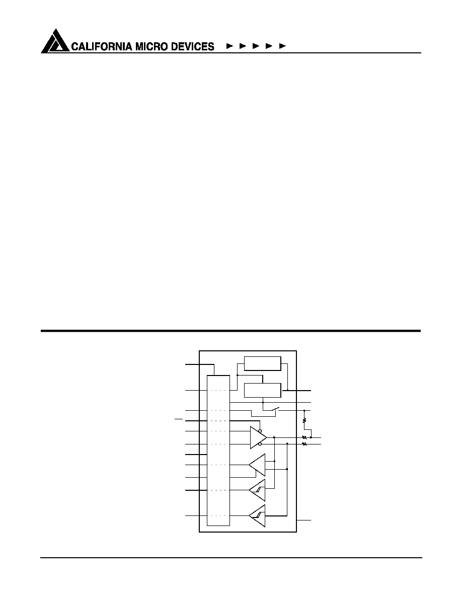
Simplified Block Schematic
Voltage
Detector
Voltage
Regulator
VCC
USB_DET
ENUM
OE
V
MO
/FSEO
V
PO
/V
O
RCV
SPND
V
P
V
M
GND
D-
D+
V
PU
V
REG
V
BUS
ENABLE
MODE
LE
V
E
L TR
A
N
S
L
A
T
OR

® 2003 California Micro Devices Corp. All rights reserved.
2
430 N. McCarthy Blvd., Milpitas, CA 95035-5112
L Tel: 408.263.3214
L Fax: 408.263.7846 L www.calmicro.com
10/01/03
CM2400-01
PIN DESCRIPTIONS
PINS
NAME
DESCRIPTION
1
OE
Input for Output Enable (Active low). Enables transceiver driver to transmit data on the USB bus.
When OE pin = LOW, driver circuitry is enabled.
2
RCV
Differential receiver output of D+ and D- input data lines. The output state of RCV is preserved and
stable during an SE0 condition.
3
V
P
Single-ended D+ receiver output for detection of a single-ended zero or error conditions
4
V
M
Single-ended D- receiver output for detection of a single-ended zero or error conditions.
5
SPND
Suspend input. Allows the device to enter a low power state while the USB is inactive.
6
MODE
Mode input. Selects between differential (V
PO
, V
MO
) and single-ended mode (V
O
, FSEO).
7
V
CC
Supply voltage for digital I/O pins. Voltages supported: 1.65 to 3.3V.
8
USB_DET
I/O level USB detect output. Logic High indicates that a USB cable is present.
9
D-
Negative USB data connection.
10
D+
Positive USB data connection. In full-speed connect mode, connect to V
PU
via a 1.5k
resistor. Tol-
erance of this resistor is defined in the USB specification REV 1.1 & 2.0
11
V
PO
/V
O
Driver data input.
12
V
MO
/FSEO
Driver data input.
13
V
REG
Regulated supply voltage output during USB operation of V
BUS
. 1uF decoupling capacitor is
required.
14
V
BUS
Supply voltage input. Can be directly connected to USB V
BUS
.
15
V
PU
Pull-up supply voltage. Pin function is controlled by input ENUM.
PACKAGE / PINOUT DIAGRAM
Note: This drawing is not to scale.
Bottom View
HBCC16 Package
5
4
3
2
1
16
15 14
6
7
8
10
11
12
9
13
GND
HBCC16
17
SPND
V
M
V
P
RCV
OE
ENUM
V
BU
S
V
PU
V
REG
V
MO
/FSEO
V
PO
/V
O
D+
D-
USB DET
V
CC
MOD
E

® 2003 California Micro Devices Corp. All rights reserved.
10/01/03
430 N. McCarthy Blvd., Milpitas, CA 95035-5112
L Tel: 408.263.3214
L Fax: 408.263.7846
L www.calmicro.com
3
CM2400-01
Ordering Information
Note 1: Parts are shipped in Tape & Reel form unless otherwise specified.
Specifications
Note 1: Equivalent to discharging a 100pF capacitor via a 1.5k
resistor (Human body model).
16
ENUM
Enumerate, allows software to control connection of the external pull-up via the level translator. If
ENUM = LOW then V
PU
is floating. If ENUM = HIGH then V
PU
is internally connected to V
REG
.
17
GND
The ground terminal is connected to the exposed diepad (heatsink).
PIN DESCRIPTIONS
PART NUMBERING INFORMATION
PADS
Package
Ordering Part Number
1
Part Marking
16
HBCC16
CM2400-01HB
CMD240001A
ABSOLUTE MAXIMUM RATINGS
PARAMETER
RATING
UNITS
ESD Protection (HBM, All Pins, See Note 1)
+2000
V
V
BUS
[GND - 0.5] to +5.5
V
V
CC
[GND - 0.5] to +6.0
V
V
I
(INPUT)
[GND - 0.5] to [V
CC
+ 0.5]
V
Storage Temperature Range
-65 to +150
░C
Operating Temperature Range
Junction
-40 to +150
░C
STANDARD (RECOMMENDED) OPERATING CONDITIONS
SYMBOL
PARAMETER
MIN
TYP
MAX
UNITS
V
BUS
USB V
BUS
Supply
4.1
5.0
5.5
V
V
CC
DC System Supply
1.65
3.3
3.6
V
V
I
DC Input Voltage
0
-
V
CC
V
V
I(AI/O)
Analog I/O Pins (D+, D-)
0
-
3.6
V
T
AMB
Ambient Operating Temperature Range
-40
-
85
░C

® 2003 California Micro Devices Corp. All rights reserved.
4
430 N. McCarthy Blvd., Milpitas, CA 95035-5112
L Tel: 408.263.3214
L Fax: 408.263.7846 L www.calmicro.com
10/01/03
CM2400-01
Specifications (cont'd)
Note 1: Operating Characteristics are over Standard Operating Conditions unless otherwise specified.
Note 2: Excluding any load current and V
PU
/VSW source current to 1.5k
and 15k pull-up and pull-down resistors (200
Ą
A).
ELECTRICAL OPERATING CHARACTERISTICS
1
Supply Pins (V
BUS
= 4.1V to 5.5V; V
CC
= 1.65V to 3.6V)
SYMBOL
PARAMETER
CONDITIONS
MIN
TYP
MAX
UNITS
V
REG
Regulated supply output
Unloaded
3.0
3.3
3.6
V
I
BUS
Operating supply current
Full-speed TX and RX; C
L
=50pF on
D+/D- outputs
10
mA
I
BUS(IDLE)
Supply current during full
speed idle and SE0
Full-speed idle; Note 2
500
ĄA
I
BUS(SUSP)
Supply current during sus-
pend
SPND = HI; Note 2
100
ĄA
I
CC
Operating I/O supply current
Full-speed TX and RX
2.0
mA
I
CC(STAT)
Static I/O supply current
Full-speed idle, SE0 or suspend
10.0
ĄA
I
CC(SHARE)
Supply current during shar-
ing mode
V
BUS
not connected
10.0
ĄA
I
DX(SHARE)
D+/D- load current during
sharing mode
V
BUS
not connected; ENUMERATE = LOW
10.0
ĄA
V
TH(VBUS)
V
BUS
supply detection
threshold, USB_D output
Supply lost (USB_D low)
3.6
V
Supply present
4.1
V
V
TH(BUS)
Hysteresis
100
mV
V
TH(VCC)
V
CC
supply detection thresh-
old.
Supply lost (USB_D low)
0.5
V
Supply present
1.4
V
V
TH(VCC)
Hysteresis
200
mV
Digital Pins (V
BUS
= 4.1V to 5.5V; V
CC
= 1.8V ▒ 0.15V)
SYMBOL
PARAMETER
CONDITIONS
MIN
TYP
MAX
UNITS
V
IL
Logic LOW input voltage
0.5
V
V
IH
Logic HIGH input voltage
1.2
V
V
OL
Logic LOW output voltage
I
OL
= 100
ĄA
I
OL
= 2mA
0.15
0.40
V
V
V
OH
Logic HIGH output voltage
I
OH
= 100
ĄA
I
OH
= 2mA
1.50
1.25
V
V
Digital Pins (V
BUS
= 4.1V to 5.5V; V
CC
= 2.5V ▒ 0.2V)
SYMBOL
PARAMETER
CONDITIONS
MIN
TYP
MAX
UNITS
V
IL
Logic LOW input voltage
0.7
V
V
IH
Logic HIGH input voltage
1.7
V
V
OL
Logic LOW output voltage
I
OL
= 100
ĄA
I
OL
= 2mA
0.15
0.40
V
V
V
OH
Logic HIGH output voltage
I
OH
= 100
ĄA
I
OH
= 2mA
2.15
1.90
V
V

® 2003 California Micro Devices Corp. All rights reserved.
10/01/03
430 N. McCarthy Blvd., Milpitas, CA 95035-5112
L Tel: 408.263.3214
L Fax: 408.263.7846
L www.calmicro.com
5
CM2400-01
Specifications (cont'd)
Note 3: Rev 2.0 states Z
DRV
must be between 28
and 44, when the driver is not high speed capable.
ELECTRICAL OPERATING CHARACTERISTICS (CONT'D)
Analog I/O Pins (V
BUS
= 4.1V to 5.5V; V
CC
= 1.65V to 3.6V)
SYMBOL
PARAMETER
CONDITIONS
MIN
TYP
MAX
UNITS
V
DI
Differential receiver input
sensitivity
|
V
I
(D+) - V
I
(D-)
|
0.2
V
V
CM
Differential receiver
common mode voltage
0.8
2.5
V
V
IL
Single-ended receiver
logic LOW input voltage
0.8
V
V
IH
Single-ended receiver
logic HIGH input voltage
2.0
V
V
HYS
Single-ended receiver
Hysteresis voltage
0.4
0.7
V
V
OL
Logic LOW output voltage
R
L
= 1.5K
tied to +3.6V
0.3
V
V
OH
Logic HIGH output voltage
R
L
= 15K
tied to GND
2.8
3.6
V
I
LZ
OFF-state leakage current
+1
ĄA
C
IN
Transceiver Capacitance
Pin to GND
10
pF
R
SW
Internal switch resistance at
V
PU
30
Z
DRV
Driver output impedance
(includes 33 ohm 1% resis-
tor)
Measured with steady-state drive; See Note 3
33
39
44
Driver Characteristics & Timings (Full-speed mode only)
SYMBOL
PARAMETER
CONDITIONS
MIN
TYP
MAX
UNITS
t
FR
Rise time
C
L
= 50 to 125pF, measured 10% to 90%
(V
OH
-V
OL
); See Figure 6
4
20
ns
t
FF
Fall time
C
L
= 50 to 125pF, measured 10% to 90%
(V
OH
-V
OL
); See Figure 6
4
20
ns
FRFM
Differential rise / fall time
matching (t
FR
/t
FF
)
Excluding the first transition from idle state
90
110
%
V
CRS
Output signal crossover
voltage
Excluding the first transition from idle state;
See Figure 9
1.3
2.0
V
t
PLH(DRV)
Driver propagation delay (V
O
/
V
PO
D+/D-, FSEO/V
MO
D+/D-
LOW-to-HIGH transition; See Figure 9
25
ns
t
PHL(DRV)
HIGH-to-LOW transition; See Figure 9
25
ns
t
PHZ
Driver disable delay
(OE
D+/D-)
HIGH-to-OFF; See Figure 7
25
ns
t
PLZ
LOW-to-OFF; See Figure 7
25
ns
t
PZH
Driver enable delay
(OE
D+/D-)
OFF-to-HIGH; See Figure 7
18
ns
t
PZL
OFF-to-LOW; See Figure 7
18
ns

® 2003 California Micro Devices Corp. All rights reserved.
6
430 N. McCarthy Blvd., Milpitas, CA 95035-5112
L Tel: 408.263.3214
L Fax: 408.263.7846 L www.calmicro.com
10/01/03
CM2400-01
Specifications (cont'd)
Test Loads
ELECTRICAL OPERATING CHARACTERISTICS (CONT'D)
Receiver Timings (Full-speed mode only)
SYMBOL
PARAMETER
CONDITIONS
MIN
TYP
MAX
UNITS
Differential Receiver
t
PLH(RCV)
Driver propagation delay
(D+/D-
RCV)
LOW-to-HIGH transition; See Figure 8
15
ns
t
PHL(RCV)
HIGH-to-LOW transition; See Figure 8
15
ns
Single-ended Receiver
t
PLH(SE)
Driver propagation delay
(D+/D-
V
P
, V
M
)
LOW-to-HIGH transition; See Figure 8
15
ns
t
PHL(SE)
HIGH-to-LOW transition; See Figure 8
15
ns
Load for V
P
,V
M
and
Load for D+ and D- delay measurements
Load for ENABLE and DISABLE
V = V
REG
(3.3) for tPZL and tPLZ
V = 0 v for tPZH and tPHZ
DUT
Test Point
15pF
DUT
Test Point
50pF
33
15k
DUT
Test Point
50pF
33
200
V
RCV delay measurements
(Max and Min Timing)
delay measurements.

® 2003 California Micro Devices Corp. All rights reserved.
10/01/03
430 N. McCarthy Blvd., Milpitas, CA 95035-5112
L Tel: 408.263.3214
L Fax: 408.263.7846
L www.calmicro.com
7
CM2400-01
Performance Information
CM2400-01 Typical DC Characteristics (nominal conditions unless specified otherwise)
Figure 1. V
CC
Current in Idle Mode (SPND=LOW)
Figure 2. V
BUS
Current in Suspend Mode
(SPND=HIGH)
Figure 3. V
BUS
CURRENT in Idle Mode (SPND=LOW)
Figure 4. V
CC
Current in Suspend Mode
(SPND=HIGH)
-1.00
-0.50
0.00
0.50
1.00
1.6 1.8 2.0 2.2 2.4 2.6 2.8 3.0 3.2 3.4
V
CC
VOLTAGE [V]
V
CC
CURRE
NT
[
Ą
A]
40.0
45.0
50.0
55.0
60.0
4.1
4.3
4.5
4.7
4.9
5.1
5.3
5.5
V
BUS
VOLTAGE [V]
V
BU
S
CURRE
NT
[
Ą
A]
100
150
200
250
300
4.1
4.3
4.5
4.7
4.9
5.1
5.3
5.5
V
BUS
VOLTAGE [V]
V
BU
S
CURRE
NT
[
Ą
A]
-1.00
-0.50
0.00
0.50
1.00
1.6 1.8 2.0 2.2 2.4 2.6 2.8 3.0 3.2 3.4
V
CC
VOLTAGE [V]
V
CC
CURRE
NT
[
Ą
A]

® 2003 California Micro Devices Corp. All rights reserved.
8
430 N. McCarthy Blvd., Milpitas, CA 95035-5112
L Tel: 408.263.3214
L Fax: 408.263.7846 L www.calmicro.com
10/01/03
CM2400-01
Performance Information (cont'd)
CM2400-01 Typical AC Characteristics (nominal conditions unless specified otherwise)
Figure 5. Rise and Fall Time Matching

® 2003 California Micro Devices Corp. All rights reserved.
10/01/03
430 N. McCarthy Blvd., Milpitas, CA 95035-5112
L Tel: 408.263.3214
L Fax: 408.263.7846
L www.calmicro.com
9
CM2400-01
Performance Information
CM2400 Timing Diagrams
Figure 6. Rise and Fall Timing
Figure 7. OE to D+, D- Timing
Figure 8. D+, D- to RCV, V
P
and V
M
Timing
Figure 9. V
O
/V
PO
, FSEO/V
MO
to D+, D- Timing
10%
90%
10%
90%
t
FR,
t
LR
VOL
t
FF,
t
LF
VOH
t
PZH
0V
1.65V
VCRS
0.9V
t
PZL
0.9V
-
0.3V
+
0.3V
VOL
VOH
OUTPUT
INPUT
t
PHZ
t
PLZ
t
PLH(RCV)
VCRS
0.9V
t
PLH(SE)
0V
3.3V
INPUT
OUTPUT
VOL
VOH
t
PHL(RCV)
VCRS
0.9V
t
PHL(SE)
t
PLH(DRV)
0.9V
VCRS
0V
1.65V
INPUT
OUTPUT
VOL
VOH
t
PHL(DRV)
0.9V
VCRS

® 2003 California Micro Devices Corp. All rights reserved.
10
430 N. McCarthy Blvd., Milpitas, CA 95035-5112
L Tel: 408.263.3214
L Fax: 408.263.7846 L www.calmicro.com
10/01/03
CM2400-01
Functional Description
The CM2400-01HB USB Transceiver supports 3 differ-
ent power supply configurations, which can be config-
ured dynamically.
Table 1
details the various
configurations. In Normal Mode the internal regulator
produces 3.3V from V
BUS
to power the internal drivers
and receivers associated with the USB protocol.
Table 1: Power Supply Connections
There are three power supply configurations for the
CM2400-01HB: Normal mode, Disable mode and
Sharing mode. These three modes can be changed
dynamically.
Normal mode occurs when the V
CC
and V
BUS
inputs
are both connected to a source. V
BUS
is tied to a 5V
source for 5V operation. The internal regulator of the
CM2400-01HB provides 3.3V output on V
REG
. The
V
CC
input is connected to an independent source that
can range from 1.65V to 3.3V.
When V
CC
is not connected and V
BUS
is connected,
the device is in Disable mode. The D+ and D- pins are
in tri-state and power consumption drops to a suspend
state level.
In Sharing mode, V
CC
is connected while V
BUS
is
below 3.6V. The D+ and D- pins are in tri-state and the
CM2400 allows external signals (<3.6V) to share these
two lines. The CM2400-01HB is designed to draw
almost zero current from the D+ and D- lines while in
sharing mode. In this mode, V
P
and V
M
are driven high
while RCV and USB_DET are driven low.
In Disable and Sharing Mode, all input/output pins fol-
low the states defined in
Table 2
.
Table 2: Pin States in Disable or Sharing Mode
Table 3
lists the functions of the modes associated with
suspend and OE pins. When Suspend is low and OE is
high, signal levels on D+ and D- are determined by
other USB devices and pull-up/down resistors. In Sus-
pend Mode (SPND = HIGH) the differential receiver is
inactive and output RCV is always LOW. Out of sus-
pend signaling is detected via the single-ended receiv-
ers V
P
and V
M
. During suspend and while the output is
still enabled (OE = LOW), D+ and D- lines are driven to
their intended states.
Table 3: Function Selection.
V
BUS
V
CC
CONFIGURATION
Connected
Connected
Normal Mode
Connected
Not Connected
Disable Mode
Not Connected
Connected
Sharing Mode
PIN
Sharing Mode
State
Disable Mode
State
V
BUS
V
BUS
< 3.6V
4.1V to 5.5V
V
REG
Pulled Down
3.3V Out
V
CC
Present
Not Present
V
PU
High-Z (off)
High-Z (off)
D+, D-
High-Z
High-Z
V
P
, V
M
H
Invalid
RCV
L
Invalid
USB_DET
L
Invalid
Inputs
High-Z
High-Z
SUSPEND
OE
D+ / D-
RCV
V
P
/V
M
Function
L
L
Driver & Receiver Active
Active
Active
Normal driving mode. Differential receiver active
L
H
Receiving
Active
Active
Driver Tri-stated. Differential receiver active.
H
L
Driving
Inactive
RCV=L
Active
Driving during 'suspend'. Differential receiver inactive.
H
H
High-Z
Inactive
RCV=L
Active
Low-power state.

® 2003 California Micro Devices Corp. All rights reserved.
10/01/03
430 N. McCarthy Blvd., Milpitas, CA 95035-5112
L Tel: 408.263.3214
L Fax: 408.263.7846
L www.calmicro.com
11
CM2400-01
Functional Description (cont'd)
Detailed in
Table 4
and
Table 5
are the operating
modes selected when MODE is set to LOW and HIGH.
When MODE = HIGH, the differential input data inter-
face mode is selected. The two driver inputs function
as V
MO
and V
PO
. When MODE = LOW, the single-
ended input data interface mode is selected. The two
driver inputs function as FSE0 and V
O
.
Table 4: Operating Mode (OE = L)
Table 5: Operating Mode (OE = L)
Table 6
details the receiving function when OE is HIGH
(driver disabled). RCV denotes the signal level on the
output RCV just before an SE0 state occurs. This level
is stable during the SE0 period.
Table 6: Receiving Function (SPND = L)
Note 1: Denotes RCV is stable in last state before
SE0 condition.
Detection of a V
BUS
voltage is accomplished via an
internal Comparator with hysteresis. The output from
this Comparator is fed via the level translator to ensure
compatibility with processor core voltages and output
to pin USB_DET. When V
BUS
is over 4.1V, USB_DET
is HIGH. When V
BUS
is under 3.6V, USB_DET is LOW.
The CM2400-01HB USB transceiver includes an enu-
meration pin (ENUM) which internally connects V
PU
to
V
REG
when enabled. This allows a processor running
at a core voltage different than 3.3V to switch the pull-
up resistor in and out without the need for external cir-
cuitry.
MODE
V
O
FSE0
Result
L
(single-ended)
L
L
Logic `0'
L
H
SE0
H
L
Logic `1'
H
H
SE0
MODE
V
O
FSE0
Result
H
(differential)
L
L
SE0
L
H
Logic `0'
H
L
Logic `1'
H
H
Undefined
D+/D-
RCV
V
P
V
M
Differential Logic '0'
L
L
H
Differential Logic '1'
H
H
L
SE0
RCV*
L
L

® 2003 California Micro Devices Corp. All rights reserved.
12
430 N. McCarthy Blvd., Milpitas, CA 95035-5112
L Tel: 408.263.3214
L Fax: 408.263.7846 L www.calmicro.com
10/01/03
CM2400-01
Application Information
The CM2400-01 transceiver is targeted for full-speed
(12Mbits/s) USB peripherals including handheld elec-
tronic devices such as PDAs and cell phones. It pro-
vides the interface between the core I/O signals (within
a range of 1.65V and 3.6V) and the USB data lines (D+
and D-) operating at 3.3V.
This section describes how the USB transceiver inter-
faces to the USB port and to the controller or ASIC on
the other side. A small number of external components
is needed that includes two 33
series resistors for ter-
mination, two capacitors for filtering, and a 1.5K
pull-
up resistor on the D+ data line to configure full-speed
(12Mbits/second) operation. This pull-up resistor is tied
to the V
PU
pin which internally connects to V
REG
(3.3V)
when ENUM is set High. An internal switch discon-
nects V
PU
from V
REG
(V
PU
floating or high impedance)
when ENUM is set Low.
CAMD offers the PACUSB-U2 filter, available in both
the SC70 and SOT23 6-lead packages, that integrates
all these components as well as the additional ESD
protection rated to 15kV per the IEC61000-4-2 stan-
dard (exceeding level 4).
Figure 10
shows a typical
electrical schematic for a USB peripheral application.
The driver output resistance for the full-speed driver,
should be between 28
and 44 (refer to the USB
Specification section 7.1.1.1). Since the CM2400-01
output impedance is about 6
, it is recommended that
33
series resistors be used.
Figure 10. Schematic for USB Peripheral Device
Ę
The MODE pin selects the differential receiver
mode when High (CMOS level or V
CC
), and selects
the single-ended receiver mode when Low (con-
nected to GND).
Ę
The CM2400-01 is used in bus-powered systems
only, where the V
BUS
supply pin is connected to
the +5V V
BUS
line from the USB connector.
Ę
The V
CC
supply pin is the supply for the I/O signal
logic that provide the interface with the ASIC. The
V
CC
supply must range between 1.65V min and
3.6V max.

® 2003 California Micro Devices Corp. All rights reserved.
10/01/03
430 N. McCarthy Blvd., Milpitas, CA 95035-5112
L Tel: 408.263.3214
L Fax: 408.263.7846
L www.calmicro.com
13
CM2400-01
Application Information (cont'd)
The CM2400-01HB includes an internal 3.3V LDO that
powers the transceiver from the V
BUS
. A capacitor (1
Ą
F
typical) is required on the regulator output (V
REG
pin).
This output can only be used to power a limited exter-
nal load of a few milliamperes (mA). For USB-powered
peripheral applications, the 5V V
BUS
line can be regu-
lated down to 3.3V or a lower voltage as shown in
Figure 10
, using a CM3019 regulator. This regulator
provides excellent line and load regulation as well as
current limit and thermal overload protection.
The USB specification recommends the use of a 1
Ą
F to
10
Ą
F capacitor to be connected to the 5V V
BUS
.
Please contact factory at 800-325-4966 to request on
the availability of evaluation boards.
® 2003 California Micro Devices Corp. All rights reserved.
14
430 N. McCarthy Blvd., Milpitas, CA 95035-5112
L Tel: 408.263.3214
L Fax: 408.263.7846 L www.calmicro.com
10/01/03
CM2400-01
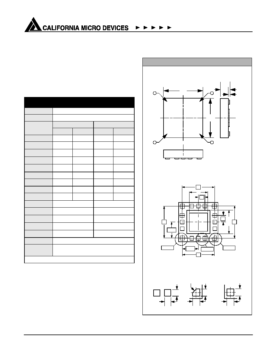
Mechanical Details
The CM2400-01HB is available in a 16-pin HBCC
package.
HBCC16 Mechanical Specifications
Dimensions for CM2400-01HB devices packaged in
16-pin HBCC packages are presented below.
* This is an approximate number which may vary.
Dimensions for HBCC16 Package
PACKAGE DIMENSIONS
Package
HBCC16
Pins
16
Dimensions
Millimeters
Inches
Min
Max
Min
Max
A
-
0.80
0.0315
A
1
0.05
0.10
0.0039
b
1
0.25
0.35
0.0138
b
2
0.30
0.40
0.0157
b
3
0.30
0.40
0.0157
D
2.90
3.10
0.1220
D
h
1.45
1.55
0.0610
E
2.90
3.10
0.1220
E
h
1.75
1.85
0.0728
e
0.50 TYP.
0.0197 TYP.
e
1
2.50 TYP.
0.0984 TYP.
e
2
2.50 TYP.
0.0984 TYP.
e
3
2.45 TYP.
0.0965 TYP.
e
4
2.45 TYP
0.0965 TYP.
# per tube
120 pieces*
# per tape
and reel
2500 pieces
Controlling dimension: millimeters
b
1
b
1
Detail A
Mechanical Package Diagrams
BOTTOM VIEW
TOP VIEW
SIDE VIEW
CONTACT (PIN) DIMENSIONS
b
3
b
3
b
2
CF#0.20x45
b
2
Detail C
Detail B
E
D
5
9
1
13
A
A
1
e
2
E
h
e
D
h
e
3
e
1/2
e
4
1/2
e
3
5
1
13
9
16
e
4
Detail B
e
1
Detail C
Detail A