
«
PGA102
1
PGA102
FEATURES
q
DIGITALLY PROGRAMMABLE GAIN:
G = 1, 10, 100
q
LOW GAIN ERROR: 0.025% max
q
FAST SETTLING: 2.8
Á
s to 0.01%
q
16-PIN PLASTIC AND CERAMIC DIP
APPLICATIONS
q
DATA ACQUISITION AMPLIFIER
q
FIXED-GAIN AMPLIFIER
q
AUTOMATIC GAIN SCALING
DESCRIPTION
The PGA102 is a high speed, digitally programmable-
gain amplifier. CMOS/TTL-compatible inputs select
gains of 1, 10 or 100V/V. Each gain has an indepen-
dent input terminal, providing an input multiplexer
function.
On-chip metal film gain-set resistors are laser-trimmed
to provide excellent gain accuracy. High speed input
circuitry allows multiplexing of high speed signals.
The PGA102 is available in 16-pin plastic and ceramic
DIP packages. Commercial, industrial and military
temperature range models are available.
High Speed
PROGRAMMABLE GAIN AMPLIFIER
V
IN2
1.2k
10.8k
1.33k
10.8k
1.2k
10.8k
Gain/Channel
Select
PGA102
Gain Adj.
V
IN1
Common
Force
Common
Sense
Gain Adj.
V
IN3
4
5
6
10
7
9
8
şV
CC
13
+V
CC
16
Logic
Ground
X10
Select
1
X100
Select
2
Offset
Adjust
11
12
V
OUT
15
3
«
International Airport Industrial Park Ě Mailing Address: PO Box 11400 Ě Tucson, AZ 85734 Ě Street Address: 6730 S. Tucson Blvd. Ě Tucson, AZ 85706
Tel: (520) 746-1111 Ě Twx: 910-952-1111 Ě Cable: BBRCORP Ě Telex: 066-6491 Ě FAX: (520) 889-1510 Ě Immediate Product Info: (800) 548-6132
ę
1985 Burr-Brown Corporation
PDS-579C
Printed in U.S.A. September, 1993

«
PGA102
2
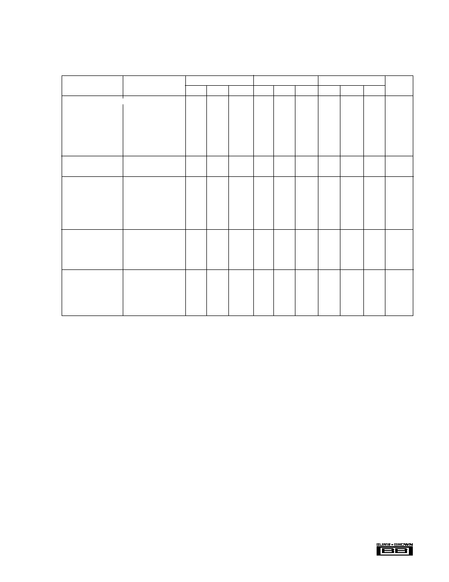
SPECIFICATIONS
ELECTRICAL
At +25
░
C,
▒
V
CC
= 15VDC unless otherwise specified.
GAIN
Inaccuracy
(1)
R
L
= 2k
, G = 1
▒
0.007
▒
0.02
▒
0.003
▒
0.01
*
*
%
G = 10
▒
0.015
▒
0.03
▒
0.01
▒
0.02
*
▒
0.05
%
G = 100
▒
0.02
▒
0.05
▒
0.015
▒
0.025
*
▒
0.06
%
vs Temperature
G = 1
▒
0.4
▒
5
*
*
*
*
ppm/
░
C
G = 10
▒
2
▒
7
*
*
*
*
ppm/
░
C
G = 100
▒
7
▒
20
*
*
▒
9
*
ppm/
░
C
Nonlinearity
R
L
= 2k
, G = 1
0.001
0.003
*
*
*
*
% of FS
G = 10
0.002
0.005
*
*
*
*
% of FS
G = 100
0.003
0.01
*
*
*
*
% of FS
RATED OUTPUT
Voltage
R
L
= 2k
▒
10
▒
12.5
*
*
*
*
V
Current
V
OUT
= 10V
▒
5
▒
10
*
*
*
*
mA
Short Circuit Current
▒
10
▒
25
*
*
*
*
mA
Output Resistance
0.01
*
*
Load Capacitance
For Stable Operation
2000
*
*
pF
INPUT OFFSET VOLTAGE
Initial
(2)
G = 1
▒
200
▒
500
▒
100
▒
250
*
▒
1500
Á
V
G = 10
▒
70
▒
200
▒
50
▒
100
*
▒
600
Á
V
G = 100
▒
70
▒
200
▒
50
▒
100
*
▒
600
Á
V
vs Temperature
G = 1
▒
5
▒
20
*
*
▒
7
▒
50
Á
V/
░
C
G = 10
▒
1
▒
7
*
*
▒
3
▒
10
Á
V/
░
C
G = 100
▒
0.5
▒
3
*
*
▒
2
▒
7
Á
V/
░
C
vs Supply Voltage
▒
5 < V
CC
<
▒
18V
G = 1
▒
30
▒
70
*
*
*
*
Á
V/V
G = 10
▒
8
▒
30
*
*
*
*
Á
V/V
G = 100
▒
8
▒
30
*
*
*
*
Á
V/V
INPUT BIAS CURRENT
Initial
T
A
= +25
░
C
▒
20
▒
50
*
*
*
*
nA
Over Temperature
T
A MIN
to T
A MAX
▒
25
▒
60
*
*
*
*
nA
ANALOG INPUT
CHARACTERISTICS
Voltage Range
Linear Operation
▒
10
▒
12
*
*
*
*
V
Resistance
7 X 10
8
*
*
Capacitance
4
*
*
pF
INPUT NOISE
Voltage Noise
f
B
= 0.1Hz to 10Hz
G = 1
4.5
*
*
Á
Vp-p
G = 10
1.5
*
*
Á
Vp-p
G = 100
0.6
*
*
Á
Vp-p
Voltage Noise Density
f
O
= 1Hz, G = 1
490
*
*
nV/
Hz
G = 10
178
*
*
nV/
Hz
G = 100
83
*
*
nV/
Hz
f
O
= 10Hz, G = 1
155
*
*
nV/
Hz
G = 10
56
*
*
nV/
Hz
G = 100
20
*
*
nV/
Hz
f
O
= 100Hz, G = 1
93
*
*
nV/
Hz
G = 100
31
*
*
nV/
Hz
G = 100
18
*
*
nV/
Hz
f
O
= 1kHz, G = 1
79
*
*
nV/
Hz
G = 10
31
*
*
nV/
Hz
G = 100
18
*
*
nV/
Hz
Current Noise
f
B
= 0.1Hz to 10Hz
76
*
*
pAp-p
Current Noise Density
f
O
= 1Hz
8.8
*
*
pA/
Hz
f
O
= 10Hz
2.8
*
*
pA/
Hz
f
O
= 100Hz
0.99
*
*
pA/
Hz
f
O
= 1kHz
0.43
*
*
pA/
Hz
DYNAMIC RESPONSE
▒
3dB Bandwidth
Small Signal, G = 1
1500
*
*
kHz
G = 10
750
*
*
kHz
G = 100
250
*
*
kHz
Full Power Bandwidth
V
OUT
=
▒
10V, R
L
= 2k
160
*
*
kHz
Slew Rate
V
OUT
=
▒
10V Step,
R
L
= 2k
6
9
*
*
*
*
V/
Á
s
PGA102AG
PGA102BG, SG
PGA102KP
PARAMETER
CONDITIONS
MIN
TYP
MAX
MIN
TYP
MAX
MIN
TYP
MAX
UNITS
«
PGA102
3
PGA102AG
PGA102BG
PGA102KP
PARAMETER
CONDITIONS
MIN
TYP
MAX
MIN
TYP
MAX
MIN
TYP
MAX
UNITS
SPECIFICATIONS
(CONT)
ELECTRICAL
At +25
░
C,
▒
V
CC
= 15VDC unless otherwise specified.
The information provided herein is believed to be reliable; however, BURR-BROWN assumes no responsibility for inaccuracies or omissions. BURR-BROWN assumes
no responsibility for the use of this information, and all use of such information shall be entirely at the user's own risk. Prices and specifications are subject to change
without notice. No patent rights or licenses to any of the circuits described herein are implied or granted to any third party. BURR-BROWN does not authorize or warrant
any BURR-BROWN product for use in life support devices and/or systems.
DYNAMIC RESPONSE (CONT)
Settling Time (0.1%)
V
OUT
= 10V Step, G = 1
1.6
*
*
Á
s
G = 10
2.2
*
*
Á
s
G = 100
5.2
*
*
Á
s
Settling Time (0.01%)
V
OUT
= 10V Step, G = 1
2.8
*
*
Á
s
G = 10
2.8
*
*
Á
s
G = 100
8.2
*
*
Á
s
Overload Recovery
50% Overdrive, G = 1
2.5
*
*
Á
s
Time, 0.1%
(see Performance Curve)
CROSSTALK
DC
▒
10V to Both Off Channels
ş155
*
*
dB
60Hz
▒
10V to Both Off Channels
ş144
*
*
dB
DIGITAL INPUT
CHARACTERISTICS
Input "Low" Threshold
V
IL
(3)
on Pin 1 or 2
VLTC+0.8
*
*
V
Input "Low" Current
1
*
*
Á
A
Input "High" Threshold
V
IH
(3)
on Pin 1 or 2
VLTC+2
1
*
*
*
*
V
Input "High" Current
0.1
1
*
*
*
*
Á
A
Logic Threshold Control
VLTC on Pin 3
şV
CC
V
CC
ş 4
*
*
*
*
V
Switching Time
(4)
Between Channels
1
*
*
Á
s
POWER SUPPLY
Rated Voltage
▒
15
*
*
VDC
Voltage Range
▒
5
▒
18
*
*
*
*
VDC
Quiescent Current
V
OUT
= 0V
▒
2.4
▒
3.3
*
*
*
*
mA
No External Load,
V
OUT
=
▒
10V
▒
5.3
*
*
mA
TEMPERATURE RANGE
Specification, KP Grade
T
A MIN
to T
A MAX
0
+70
░
C
AG and BG Grades
ş25
+85
*
*
░
C
SG Grade
ş55
+125
░
C
Operating
ş55
+125
*
*
ş25
+85
░
C
Storage
ş65
+150
*
*
ş55
+125
░
C
Thermal Resistance
JA
100
*
*
░
C/W
* Specification same as AG grade.
NOTES: (1) Gain inaccuracy is the percent error between the actual and ideal gain selected. It may be externally adjusted to zero for gains of 10 and 100. (2) Offset
voltage can be adjusted for any one channel. Adjustment affects temperature drift by approximately
▒
0.3
Á
V/
░
C for each 100
Á
V of offset adjusted. (3) Voltage on the
logic threshold control pin, VLTC, adjusts the threshold for "Low" and "High" logic levels. (4) Total time to settle equals switching time plus settling time of the newly
selected gain.

«
PGA102
4
Top View
DIP
PIN CONFIGURATION
X10 Select
X100 Select
Logic Threshold Control
Common Force
Common Sense
V
IN1
(X1)
V
IN2
(X10)
V
IN3
(X100)
+V
CC
V
OUT
NC
(1)
şV
CC
Offset Adjust
Offset Adjust
Gain Adjust (X10)
Gain Adjust (X100)
1
2
3
4
5
6
7
8
16
15
14
13
12
11
10
9
NOTE: (1) No Internal Connection.
Power Supply ....................................................................................
▒
18V
Input Voltage Range: Analog ............................................................
▒
V
CC
Digital ................................. (V
PIN 3
ş 5.6V) to +V
CC
Storage Temperature Range: G Package .................... ş65
░
C to +150
░
C
P Package ..................... ş55
░
C to +125
░
C
Lead Temperature (soldering, 10s) ............................................... +300
░
C
Output Short Circuit Duration .............................. Continuous to Common
Junction Temperature: G Package ............................................... +175
░
C
P Package ................................................ +110
░
C
ABSOLUTE MAXIMUM RATINGS
PACKAGE INFORMATION
PACKAGE DRAWING
MODEL
PACKAGE
NUMBER
(1)
PGA102AG
16-Pin Hermetic DIP
109
PGA102BG
16-Pin Hermetic DIP
109
PGA102SG
16-Pin Hermetic DIP
109
PGA102KP
16-Pin Plastic DIP
180
NOTE: (1) For detailed drawing and dimension table, please see end of data
sheet, or Appendix D of Burr-Brown IC Data Book.
ORDERING INFORMATION
MODEL
PACKAGE
TEMPERATURE RANGE
PGA102AG
16-Pin Hermetic DIP
ş25
░
C to +85
░
C
PGA102BG
16-Pin Hermetic DIP
ş25
░
C to +85
░
C
PGA102SG
16-Pin Hermetic DIP
ş55
░
C to +125
░
C
PGA102KP
16-Pin Plastic DIP
0
░
C to +70
░
C
«
PGA102
5
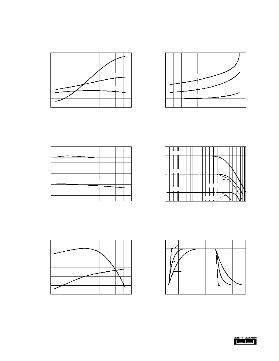
SMALL SIGNAL STEP RESPONSE
Time (Ás)
0
100
0
ş100
G = 1
Output (mV)
2
4
6
8
10
12
G = 10
G =100
SLEW RATE vs TEMPERATURE
Temperature (░C)
Slew Rate (V/Ás)
ş60
13
12
11
10
9
8
7
ş40
0
20
40
60
80
100
120
140
ş20
Negative
Positive
SMALL SIGNAL FREQUENCY RESPONSE
Frequency (Hz)
Gain (dB)
10
50
40
30
20
10
0
ş10
1k
10k
100
100k
1M
10M
G =10
G = 100
G = 1
Large Signal
Large Signal
SETTLING TIME vs TEMPERATURE
Temperature (░C)
Settling Time (Ás)
ş60
10
9
8
7
6
5
4
3
2
1
0
ş40
0
20
40
60
80
100
120
140
ş20
G = 1, 10
G = 100
NONLINEARITY vs TEMPERATURE
Temperature (░C)
Nonlinearity (% FS)
ş60
.006
.005
.004
.003
.002
.001
0
ş40
0
20
40
60
80
100
120
140
ş20
G = 10
G = 100
G = 1
GAIN ERROR vs TEMPERATURE
Temperature (░C)
Gain Error (%)
ş60
0.1
.075
.05
.025
0
ş.025
ş.05
ş40
0
20
40
60
80
100
120
140
ş20
G = 100
G = 10
G = 1
TYPICAL PERFORMANCE CURVES
T
A
= +25
░
C,
▒
V
CC
= 15VDC unless otherwise noted.