
DRV1100
®
In+
In
Out+
+5V
G = 3V/V
DRV1100
Patent
Pending
GND
Out
4
4
Protection
1:4
Transformer
135
HIGH POWER DIFFERENTIAL DRIVER AMPLIFIER
OPA658
DRV1100
DRV1100
International Airport Industrial Park · Mailing Address: PO Box 11400, Tucson, AZ 85734 · Street Address: 6730 S. Tucson Blvd., Tucson, AZ 85706 · Tel: (520) 746-1111 · Twx: 910-952-1111
Internet: http://www.burr-brown.com/ · FAXLine: (800) 548-6133 (US/Canada Only) · Cable: BBRCORP · Telex: 066-6491 · FAX: (520) 889-1510 · Immediate Product Info: (800) 548-6132
DESCRIPTION
The DRV1100 is fixed gain differential line driver
designed for very low harmonic distortion at the high
powers required of xDSL line interface standards.
Operating on a single +5V supply, it can deliver
230mA peak output current and 9.5Vp-p differential
output voltage swing. This high output power on a
single +5V supply makes the DRV1100 an excellent
choice for the xDSL applications that require up to
17dBm power onto the line with high crest factors.
The DRV1100 is available in both 8-pin plastic DIP
and SO-8 packages.
FEATURES
q
HIGH OUTPUT CURRENT: 230mA
q
SINGLE SUPPLY OPERATION: 5V
q
5MHz BANDWIDTH: 6Vp-p into 15
q
VERY LOW THD AT HIGH POWER:
72dBc at 6Vp-p, 100kHz, 100
q
LOW QUIESCENT CURRENT: 11mA
q
FIXED DIFFERENTIAL GAIN: 3V/V
APPLICATIONS
q
xDSL TWISTED PAIR LINE DRIVER
q
COMMUNICATIONS LINE DRIVER
q
TRANSFORMER DRIVER
q
SOLENOID DRIVER
q
HIGH POWER AUDIO DRIVER
q
CRT YOKE DRIVER
©
1996 Burr-Brown Corporation
PDS-1354
Printed in U.S.A. December, 1996
2
®
DRV1100
DRV1100P, U
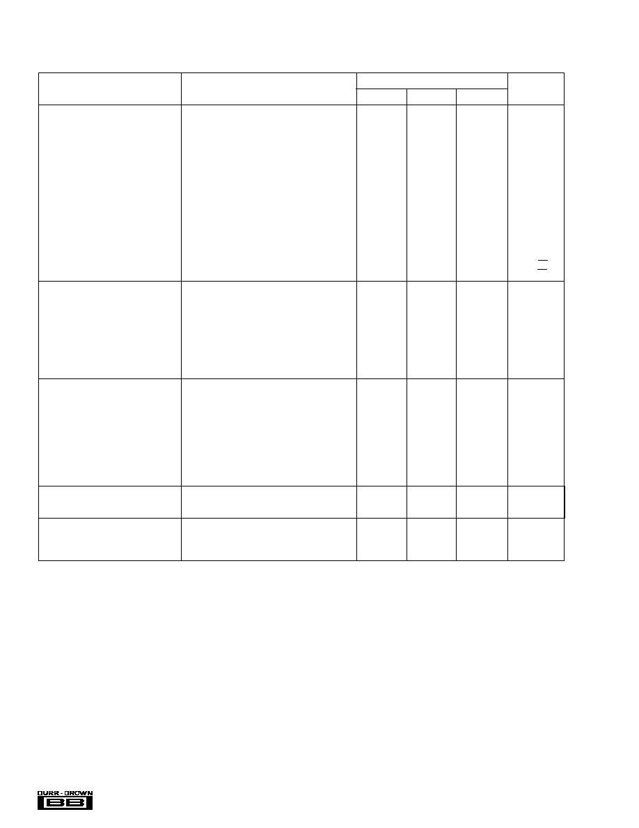
PARAMETER
CONDITIONS
MIN
TYP
MAX
UNITS
AC PERFORMANCE
3dB Bandwidth
R
L
= 15
, V
O
= 1Vp-p
8
MHz
R
L
100
, V
O
= 1Vp-p
11
MHz
R
L
= 15
, V
O
= 6Vp-p
5
MHz
R
L
100
, V
O
= 6Vp-p
6
MHz
Differential Slew Rate
R
L
= 100
, V
O
= 6Vp-p
80
V/
µ
s
Step Response Delay
(1)
V
O
= 1Vp-p
25
ns
Settling Time to 1%, Step Input
V
O
= 1Vp-p, R
L
= 100
0.25
µ
s
Settling Time to 1%, Step Input
V
O
= 6Vp-p, R
L
= 100
0.3
µ
s
Settling Time to 0.1%, Step Input
V
O
= 1Vp-p, R
L
= 100
0.8
µ
s
Settling Time to 0.1%, Step Input
V
O
= 6Vp-p, R
L
= 100
1.1
µ
s
THD, Total Harmonic Distortion
(2)
f = 10kHz
R
L
= 100
, V
O
= 6Vp-p
85
dBc
f = 10kHz
R
L
= 15
, V
O
= 6Vp-p
66
76
dBc
f = 100kHz
R
L
= 100
, V
O
= 6Vp-p
72
dBc
f = 100kHz
R
L
= 15
, V
O
= 6Vp-p
65
dBc
Input Voltage Noise
f = 100kHz
30
nV/
Hz
Input Current Noise
f = 100kHz
0.5
fA/
Hz
INPUT CHARACTERISTICS
Differential Input Resistance
10
11
Differential Input Capacitance
1
pF
Common-Mode Input Resistance
10
11
Common-Mode Input Capacitance
6
pF
Input Offset Voltage
5
mV
Input Bias Current
1
pA
Common-Mode Rejection Ratio
Input Referred
62
dB
Power Supply Rejection Ratio
Input Referred
60
76
dB
Input Common-Mode Voltage Range
(3)
0.5
V
DD
0.5
V
OUTPUT CHARACTERISTICS
Differential Output Offset, RTO
10
25
mV
Differential Output Offset Drift, RTO
40
°
C to +85
°
C
30
µ
V/
°
C
Differential Output Resistance
0.16
Peak Current (Continuous)
R
L
= 15
200
230
mA
Differential Output Voltage Swing
R
L
= 1k
9.6
Vp-p
R
L
= 100
8.5
9.5
Vp-p
R
L
= 15
6.0
6.6
Vp-p
Output Voltage Swing, Each Side
R
L
= 1k
0.125
4.875
V
Gain
Fixed Gain, Differential
3
V/V
Gain Error
±
0.25
dB
POWER SUPPLY
Operating Voltage Range
+4.5
+5.0
+5.5
V
Quiescent Current
V
DD
= 5.0V
+11
+16
mA
TEMPERATURE RANGE
40
+85
°
C
Thermal Resistance,
JA
DRV1100P
8-Pin DIP
100
°
C/W
DRV1100U
8-Pin SO-8
125
°
C/W
NOTES: (1) Time from 50% point of input step to 50% point of output step. (2) Measurement Bandwidth = 500kHz. (3) Output common-mode voltage follows input
common-mode voltage; therefore, if input V
CM
= V
DD
/2, then output V
CM
= V
DD
/2.
SPECIFICATIONS
At V
DD
= +5.0V, V
CM
= V
DD
/2, T
A
= 25
°
C, unless otherwise specified.
The information provided herein is believed to be reliable; however, BURR-BROWN assumes no responsibility for inaccuracies or omissions. BURR-BROWN
assumes no responsibility for the use of this information, and all use of such information shall be entirely at the user's own risk. Prices and specifications are subject
to change without notice. No patent rights or licenses to any of the circuits described herein are implied or granted to any third party. BURR-BROWN does not
authorize or warrant any BURR-BROWN product for use in life support devices and/or systems.

3
®
DRV1100
PIN CONFIGURATIONS
Top View
Analog Inputs: Current ..............................................
±
100mA, Momentary
±
10mA, Continuous
Voltage ....................................... GND 0.3V to V
DD
+0.2V
Analog Outputs Short Circuit to Ground (+25
°
C) ..................... Momentary
Analog Outputs Short Circuit to V
DD
(+25
°
C) ........................... Momentary
V
DD
to GND .............................................................................. 0.3V to 6V
Junction Temperature ................................................................... +150
°
C
Storage Temperature Range .......................................... 40
°
C to +125
°
C
Lead Temperature (soldering, 3s) ................................................. +260
°
C
Power Dissipation .............................. (See Thermal/Analysis Discussion)
ABSOLUTE MAXIMUM RATINGS
In+
2
6
7
4
1
3
5
8
In
Out+
+5V
GND
Out
PACKAGE/ORDERING INFORMATION
PACKAGE DRAWING
PRODUCT
PACKAGE
NUMBER
(1)
DRV1100P
8-Pin PDIP
006
DRV1100U
8-Lead SO-8
182
NOTE: (1) For detailed drawing and dimension table, please see end of data
sheet, or Appendix C of Burr-Brown IC Data Book.
ELECTROSTATIC
DISCHARGE SENSITIVITY
This integrated circuit can be damaged by ESD. Burr-Brown
recommends that all integrated circuits be handled with
appropriate precautions. Failure to observe proper handling
and installation procedures can cause damage.
ESD damage can range from subtle performance degradation
to complete device failure. Precision integrated circuits may
be more susceptible to damage because very small parametric
changes could cause the device not to meet its published
specifications.
GND
In+
In
GND
Out
V
DD
(+5V)
V
DD
(+5V)
Out+
1
2
3
4
8
7
6
5
4
®
DRV1100
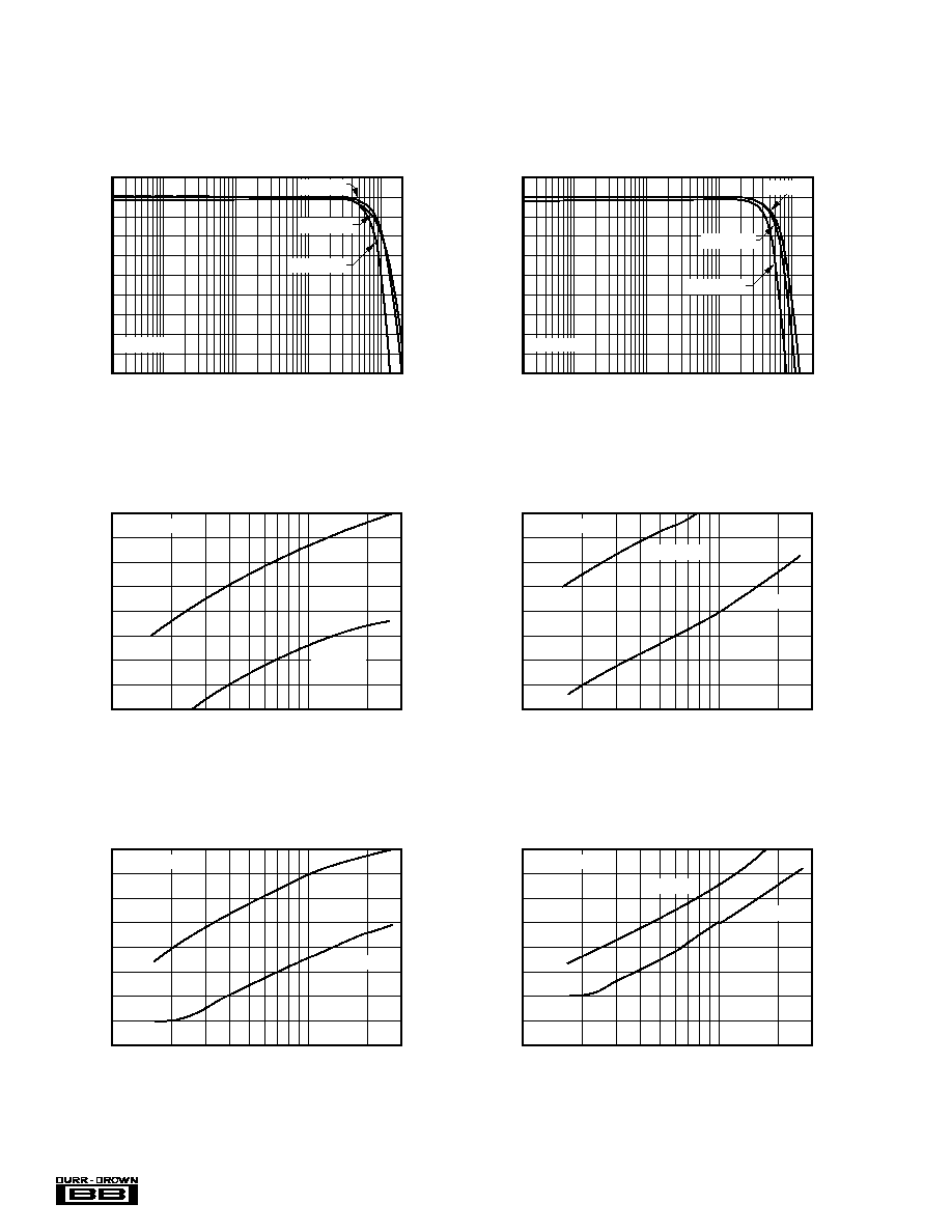
TYPICAL PERFORMANCE CURVES
At V
DD
= +5.0V, V
CM
= V
DD
/2, T
A
= 25
°
C, unless otherwise specified.
40
45
50
55
60
65
70
75
80
100K
SMALL SIGNAL 2ND HARMONIC DISTORTION
2nd Harmonic (dB)
Frequency (Hz)
1M
10M
R
L
= 15
V
O
= 1Vp-p
R
L
= 100
40
45
50
55
60
65
70
75
80
100K
SMALL SIGNAL 3RD HARMONIC DISTORTION
3rd Harmonic (dB)
Frequency (Hz)
1M
10M
V
O
= 1Vp-p
R
L
= 100
R
L
= 15
40
45
50
55
60
65
70
75
80
100K
LARGE SIGNAL 2ND HARMONIC DISTORTION
2nd Harmonic (dB)
Frequency (Hz)
1M
10M
R
L
= 15
V
O
= 6Vp-p
R
L
= 100
40
45
50
55
60
65
70
75
80
100K
LARGE SIGNAL 3RD HARMONIC DISTORTION
3rd Harmonic (dB)
Frequency (Hz)
1M
10M
V
O
= 6Vp-p
R
L
= 100
R
L
= 15
9.5
8.5
7.5
6.5
5.5
4.5
3.5
2.5
1.5
10K
100K
SMALL SIGNAL FREQUENCY RESPONSE
Differential Gain (dB)
Frequency (Hz)
1M
10M
R
L
= 1k
R
L
= 100
R
L
= 15
V
O
= 1Vp-p
9.5
8.5
7.5
6.5
5.5
4.5
3.5
2.5
1.5
10K
100K
LARGE SIGNAL FREQUENCY RESPONSE
Differential Gain (dB)
Frequency (Hz)
1M
10M
R
L
= 1k
R
L
= 100
R
L
= 15
V
O
= 6Vp-p
5
®
DRV1100
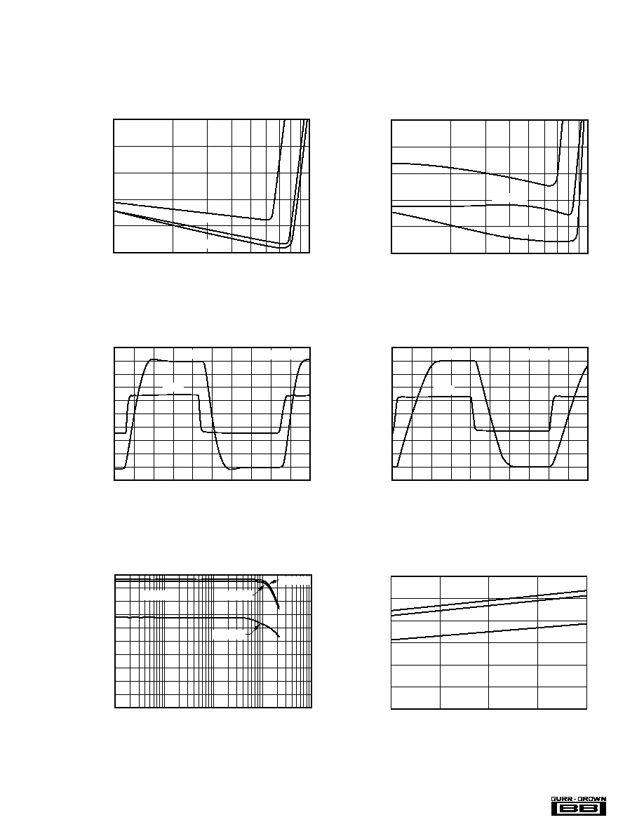
TYPICAL PERFORMANCE CURVES
(CONT)
At V
DD
= +5.0V, V
CM
= V
DD
/2, T
A
= 25
°
C, unless otherwise specified.
40
50
60
70
80
90
1
2
3
4
10kHz THD
THD (dBc)
Differential Output Voltage (Vp-p)
5
6
7
8 9 10
R
L
= 15
R
L
= 100
R
L
= 1k
40
50
60
70
80
90
1
2
3
4
100kHz THD
THD (dBc)
Differential Output Voltage (Vp-p)
5
6
7
8 9 10
R
L
= 15
R
L
= 100
R
L
= 1k
+0.5V
0
0.5V
SMALL SIGNAL STEP RESPONSE
Differential Voltage (125mV/div)
Time (50ns/div)
Output
Input
R
L
= 100
+3V
0
3V
LARGE SIGNAL STEP RESPONSE
Differential Voltage (750mV/div)
Time (50ns/div)
Output
Input
R
L
= 100
12
10
8
6
4
2
0
MAXIMUM V
O
vs SUPPLY VOLTAGE
Differential Output Voltage (Vp-p)
Supply Voltage (V
DD
)
4.5
4.75
5
5.25
5.5
R
L
= 100
R
L
= 1k
R
L
= 15
10
9
8
7
6
5
4
3
2
1
0
10K
1K
100K
LARGE SIGNAL OPERATING RANGE
Differential Output Swing (Vp-p)
Frequency (Hz)
1M
10M
R
L
= 15
R
L
= 1k
R
L
= 100
1% THD
6
®
DRV1100
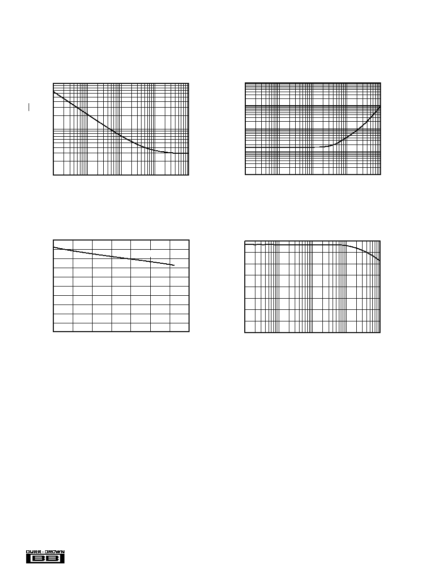
TYPICAL PERFORMANCE CURVES
(CONT)
At V
DD
= +5.0V, V
CM
= V
DD
/2, T
A
= 25
°
C, unless otherwise specified.
1000
100
10
DIFFERENTIAL INPUT VOLTAGE NOISE
Voltage Noise (nV/
Hz)
Frequency (Hz)
100
1K
10K
100K
1M
10
1
0.1
DIFFERENTIAL OUTPUT IMPEDANCE
Impedance (
)
Frequency
1k
10K
100K
1M
10M
13
12
11
10
9
8
7
6
5
4
3
40
20
0
20
40
60
80
100
QUIESCENT CURRENT vs TEMPERATURE
Quiescent Current (mA)
Temperature (°C)
V
DD
= +5V
80
70
60
50
40
30
20
10
0
10K
1K
100K
POWER SUPPLY REJECTION vs FREQUENCY
PSRR (dB)
Frequency (Hz)
1M
10M
7
®
DRV1100
APPLICATIONS INFORMATION
INTERNAL BLOCK DIAGRAM
The DRV1100 is a true differential input to differential
output fixed gain amplifier. Operating on a single +5V
power supply, it provides an internally fixed differential
gain of +3 and a common-mode gain of +1 from the input to
output. Fabricated on an advanced CMOS process, it offers
very high input impedance along with a low impedance
230mA output drive. Figure 1 shows a simplified internal
block diagram.
In+
In
Out+
Out
Buffer
Preamp
FIGURE 1. Simplified DRV1100 Internal Block Diagram.
To achieve the maximum dynamic range, operate the
DRV1100 with the inputs centered at V
DD
/ 2. This will place
the output differential swing centered at V
DD
/ 2 for maxi-
mum swing and lowest distortion. Purely differential input
signals will produce a purely differential output signal. A
single ended input signal, applied to one input of the
DRV1100, with the other input at a fixed voltage, will
produce both a differential and common-mode output signal.
This is an acceptable mode of operation when the DRV1100
is driving an element with good common-mode rejection
(such as a transformer).
DIFFERENTIAL OUTPUT VOLTAGE AND POWER
Applying the balanced differential output voltage of the
DRV1100 to a load between the outputs will produce a peak-
to-peak voltage swing that is twice the swing of each
individual output. This is illustrated in Figure 2 where the
common-mode voltage is V
DD
/ 2. For a load connected
between the outputs, the only voltage that matters is the
differential voltage between the two outputs--the common-
mode voltage does not produce any load current in this case.
The peak power that the DRV1100 can deliver into a
differential load is V
P
2
/ R
L
. The Typical Performance Curves
show the maximum Vp-p versus load and frequency. The
peak voltage (Vp) equals 1/2 of the peak-to-peak voltage
(Vp-p). Squaring 1/2 of the Vp-p and dividing by the load
will give the peak power. For example, the Typical Perfor-
mance Curves show that on +5V supply the DRV1100 will
deliver 6.8Vp-p into 15
at 500kHz. The peak load power
under this condition is (6.8Vp-p/2)
2
/15
= 770mW.
SUPPLY VOLTAGE
The DRV1100 is designed for operation on a single +5V
supply. For loads > 200
, each output will swing rail to rail.
This gives a peak-to-peak differential output swing that is
approximately = 2 · V
DD
. For best distortion performance,
the power supply should be decoupled to a good ground
plane immediately adjacent to the package with a 0.1
µ
F
capacitor. In addition, a larger electolytic supply decoupling
capacitor (6.8
µ
F) should be near the package but can be
shared among multiple devices.
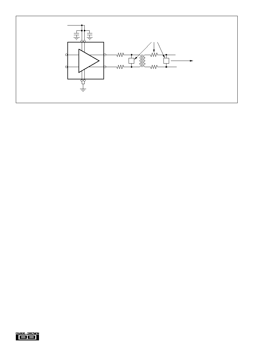
DIGITAL SUBSCRIBER LINE APPLICATIONS
The DRV1100 is particularly suited to the high power, low
distortion, requirements of a twisted pair driver in digital
communications applications. These include HDSL (High
bit rate Digital Subscriber Lines), ADSL (Asymmetrical
Digital Subscriber Lines), and RADSL (Rate adaptive ADSL).
Figure 3 shows a typical transformer coupled xDSL line
driver configuration. In general, the DRV1100 is usable for
output power requirements up to 17dBm with a crest factor
up to 6 (crest factor is the ratio of peak to rms voltage).
To calculate the required amplifier power for an xDSL
application--
· Determine the average power required onto the line in the
particular application. The DRV1100 must be able to
deliver twice this power (+3dB) to account for the power
FIGURE 2. DRV1100 Single Ended and Differential Output
Waveforms.
Out+
V
DD
/2
Out
V
DD
/2
Load
0V
V
P
V
P
V
P
V
P
8
®
DRV1100
loss through the series impedance matching resistors shown
in Figure 3. Twice the required line power must be
delivered by the DRV1100 through the frequency band
of interest with the distortion required by the system.
· Calculate the RMS voltage required at the output of the
DRV1100 with this 2X line power requirement. Vrms =
(2 · P
LINE
· R
L
)
1/2
, where R
L
is the total load impedance
that the DRV1100 must drive. Multiply this Vrms by 2 ·
crest factor to get the total required differential peak-to-
peak voltage at the output. The DRV1100 must be able
to drive the peak-to-peak differential voltage into the
load impedance.
Where possible, the transformer turns ratio may be adjusted
to keep within the DRV1100 output voltage and current
constraints for a given R
LINE
and desired power onto the
line.
Using the example of Figure 3, assume the average power
desired on a 135
line is 14dBm (HDSL). Twice this power
(17dBm) is required into the matching resistors on the
primary side of the transformer. This 135
load is reflected
through the 1:4 transformer as a (135/(4
2
)) = 8.4
load. The
two series 4.1
resistors, along with the 0.2
differential
output impedance of the DRV1100, will provide impedance
matching into this 8.4
load. The DRV1100 will see ap-
proximately a 16.5
load under these conditions. The re-
quired 17dBm (50mW) into this load will need an output
Vrms = (50mW · 16.5)
1/2
= 0.91Vrms. Assuming a crest
factor of 3, the differential peak-to-peak output voltage = 6
· 0.91 = 5.45Vp-p. The Typical Performance Curves show
that, at 100kHz, the DRV1100 can deliver this voltage swing
with less than 62dB THD.
OUTPUT PROTECTION
Figure 3 also shows overvoltage and short circuit protection
elements that are commonly included in xDSL applications.
Overvoltage suppressors include diodes or MOV's. The
outputs of the DRV1100 can be momentarily shorted to
In+
In
Out+
+5V
DRV1100
GND
Out
4
4
Protection Circuits
1:4
Transformer
Line Impedance
135
FIGURE 3. Typical Digital Subscriber Line Application.
ground or to the supply without damage. The outputs are not,
however, designed for a continuous short to ground or the
supply.
POWER DISSIPATION AND THERMAL ANALYSIS
The total internal power dissipation of the DRV1100 is the
sum of a quiescent term and the power dissipated internally
to deliver the load power. The Typical Performance Curves
show the quiescent current over temperature. At +5V sup-
ply, the typical no load supply current of 11mA will dissi-
pate 55mW quiescent power. The rms power dissipated in
the output circuit to deliver a Vrms to a load R
L
is:
Prms = (V
DD
Vrms) · (Vrms/R
L
)
The internal power dissipation will reach a maximum when
Vrms is equal to V
DD
/ 2. For a sinusoidal output, this
corresponds to an output Vp-p = 1.41 · V
DD
.
As an example, compute the power and junction temperature
under a worst case condition with V
DD
= +5V and Vrms =
2.5V into a 16
differential load (peak output current for a
sinusoid would be 222mA). The total internal power dissi-
pation would be:
(5V · 11mA) + (5V 2.5V) · (2.5V/16
) = 446mW
To compute the internal junctions temperature, this power is
multiplied by the junction to ambient thermal impedance (to
get the temperature rise above ambient) then added to the
ambient temperature. Using the specified maximum ambient
temperature of +85
°
C, the junction temperature for the
DRV1100 in an SO-8 package under these worst case
conditions will be:
T
J
= 85
°
C + 0.446W · 125
°
C/W = 141
°
C
9
®
DRV1100
90
80
70
60
50
40
30
20
10
0
0
0.5
1
1.5
INTERNAL TEMPERATURE RISE
OF DRV1100 IN SOIC
Temperature Rise
Load Voltage (rms)
2
2.5
3
3.5
R
L
= 15
Limit at 85°C Ambient
R
L
= 100
Often, the R
B
resistors will be set to a relatively high value
(> 10k
) to minimize quiescent current in the reference
path. If a lower input impedance is desired, additional
terminating resistors may be added to the input side of the
blocking capacitors (C
B
).
The circuit of Figure 5 may also be operated with only a
single ended input. In that case, the reference voltage on the
other input should be decoupled to ground with a 0.1
µ
F
capacitor. In this connection, the input will generate unbal-
anced outputs. The differential output voltage will still be
3 times the input peak-to-peak voltage, but since there is
now a common-mode voltage input, there will be a common
mode voltage output. The output common-mode voltage
will be equal to the input signal's peak-to-peak swing. This
common-mode component will reduce the available differ-
ential output voltage swing. However, if the output load has
good common-mode rejection, such as a transformer, this is
an acceptable way of using the DRV1100 with a single
ended source.
Figure 6 shows a means of translating a ground centered
single ended input to a purely differential signal for applica-
tion to DRV1100 input. This circuit uses a wideband dual op
amp in cross coupled feedback configuration.
The outputs of this circuit may then be fed into the inputs of
Figure 5. The total gain of Figure 6 is 2 · (R
F
/ R
G
). The
circuit will act to hold all 4 op amp inputs equal to the
+ input of the lower op amp. Since this is at ground, the
midpoint for the input signal (where the two outputs will be
equal) is also at 0V.
FIGURE 5. AC Coupled Differential Input Interface.
DRV1100
R
L
R
B
C
B
C
B
+V
DD
V
1
V
2
R
B
R
B
R
B
FIGURE 4. Junction Temperature Rise From Ambient for
the DRV1100U.
The internal junction temperature should, in all cases, be
limited to < 150
°
C. For a maximum ambient temperature of
+85
°
C, this limits the internal temperature rise to less than
65
°
C. Figure 4 shows the temperature rise from ambient to
junction for loads of 15
and 100
. This shows that the
internal junction temperature will never exceed the rated
maximum for a 15
load.
INPUT INTERFACE CIRCUITS
Best performance with the DRV1100 is achieved with a
differential input centered at V
DD
/2. Signals that do not
require DC coupling may be connected as shown in Figure
5 through blocking caps to a midpoint reference developed
through resistor dividers from the supply voltage. The value
for the R
B
resistors determine four performance require-
ments.
· They bias the inputs at the supply midpoint.
· They provide a DC bias current path for the input to the
DRV1100
· They set the AC input impedance for the source signals to
R
B
/2.
· They set the low frequency cutoff frequency along with
C
B
.
1/2
OPA2650
V
I
R
F
R
G
500
500
500
+ V
I
R
F
R
G
1/2
OPA2650
500
V
I
R
F
R
G
FIGURE 6. Single Ended to Differential Conversion.