Û
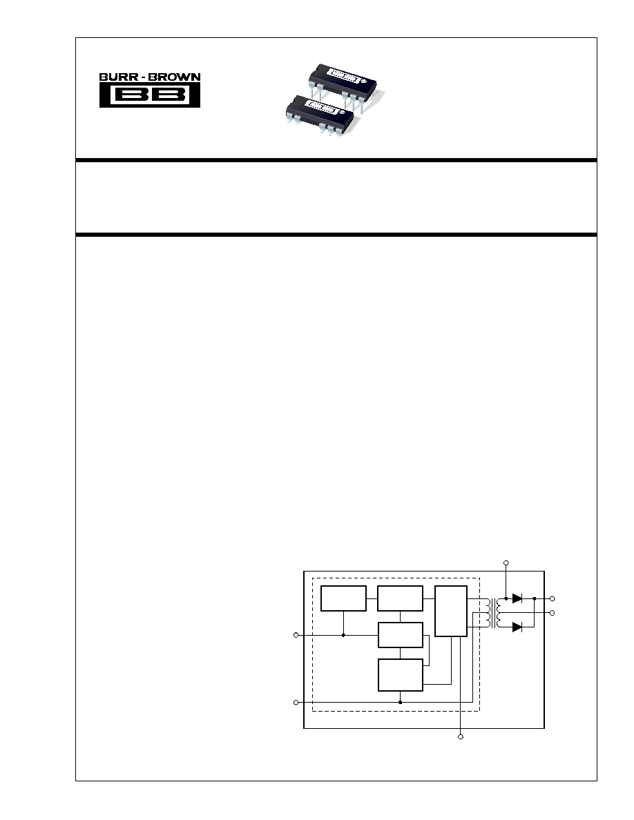
Miniature 5V Input, 1W Isolated
UNREGULATED DC/DC CONVERTERS
FEATURES
q
STANDARD JEDEC PLASTIC PACKAGE
q
MEETS EN55022 CLASS B
q
LOW PROFILE: 0.15" (3.8mm)
q
SYNCHRONIZABLE
q
OUTPUT SHORT CIRCUIT PROTECTION
q
THERMAL SHUTDOWN
q
STARTS INTO ANY CAPACITIVE LOAD
q
FLOATING OUTPUTS
q
EFFICIENCY: Up to 75% (at Full Load)
q
1000Vrms ISOLATION
q
400kHz SWITCHING
q
108 MILLION HOURS MTTF
q
5V,
Ý
5V, 12V,
Ý
12V, 15V,
Ý
15V OUTPUTS
q
AVAILABLE IN TAPE AND REEL
DESCRIPTION
The DCP0105 family is a series of high efficiency, 5V
input isolated DC/DC converters. In addition to 1W
nominal galvanically isolated output power capability,
the range of DC/DCs are also fully synchronizable.
The devices feature thermal shutdown, and overload
protection is implemented via watchdog circuitry.
Advanced power-on reset techniques give superior
reset performance and the devices will start into any
capacitive load up to full power output.
The DCP0105 family is implemented in standard-
molded IC packaging, giving outlines suitable for high
volume assembly.
DCP0105
Series
ternational Airport Industrial Park ñ Mailing Address: PO Box 11400, Tucson, AZ 85734 ñ Street Address: 6730 S. Tucson Blvd., Tucson, AZ 85706 ñ Tel: (520) 746-1111
Twx: 910-952-1111 ñ Internet: http://www.burr-brown.com/ ñ Cable: BBRCORP ñ Telex: 066-6491 ñ FAX: (520) 889-1510 ñ Immediate Product Info: (800) 548-6132
ˋ
1996 Burr-Brown Corporation
PDS-1336G
Printed in U.S.A. May, 1999
APPLICATIONS
q
POINT OF USE POWER CONVERSION
q
DIGITAL INTERFACE POWER
q
GROUND LOOP ELIMINATION
q
DATA ACQUISITION
q
INDUSTRIAL CONTROL AND
INSTRUMENTATION
q
TEST EQUIPMENT
I
BIAS
Power
Stage
V
OUT
¼ 2
Reset
800kHz
Oscillator
Watch-dog/
start-up
PSU
Thermal
Shutdown
SYNC
OUT
SYNC
IN
V
S
0V
Power Controller IC
0V
DCP0105
DCP0105
Û
DCP0105
2
SPECIFICATIONS
At T
A
= +25
¯
C, V
S
= +5V, unless otherwise specified.
DCP0105 SERIES
PARAMETER
CONDITIONS
MIN
TYP
MAX
UNITS
OUTPUT
Power
V
S
+ 4%
1
W
100% Full Load
0.92
W
Voltage (V
NOM
)
DCP010505
75% Full Load
(1)
4.6
5
5.1
V
DCP010505D
75% Full Load
Ý
4.6
Ý
5
Ý
5.1
V
DCP010512
75% Full Load
11.2
12
12.4
V
DCP010512D
75% Full Load
Ý
11.2
Ý
12
Ý
12.4
V
DCP010515
75% Full Load
14.0
15
15.5
V
DCP010515D
75% Full Load
Ý
14.0
Ý
15
Ý
15.5
V
Voltage vs Temperature
Ý
0.08
%/
¯
C
Short-Circuit Duration
V
S
Ý
10%
Indefinite
Ripple
C
L
= O/P Capacitor = 10
ç
F
20
mVp-p
INPUT
Nominal Voltage (V
S
)
5
V
Voltage Range
Ù10
10
%
Supply Current
100% Full Load
250
mA
Reflected Ripple Current
C
IN
= I/P Capacitor = 1
ç
F
20
mArms
50% Full Load
ISOLATION
Voltage
(2)
1s Flash Test
1
kVrms
Continuous Voltage
(3)
1
kVrms
Insulation Resistance
>1
G
Input/Output Capacitance
2.5
pF
LOAD REGULATION
DCP010505
10% to 100% Load
25
31
%
10% to 75% Load
17
%
75% to 100% Load
Ù8
%
DCP010505D
10% to 100% Load
25
32
%
10% to 75% Load
19
%
75% to 100% Load
Ù8
%
DCP010512
10% to 100% Load
17
38
%
10% to 25% Load
7
%
25% to 75% Load
12
%
75% to 100% Load
Ù7
%
DCP010512D
10% to 100% Load
20
37
%
10% to 25% Load
7
%
25% to 75% Load
12
%
75% to 100% Load
Ù7
%
DCP010515
10% to 100% Load
20
42
%
10% to 25% Load
11
%
25% to 75% Load
12
%
75% to 100% Load
Ù7
%
DCP010515D
10% to 100% Load
16
41
%
10% to 25% Load
11
%
25% to 75% Load
12
%
75% to 100% Load
Ù7
%
SWITCHING/SYNCHRONIZATION
Oscillator Frequency (F
OSC
)
Switching Frequency = F
OSC
/2
800
kHz
Sync Input Low
0
0.8
V
Sync Input Current
V
SYNC
= +2V
48
ç
A
Reset Time
3.8
ç
s
SYNC
OUT
Frequency
400
kHz
GENERAL
No Load Current
DCP010505P
0% Full Load
38
mA
DCP010505DP
0% Full Load
40
mA
DCP010512P
0% Full Load
30
mA
DCP010512DP
0% Full Load
33
mA
DCP010515P
0% Full Load
34
mA
DCP010515DP
0% Full Load
34
mA
3
Û
DCP0105
GENERAL (Cont)
Efficiency
DCP010505
100% Full Load
71
%
10% Full Load
40
%
DCP010505D
100% Full Load
66
%
10% Full Load
47
%
DCP010512
100% Full Load
72
%
10% Full Load
38
%
DCP010512D
100% Full Load
72
%
10% Full Load
36
%
DCP010515
100% Full Load
73
%
10% Full Load
40
%
DCP010515D
100% Full Load
75
%
10% Full Load
38
%
MTTF
(3)
T
A
= +85
¯
C
158,000
hrs
T
A
= +55
¯
C
3,050,000
hrs
T
A
= +25
¯
C
108,000,000
hrs
Weight
14-Pin PDIP
1.08
g
THERMAL SHUTDOWN
Internal Controller IC Temperature
115
140
¯
C
Shutdown Current
3
mA
TEMPERATURE RANGE
Operating
Ù40
+100
¯
C
NOTES: (1) 100% load current = 1W/V
NOM
typical. (2) Rated working voltage = 130Vr ms (IEC950 Convention). (3) Life test data.
SPECIFICATIONS
(CONT)
At T
A
= +25
¯
C, V
S
= +5V, unless otherwise specified.
DCP0105 SERIES
PARAMETER
CONDITIONS
MIN
TYP
MAX
UNITS
EMC SPECIFICATIONS
Specifications and Related Documents
The DCP010505 was tested to and complied with the limits of the following EMC specifications:
prEN55022 (1992)
Conducted RF emission, telecomm lines.
EN55022 (1995)
Limits and methods of measurement of radio interference characteristics of information technology equipment.
ENV50140 (1993)
Electromagnetic compatibility. Basic immunity standard. Radiated RF immunity.
ENV50141 (1993)
Electromagnetic compatibility. Basic immunity standard. Conducted RF immunity.
EN61000-4-2 (1995)
Electromagnetic compatibility, Part 4. Testing and measurement techniques, Section 2. Electrostatic
discharge.
EN61000-4-4 (1995)
Electromagnetic compatibility, Part 4. Testing and measurement techniques, Section 4. Electrical fast
transient bursts.
EN61000-4-8 (1994)
Electromagnetic compatibility, Part 4. Testing and measurement techniques, Section 8. Power frequency
magnetic field immunity.
List of Tests
The following is a list of tests which were required for compliance with the above specifications:
Conducted Emission Test
150kHz to 30MHz, power and output lines, Class B limits applying. DC/DC loads of
0%, 8%, and 120% applying.
Radiated Emission Test
30MHz to 1000MHz, Class B limits applying. DC/DC loads of 0%, 8%, and 120%
applying.
Radiated Immunity Test, Electric Field
80MHz to 1000MHz, 10V/m, 1kHz 80% AM.
Radiated Immunity Test, Electric Field
900MHz, 10V/m, 200Hz 100% PM.
Electrostatic Discharge Test
4kV, HCP/VCP indirect discharge only.
Electrical Fast Transient Tests
2kV power lines, 2kV signal lines.
Conducted RF Immunity Tests
150kHz to 80MHz, power and output lines, 10Vrms, 1kHz 80% AM.
Radiated Immunity Test, Magnetic Field
50Hz, 30A/m
Û
DCP0105
4
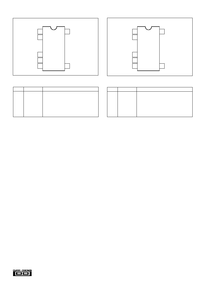
Top View
DIP
PIN CONFIGURATION (Single)
Top View
DIP
PIN CONFIGURATION (Dual)
DCP0105
1
2
5
6
7
14
8
V
S
0V
0V
+V
OUT
ÙV
OUT
SYNC
IN
SYNC
OUT
DCP0105
1
2
5
6
7
14
8
V
S
0V
0V
+V
OUT
NC
SYNC
IN
SYNC
OUT
PIN DEFINITIONS (Single)
PIN #
PIN NAME
DESCRIPTION
1
V
S
Voltage Input.
2
0V
Input Side Common.
5
0V
Output Side Common.
6
+V
OUT
+Voltage Out.
7
NC
Not Connected.
8
SYNC
OUT
Unregulated 400kHz Output from Transformer.
14
SYNC
IN
Synchronization Pin.
PIN DEFINITIONS (Dual)
PIN #
PIN NAME
DESCRIPTION
1
V
S
Voltage Input.
2
0V
Input Side Common.
5
0V
Output Side Common.
6
+V
OUT
+Voltage Out.
7
ÙV
OUT
ÙVoltage Out.
8
SYNC
OUT
Unregulated 400kHz Output from Transformer.
14
SYNC
IN
Synchronization Pin.
The information provided herein is believed to be reliable; however, BURR-BROWN assumes no responsibility for inaccuracies or omissions. BURR-BROWN assumes
no responsibility for the use of this information, and all use of such information shall be entirely at the user's own risk. Prices and specifications are subject to change
without notice. No patent rights or licenses to any of the circuits described herein are implied or granted to any third party. BURR-BROWN does not authorize or warrant
any BURR-BROWN product for use in life support devices and/or systems.
5
Û
DCP0105
Input Voltage .......................................................................................... 7V
Storage Temperature ...................................................... Ù60
¯
C to +150
¯
C
Lead Temperature (soldering, 10s) ................................................. 300
¯
C
ABSOLUTE MAXIMUM RATINGS
DCP01
Basic Model Number: 1W Product
Voltage Input:
5V In
Voltage Output:
5V Out
Dual Output:
Package Code:
P = 14-Pin Plastic DIP
P-U = 14-Pin Plastic DIP Gull Wing
ORDERING INFORMATION
05
05
(
)
( D )
ELECTROSTATIC
DISCHARGE SENSITIVITY
This integrated circuit can be damaged by ESD. Burr-Brown
recommends that all integrated circuits be handled with
appropriate precautions. Failure to observe proper handling
and installation procedures can cause damage.
ESD damage can range from subtle performance degrada-
tion to complete device failure. Precision integrated circuits
may be more susceptible to damage because very small
parametric changes could cause the device not to meet its
published specifications.
PACKAGE
SPECIFIED
DRAWING
TEMPERATURE
PACKAGE
ORDERING
TRANSPORT
PRODUCT
PACKAGE
NUMBER
(1)
RANGE
MARKING
NUMBER
(2)
MEDIA
Single
DCP010505
14-Pin PDIP
010-1
Ù40
¯
C to +100
¯
C
DCP010505P
DCP010505P
Rails
DCP010505
14-Pin PDIP Gull Wing
010-2
Ù40
¯
C to +100
¯
C
DCP010505P-U
DCP010505P-U
Rails
"
"
"
"
"
DCP010505P-U/700
Tape and Reel
DCP010512
14-Pin PDIP
010-1
Ù40
¯
C to +100
¯
C
DCP010512P
DCP010505P
Rails
DCP010512
14-Pin PDIP Gull Wing
010-2
Ù40
¯
C to +100
¯
C
DCP010512P-U
DCP010505P-U
Rails
"
"
"
"
"
DCP010505P-U/700
Tape and Reel
DCP010515
14-Pin PDIP
010-1
Ù40
¯
C to +100
¯
C
DCP010515P
DCP010505P
Rails
DCP010515
14-Pin PDIP Gull Wing
010-2
Ù40
¯
C to +100
¯
C
DCP010515P-U
DCP010505P-U
Rails
"
"
"
"
"
DCP010505P-U/700
Tape and Reel
Dual
DCP010505D
14-Pin PDIP
010-1
Ù40
¯
C to +100
¯
C
DCP010505DP
DCP010505DP
Rails
DCP010505D
14-Pin PDIP Gull Wing
010-2
Ù40
¯
C to +100
¯
C
DCP010505DP-U
DCP010505DP-U
Rails
"
"
"
"
"
DCP010505DP-U/700
Tape and Reel
DCP010512D
14-Pin PDIP
010-1
Ù40
¯
C to +100
¯
C
DCP010512DP
DCP010512DP
Rails
DCP010512D
14-Pin PDIP Gull Wing
010-2
Ù40
¯
C to +100
¯
C
DCP010512DP-U
DCP010512DP-U
Rails
"
"
"
"
"
DCP010512DP-U/700
Tape and Reel
DCP010515D
14-Pin PDIP
010-1
Ù40
¯
C to +100
¯
C
DCP010515DP
DCP010515DP
Rails
DCP010515D
14-Pin PDIP Gull Wing
010-2
Ù40
¯
C to +100
¯
C
DCP010515DP-U
DCP010515DP-U
Rails
"
"
"
"
"
DCP010515DP-U/700
Tape and Reel
NOTES: (1) For detailed drawing and dimension table, please see end of data sheet, or Appendix C of Burr-Brown IC Data Book. (2) Models with a slash (/) are
available only in Tape and Reel in the quantities indicated (e.g., /700 indicates 700 devices per reel). Ordering 700 pieces of DCP010505P-U/700 will get a single
700-piece Tape and Reel. For detailed Tape and Reel mechanical information, refer to Appendix B of Burr-Brown IC Data Book.
PACKAGE/ORDERING INFORMATION
Û
DCP0105
6
0
40
Full Load (%)
Efficiency (%)
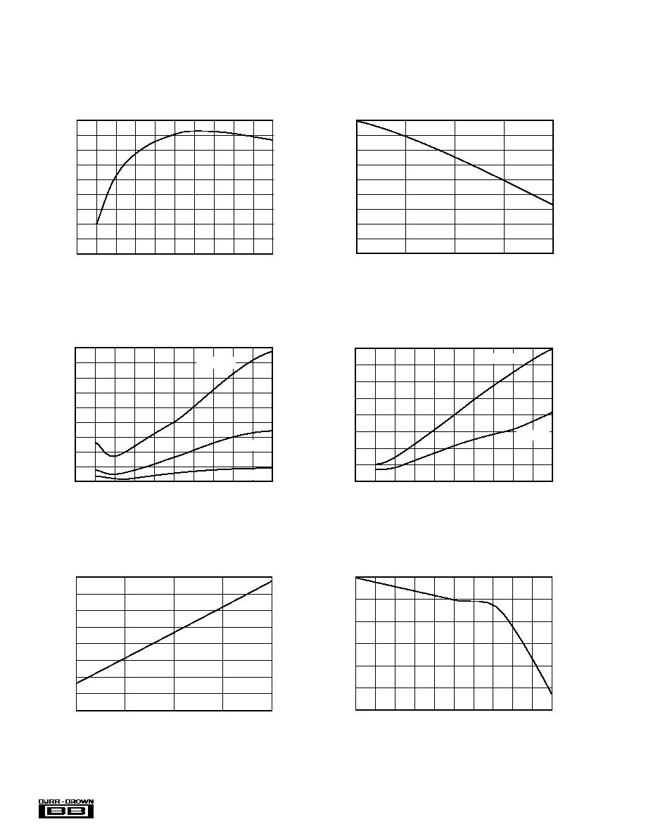
DCP010505 EFFICIENCY vs LOAD
50
60
70
80
90
100
10
20
30
75
70
65
60
55
50
45
40
35
30
TYPICAL PERFORMANCE CURVES
(Common and DCP010505 Specific)
At T
A
= +25
¯
C, V
OUT
nominal (V
NOM
) = +5V and V
S
= +5V, unless otherwise noted.
10
25
50
75
Full Load (%)
Output Voltage (V)
DCP010505 OUTPUT VOLTAGE vs LOAD
100
5.8
5.6
5.4
5.2
5.0
4.8
4.6
4.4
4.2
4
0
40
Load (%)
Peak-to-Peak Ripple Voltage (mV)
PEAK-TO-PEAK RIPPLE VOLTAGE vs LOAD
50
60
70
80
90
100
10
20
30
180
160
140
120
100
80
60
40
20
0
C
L
= 200nF
C
L
= 1çF
C
L
= 10çF
Input (V)
Output Voltage (V)
DCP010505 OUTPUT vs INPUT VOLTAGE (75% Load)
5.6
5.4
5.2
5
4.8
4.6
4.4
4.2
4
4.5
4.75
5
5.25
5.5
4.5
4.9
Input Supply Voltage (V)
Frequency (%)
SWITCHING FREQUENCY vs SUPPLY VOLTAGE
5.0
5.1
5.2
5.3
5.4
5.5
4.6
4.7
4.8
100.0
99.95
99.90
99.85
99.80
99.75
99.70
0
40
Load (%)
rms Ripple Current (mA)
REFLECTED rms RIPPLE CURRENT vs LOAD
50
60
70
80
90
100
10
20
30
80
70
60
50
40
30
20
10
0
C
IN
= 100nF
C
IN
= 1çF
7
Û
DCP0105
0.15
10
1
30
Frequency (MHz)
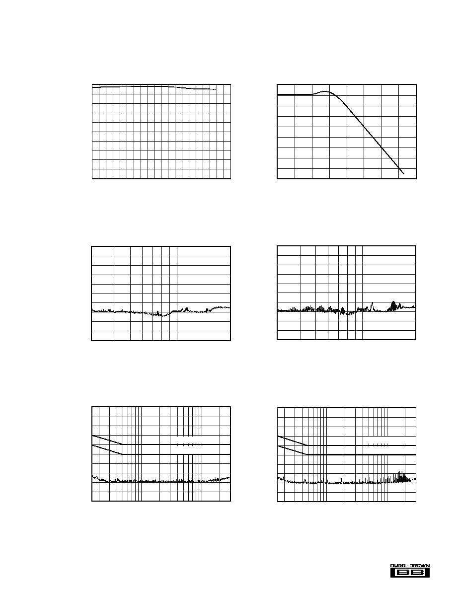
CONDUCTED EMISSIONS (120% Load)
70
50
30
10
Ù10
55022B QP Limit
55022B AV Limit
Emission Level, Peak (dBçA)
0.15
10
1
30
Frequency (MHz)
CONDUCTED EMISSIONS (8% Load)
70
50
30
10
Ù10
55022B QP Limit
55022B AV Limit
Emission Level, Peak (dBçA)
30
100
200
Frequency (MHz)
RADIATED EMISSIONS (120% Load)
90
70
50
30
10
55022B (3m) Limit
Emission Level, Peak (dBçV/m)
TYPICAL PERFORMANCE CURVES
(Common and DCP010505 Specific, cont)
At T
A
= +25
¯
C, V
OUT
nominal (V
NOM
) = +5V and V
S
= +5V, unless otherwise noted.
Ù40
Ù20
0
20
30
50
70
90
100
110
Ù30
Ù10
10
25
40
60
80
95
105
115 120
Temperature (¯C)
Output Power (W)
DCP010505 OUTPUT POWER vs TEMPERATURE
1
0.9
0.8
0.7
0.6
0.5
0.4
0.3
0.2
0.1
0
Ù40
40
Temperature (¯C)
Frequency (%)
SWITCHING FREQUENCY vs TEMPERATURE
60
80
100
120
Ù20
0
20
101
100
99
98
97
96
95
94
93
92
30
100
200
Frequency (MHz)
55022B (3m) Limit
Emission Level, Peak (dBçV/m)
RADIATED EMISSIONS (8% Load)
90
70
50
30
10
Û
DCP0105
8
0
10
20
30
40
50
60
70
80
90
100
Load (%)
Efficiency (%)
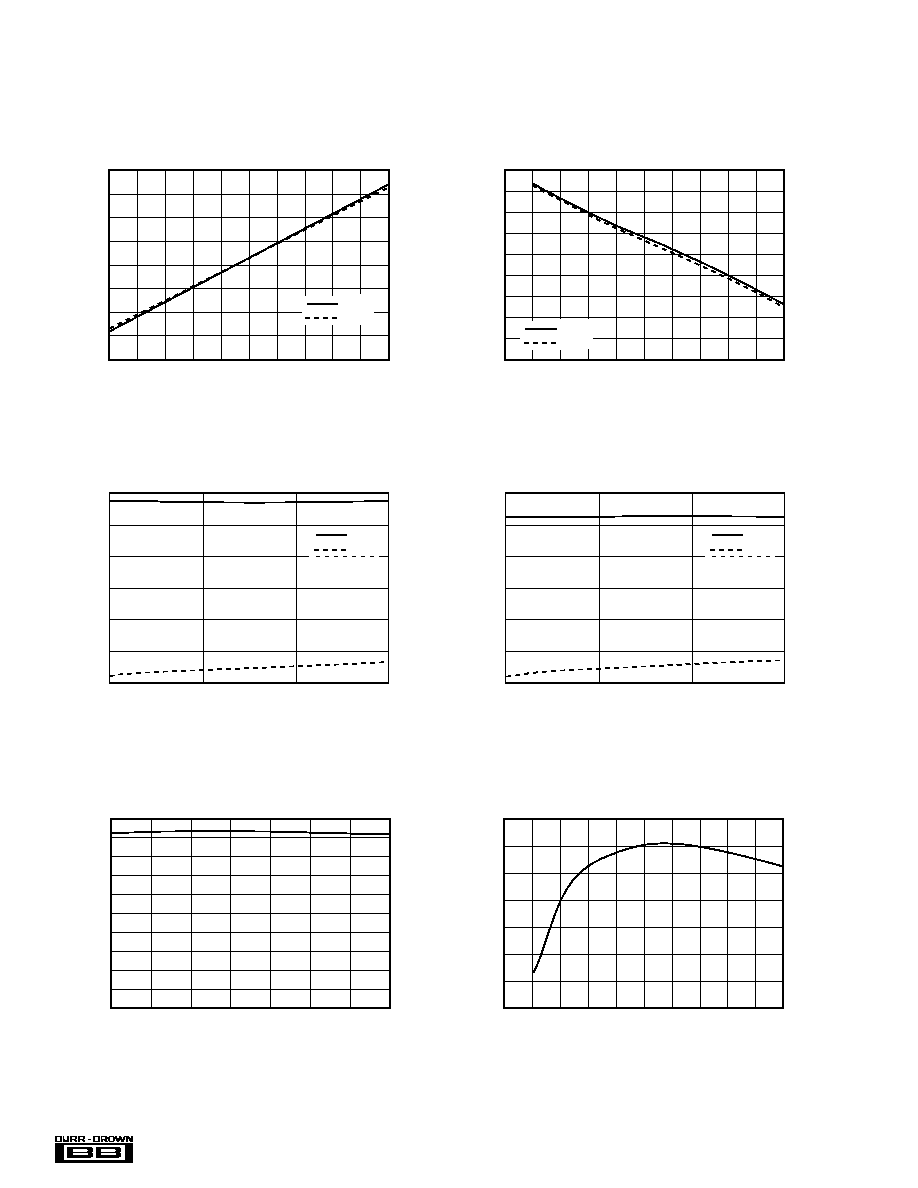
DCP010505D EFFICIENCY vs LOAD
75
70
65
60
55
50
45
40
Ù40
Ù20
0
20
40
60
80
100
Temperature (¯C)
Power Out (W)
DCP010505D POWER vs TEMPERATURE
1
0.9
0.8
0.7
0.6
0.5
0.4
0.3
0.2
0.1
0
10
40
70
100
ÙV
OUT
Load (% of FL)
V
OUT
DCP010505D LOAD BALANCE (+V
OUT
Load = 100%)
6
4
2
0
Ù2
Ù4
Ù6
+V
OUT
ÙV
OUT
10
40
70
100
ÙV
OUT
Load (% of FL)
V
OUT
DCP010505D LOAD BALANCE (+V
OUT
Load = 10%)
6
4
2
0
Ù2
Ù4
Ù6
+V
OUT
ÙV
OUT
0
10
20
30
40
50
70
80
90
60
100
Load (%)
Output Voltage (V)
DCP010505D OUTPUT VOLTAGE vs LOAD
5.80
5.60
5.40
5.20
5.00
4.80
4.60
4.40
4.20
4.00
+V
OUT
ÙV
OUT
4.5
4.6
4.7
4.8
4.9
5.0
5.2
5.3
5.4
5.1
5.5
Input Voltage (V)
Output Voltage (V)
DCP010505D OUTPUT vs INPUT VOLTAGE (75% Load)
5.6
5.4
5.2
5.0
4.8
4.6
4.4
4.2
4.0
+V
OUT
ÙV
OUT
TYPICAL PERFORMANCE CURVES
(DCP010505D Specific)
At T
A
= +25
¯
C, V
OUT
nominal (V
NOM
) =
Ý
5V and V
S
= +5V, unless otherwise noted.
9
Û
DCP0105
Ù40
Ù20
0
20
30
50
70
90
100
110
Ù30
Ù10
10
25
40
60
80
95
105
115 120
Temperature (¯C)
Output Power (W)
DCP010512 OUTPUT POWER vs TEMPERATURE
1
0.9
0.8
0.7
0.6
0.5
0.4
0.3
0.2
0.1
0
4.5
4.75
5
5.25
5.5
Input Voltage (V)
Output Voltage (V)
DCP010512 OUTPUT vs INPUT VOLTAGE (75% Load)
14
13.5
13
12.5
12
11.5
11
10.5
10
TYPICAL PERFORMANCE CURVES
(DCP010512 Specific)
At T
A
= +25
¯
C, V
OUT
nominal (V
NOM
) = +12V and V
S
= +5V, unless otherwise noted.
10
50
Load (%FL)
V
OUT
(V)
DCP010512 OUTPUT VOLTAGE vs LOAD
60
70
80
90
100
20
30
40
15
14.5
14
13.5
13
12.5
12
11.5
11
10.5
10
% of Full Load
0
10
20
30
40
50
60
70
80
90
100
Efficiency/%
DCP010512 EFFICIENCY vs LOAD
80
75
70
65
60
55
50
45
40
35
30
Û
DCP0105
10
% of Full Load
0
10
20
30
40
50
60
70
80
90
100
Efficiency (%)
DCP010512D EFFICIENCY vs LOAD
80
75
70
65
60
55
50
45
40
35
30
100
75
10
50
ÙV
OUT
Load (% of FL)
V
OUT
DCP0101512D LOAD BALANCE (+V
OUT
Load = 100%)
15
10
5
0
Ù5
Ù10
Ù15
+V
OUT
ÙV
OUT
190
100
75
10
50
ÙV
OUT
Load (% of FL)
V
OUT
DCP010512D LOAD BALANCE (+V
OUT
Load = 10%)
15
10
5
0
Ù5
Ù10
Ù15
+V
OUT
ÙV
OUT
4.5
4.75
5
5.25
5.5
Input Voltage (V)
V
OUT
Magnitude (V)
DCP010512D OUTPUT vs INPUT VOLTAGE (75% Load)
13.5
13.0
12.5
12.0
11.5
11.0
10.5
10.0
+V
OUT
ÙV
OUT
TYPICAL PERFORMANCE CURVES
(DCP010512D Specific)
At T
A
= +25
¯
C, V
OUT
nominal (V
NOM
) =
Ý
12V and V
S
= +5V, unless otherwise noted.
10
0
Load (% FL)
V
OUT
Magnitude (V)
DCP010512D OUTPUT VOLTAGE vs LOAD
50
60
70
80
90
100
20
30
40
14.5
14.0
13.5
13.0
12.5
12.0
11.5
11.0
10.5
10.0
+V
OUT
ÙV
OUT
Ù40
Ù20
0
20
30
50
70
90
100
110
Ù30
Ù10
10
25
40
60
80
95
105
115 120
Temperature (¯C)
Output Power (W)
DCP010512D OUTPUT POWER vs TEMPERATURE
1
0.9
0.8
0.7
0.6
0.5
0.4
0.3
0.2
0.1
0
11
Û
DCP0105
% of Full Load
0
10
20
30
40
50
60
70
80
90
100
Efficiency (%)
DCP010515 EFFICIENCY vs LOAD
80
75
70
65
60
55
50
45
40
35
30
4.5
4.75
5
5.25
5.5
Input Voltage (V)
Output Voltage (V)
DCP010515 OUTPUT vs INPUT VOLTAGE (75% Load)
16.5
16
15.5
15
14.5
14
13.5
13
TYPICAL PERFORMANCE CURVES
(DCP010515 Specific)
At T
A
= +25
¯
C, V
OUT
nominal (V
NOM
) = +15V and V
S
= +5V, unless otherwise noted.
10
Load (% FL)
V
OUT
(V)
DCP010515 OUTPUT VOLTAGE vs LOAD
50
60
70
80
90
100
20
30
40
19
18
17
16
15
14
13
12
11
10
Ù40
Ù20
0
20
30
50
70
90
100
110
Ù30
Ù10
10
25
40
60
80
95
105
115 120
Temperature (¯C)
Output Power (W)
DCP010515 OUTPUT POWER vs TEMPERATURE
1
0.9
0.8
0.7
0.6
0.5
0.4
0.3
0.2
0.1
0
Û
DCP0105
12
100
75
10
50
ÙV
OUT
Load (% of FL)
V
OUT
DCP010515D LOAD BALANCE (+V
OUT
Load = 100%)
20
15
10
5
0
Ù5
Ù10
Ù15
Ù20
+V
OUT
ÙV
OUT
190
100
75
10
50
ÙV
OUT
Load (% of FL)
V
OUT
DCP010515D LOAD BALANCE (+V
OUT
Load = 10%)
20
15
10
5
0
Ù5
Ù10
Ù15
Ù20
+V
OUT
ÙV
OUT
10
0
Load (% FL)
V
OUT
Magnitude (V)
DCP010515D OUTPUT VOLTAGE vs LOAD
50
60
70
80
90
100
20
30
40
19
18
17
16
15
14
13
12
11
10
+V
OUT
ÙV
OUT
4.5
4.75
5
5.25
5.5
Input Voltage (V)
V
OUT
Magnitude (V)
DCP010515D OUTPUT vs INPUT VOLTAGE (75% Load)
17
16
15
14
13
12
11
10
+V
OUT
ÙV
OUT
TYPICAL PERFORMANCE CURVES
(DCP010515D Specific)
At T
A
= +25
¯
C, V
OUT
nominal (V
NOM
) =
Ý
15V and V
S
= +5V, unless otherwise noted.
Ù40
Ù20
0
20
30
50
70
90
100
110
Ù30
Ù10
10
25
40
60
80
95
105
115 120
Temperature (¯C)
Output Power (W)
DCP010515D OUTPUT POWER vs TEMPERATURE
1
0.9
0.8
0.7
0.6
0.5
0.4
0.3
0.2
0.1
0
% of Full Load
0
10
20
30
40
50
60
70
80
90
100
Efficiency (%)
DCP010515D EFFICIENCY vs LOAD
80
75
70
65
60
55
50
45
40
35
30
13
Û
DCP0105
FUNCTIONAL DESCRIPTION
OVERVIEW
The DCP0105 offers 1W of unregulated output power from
a 5V input source with a typical efficiency of up to 75%.
This is achieved through highly integrated packaging tech-
nology and the implementation of a custom power stage and
control IC.
POWER STAGE
This uses a push-pull, center-tapped topology switching at
400kHz (divide by 2 from 800kHz oscillator).
OSCILLATOR AND WATCHDOG
The on-board 800kHz oscillator provides the switching
frequency via a divide by 2 circuit and allows synchroniza-
tion via the SYNC
IN
pins. To synchronize any number of
DCP0105 family of devices, simply tie the SYNC
IN
pins
together (see the Synchronization section). The watchdog
circuitry protects the DC/DC against a stopped oscillator and
checks the oscillator frequency which will shut down the
output stage if it drops below a certain threshold--i.e., it will
be tri-stated after approximately 10
ç
s.
THERMAL SHUTDOWN
The DCP0105 is also protected by thermal shutdown. If the
on-chip temperature reaches a predetermined value, the DC/
DC will shutdown. This effectively gives indefinite short
circuit protection for the DC/DC.
SYNCHRONIZATION
Any number of DCP0105 devices can be synchronized
by connecting the SYNC
IN
pins on the devices together
(see Figure 1). All the DCP0105 devices will then self-
synchronize.
This same synchronization method will apply to other V
IN
versions of the DCP01 family, allowing synchronization of
various V
OUT
and V
IN
DC/DCs.
Care must taken as synchronized DCP0105s will turn on
simultaneously very quickly and draw 300mA each until
each output capacitor is fully charged. This may exact a
heavy demand on the input power supply.
The SYNC
OUT
pin gives an unrectified 400kHz signal from
the transformer. This can be used to set the timing of
external circuitry on the output side. In noise sensitive
applications any pick-up from the SYNC
OUT
pin can be
minimized by putting a guard ring round the pin (see
Figure 7).
DIVIDE BY 2 RESET
Isolated DC/DC converter performance normally suffers
after power reset. This is because a change in the steady state
transformer flux creates an offset after power-up. The DCP01
family does not suffer from this problem. This is achieved
through a patented
(1)
technique employed on the divide by 2
reset circuitry resulting in no change in output phase after
power interruption.
CONSTRUCTION
The DCP0105's basic construction is the same as standard
ICs. There is no substrate within the molded package. The
DCP0105 is constructed using an IC, rectifier diodes, and a
wound magnetic toroid on a leadframe. As there is no solder
within the package, the DCP0105 does not require any
special PCB assembly processing. This results in an isolated
DC/DC with inherently high reliability.
ADDITIONAL FUNCTIONS
DISABLE/ENABLE
The DCP0105 can be disabled or enabled by driving the
SYNC
IN
pin with an open drain CMOS gate. If the SYNC
IN
pin is pulled LOW, the DCP0105 will disable. The disable
time depends on the output loading but the internal shutdown
takes up to 10
ç
s. Making the gate open drain will re-enable
the DCP0105. However, there is a trade-off in using this
function; the DCP0105 quiescent current may increase and
the on-chip oscillator may run slower. This degradation in
performance is dependent on the external CMOS gate capaci-
tance. Therefore, the smaller the capacitance, the lower the
DCP0105
1
2
5
6
7
14
8
V
S
0V
0V
Out+
C
3
470nF
C
5
470nF
DCP0105
1
2
5
6
7
14
8
V
S
0V
0V
Out+
C
2
470nF
DCP0105
1
2
5
6
7
14
8
V
S
0V
0V
Out+
SYNC
IN
SYNC
IN
SYNC
IN
C
4
470nF
+5V
+5V
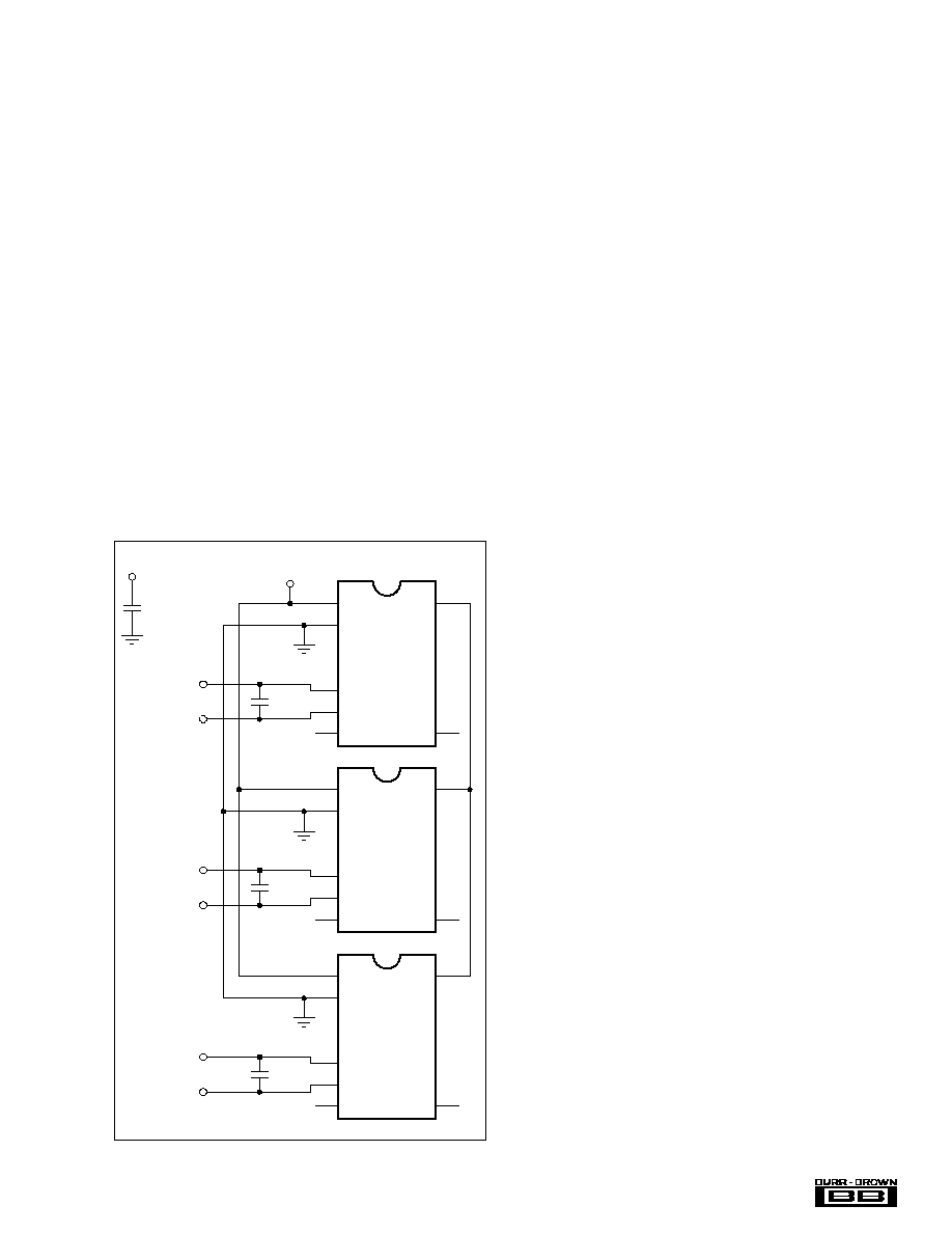
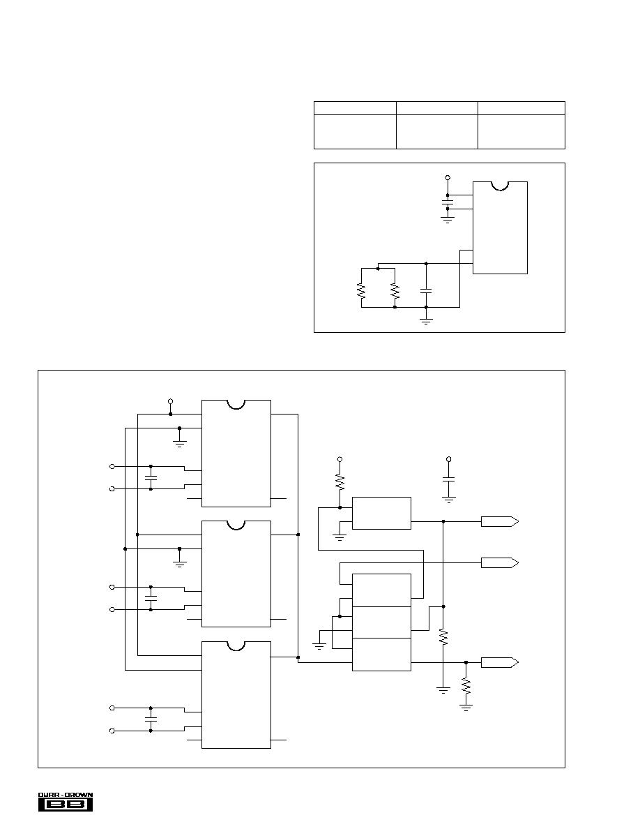
1 per DCP01
ÙOut 1
+Out 1
ÙOut 2
+Out 2
ÙOut 3
+Out 3
FIGURE 1. Standard Interface.
Û
DCP0105
14
performance decrease. Driving the SYNC
IN
pin with a CPU
type tri-state output, which has a low output capacitance,
offers the lowest reduction in performance.
DECOUPLING
Ripple Reduction
The high switching frequency of 400kHz allows simple
filtering. To reduce ripple, it is recommended that 0.47
ç
F
capacitors are used on V
S
and V
OUT
(see Figure 2). Both
outputs on dual output DCP0105 devices should be decoupled
to pin 5. In applications where power is supplied over long
lines and output loading is high, it may be necessary to use
a 2.2
ç
F capacitor on the input to insure startup.
There is no restriction on the size of the output capacitor
used to reduce ripple. The DCP0105 will start into any
capacitive load. Low ESR capacitors will give the best
reduction.
EXTERNAL SYNCHRONIZATION
The DCP0105 can be synchronized externally if required
using a simple external interface. Figure 3 shows a universal
interface using a 4066 quad switch. The CTL and SYNC
ON
pins are used to select external synchronization or self-
synchronization.
This interface can also be used to stop (disable) the DCP0105.
CTL
SYNC
ON
FUNCTION
1
1
External Sync
--
0
Self-Sync
0
1
Device Stop
1
2
5
6
V
S
0V
0V
V
Out
C
1
0.47çF
C
2
0.47çF
R
2
330
+5V
R
1
27
2W
2W
DCP0105
FIGURE 2. DCP010505 Fully Loaded.
DCP0105
1
2
5
6
7
14
8
V
CC
0V
OutÙ
Out+
SYNC
I/O
1A
I/O
1B
U1
CONT
C
2
470nF
C
3
470nF
C
1
470nF
(One Per
DC/DC)
DCP0105
1
2
5
6
7
14
8
V
CC
0V
OutÙ
Out+
SYNC
R
1
33k
R
2
33k
DCP0105
1
2
5
6
7
14
8
V
CC
0V
OutÙ
Out+
SYNC
C
4
470nF
+5V
+5V
+5V
ÙOut 1
+Out 1
ÙOut 2
+Out 2
ÙOut 3
+Out 3
I/O
1A
I/O
1B
U3
CONT
I/O
1A
I/O
1B
U4
CONT
I/O
1A
I/O
1B
U5
CONT
SYNC ON
FREQ IN
CTL
R
3
33k
0V
0V
0V
0V
0V
4066
FIGURE 3. Universal Interface.
15
Û
DCP0105
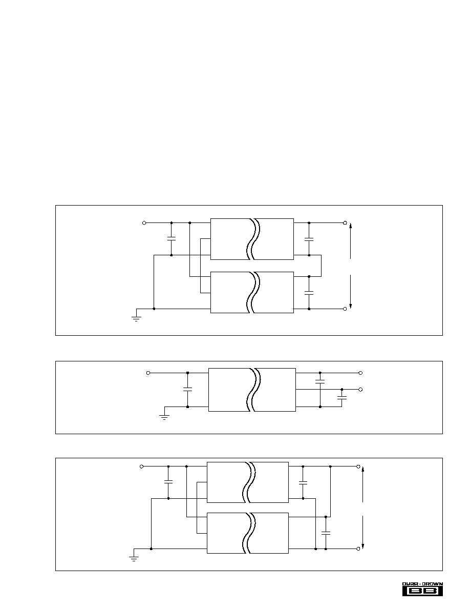
Connecting the DCP0105 in Parallel
If the output power from one DCP0105 is not sufficient, it
is possible to parallel the outputs of multiple DCP0105s (see
Figure 6). Again, the SYNC feature allows easy synchroni-
zation to prevent power-rail beat frequencies at no additional
filtering cost.
THERMAL MANAGEMENT LAYOUT
To maximize the thermal performance of the DCP0105,
taking more care in the PCB layout can provide the most
efficient thermal dissipation paths from the DC/DC. The
input controller IC and the rectifier diodes inside the DCP0105
are bonded directly onto the internal leadframe. The
leadframe, being almost 100% copper, provides an excellent
path for dissipated heat and does so significantly more
efficiently than FR4 PCBs or ceramic substrates found in
alternate packaging technology DC/DCs.
Connecting the DCP0105 in Series
Multiple DCP0105 isolated 1W DC/DC converters can be
connected in series to provide non-standard voltage rails.
This is possible by utilizing the floating outputs provided by
the DCP0105's galvanic isolation.
Connect the positive V
OUT
from one DCP0105 to the nega-
tive V
OUT
(0V) of another (see Figure 4). If the SYNC
IN
pins
are tied together, the self-synchronization feature of the
DCP0105 will prevent beat frequencies on the voltage rails.
The SYNC feature of the DCP0105 allows easy series
connection without external filtering which is necessary in
competing solutions.
The outputs on dual output DCP0105 versions can also be
connected in series to provide 2 times the magnitude of
V
OUT
(see Figure 5). For example, a dual 12V DCP010512D
could be connected to provide a 24V rail.
DCP
0105
0V
0V
V
OUT
V
SUPPLY
V
S
0V
DCP
0105
V
OUT
2 x Power Out
SYNC
IN
SYNC
IN
V
S
0V
COM
FIGURE 6. Connecting Multiple DCP0105s in Parallel.
FIGURE 5. Connecting Dual Outputs in Series.
DCP
0105
+V
OUT
V
SUPPLY
+V
OUT
ÙV
OUT
ÙV
OUT
0V
V
S
0V
COM
FIGURE 4. Connecting the DCP0105 in Series.
DCP
0105
V
OUT 1
V
SUPPLY
V
S
0V
DCP
0105
V
OUT 2
V
OUT1
+ V
OUT 2
SYNC
IN
SYNC
IN
V
S
0V
0V
0V
COM

Û
DCP0105
16
Most of the dissipated heat comes from input side common
(pin 2). To a lesser extent, the +V
OUT
pin (pin 6) also
dissipates heat from the package. In the layout shown in
Figure 7, the large copper areas next to pins 2 and 6 will
provide excellent heat dissipation paths.
The tracking in Figure 7, shown in dotted lines, will provide
shielding for the SYNC
IN
(pin 14) and SYNC
OUT
(pin 7)
pins if necessary.
As described earlier in the Disable/Enable section of this
data sheet, any additional capacitance to the 25pF internal
capacitor at the SYNC
IN
pin will affect performance. If there
is the possibility of significant leakage capacitance at the
SYNC
IN
pin, it can be shielded as shown.
As described earlier in the Synchronization section of this
data sheet, the SYNC
OUT
pin can be shielded as shown to
minimize noise pick-up in sensitive applications.
FIGURE 8. PCB Layout for DCP0105 and Competitive SIP
DC/DC.
DCP01xx
SIP DC/DC
+V
IN
ÙV
IN
0V
+V
OUT
ÙV
OUT
FIGURE 9. DCP010505P AND LP2986 Regulator.
FIGURE 7. Thermal Management Layout.
Bottom View
I
OUT
(mA)
V
REG
(V)
5.0
4.8
4.6
4.4
4.2
4.0
3.8
0
50
100
150
200
V
IN
= 5V
V
IN
= 5.25V
V
IN
= 4.75V
LAYOUT FOR DCP0105 AND SIP PRODUCTS
Figure 8 shows a layout to allow the use of a DCP0105 and
a competitive SIP isolated DC/DC converter.
POST REGULATION OF THE DCP010505P USING
THE LP2986 LDO REGULATOR
In digital applications where the load range is wide or
evolving, or the input supply voltage is not well regulated
and 5V
Ý
5% or 5V
Ý
V10% cannot be guaranteed, it is often
necessary to have a regulated 5V output from the DCP0105.
It is possible to post regulate the 5V
OUT
DCP0105 and still
guarantee a minimum V
OUT
of 4.75V. This still gives the
benefits of isolation in reducing the power supply noise to
5V digital circuitry.
By using an ultra-low dropout regulator (e.g., National
Semiconductor's LP2986IM-5.0) in series with the output of
a 5V
OUT
DCP0105, it is possible to supply up to 100% load
current (depending on V
IN
). Figure 9 shows the typical load
current for the post-regulated 5V
IN
/5V
OUT
DCP010505. It is
possible with a V
IN
of 5V to supply 130mA. Because of the
1:1 line regulation of the DCP0105, a 5% change in the input
will result in a 5% change in the output. Therefore, the
amount of current that the LDO can deliver is strongly
dependent on the V
IN
of the DCP010505. With a V
IN
of
5.25V, the LP2986 LDO can deliver up to 165mA.
The LP2986 LDO has a very low dropout voltage of typi-
cally less than 180mV, which allows us to deliver 4.75V
guaranteed from a 5V
OUT
unregulated DC/DC. It also offers
low output flagging and shutdown capability and is supplied
in either MSOP-8 or SO-8 packages ensuring additional
board area is minimal and low profile is maintained.
DCP01 AND LP2986 APPLICATION CIRCUIT
Figure 10 shows the LP2986 in series with the DCP010505
output. The 2.2
ç
F capacitor on the input of the LP2986 and
the 4.7
ç
F capacitor on the output are the minimum recom-
mended for good ripple reduction. Pin 7 on the LP2986 flags
an error by going LOW if the output drops 5% below
nominal.

17
Û
DCP0105
OTHER LDO REGULATORS
The SGS-Thomson L4940V5 LDO can also be used to post
regulate the 5V
OUT
DCP010505 and can deliver a regulated
minimum 4.75V up to 135mA.
The 5V
OUT
DCP010505 can also be post regulated with the
Micrel MIC5207 which offers up to 180mA output drive
with a typical dropout voltage of 165mV at 150mA. The
MIC5207 is available in a micro-sized SOT23-5 package
which gives the minimum additional board area for post
regulation.
PREDICTING OUTPUT VOLTAGE VERSUS LOAD
The Load Regulation specifications are calculated as fol-
lows:
DCP
0105
5
6
4
3
2
1
5
6
7
8
1
2
0.47çF
2.2çF
4.7çF
Load
+
330k
Error
Output
Com
LP2986
V
IN
0V
FIGURE 10. Post Regulation of DCP010505P.
15.24 (0.600)
11.8 (0.464)
14-Pin
All Leads on 2.54mm Pitch
Dimensions in mm (inches)
1.9 (0.075)
2.54 (0.100)
1.2 (0.047)
FIGURE 11. PCB Pad Size and Placement for "U" Package.
CONDITION
CALCULATION
10% to 100% Load
(V
OUT
at 10% load Ù V
OUT
at 100% load)/ V
OUT
at 75% load
10% to 25% Load
(V
OUT
at 10% load Ù V
OUT
at 25% load)/ V
OUT
at 25% load
10% to 75% Load
(V
OUT
at 10% load Ù V
OUT
at 75% load)/ V
OUT
at 75% load
75% to 100% Load
(V
OUT
at 75% load Ù V
OUT
at 100% load)/ V
OUT
at 75% load
2. To predict the output voltage at 10% load take the mea-
sured or specified voltage at 75% load and multiply by
(1 + Load Reg 10% to 75%). For example a DCP010505P
typical V
OUT
at 10% load will be 5V
x
(1 + 17%) = 5.85V.
3. To predict the output voltage at 25% load on higher V
OUT
versions take the measured or specified voltage at 75%
load and multiply by (1 + Load Reg 25% to 75%). For
example a DCP010512P typical V
OUT
at 25% load will be
12V
x
(1 + 12%) = 13.4V. To then estimate the voltage at
10% load take the previously calculated V
OUT
at
25% load and multiply by (1 + Load Reg 10% to 25%).
In this case the typical V
OUT
at 10% load will be 13.4V
x
(1 + 7%) = 14.3V.
To obtain predictions for loads other than those specified
assume the V
OUT
versus load characteristic is linear between
the load points and calculate accordingly. The 10% to 100%
load specification guarantees the maximum voltage excursion
for any load between 10% to 100% with respect to V
OUT
at
75% load.
The above does not take into consideration line regulation and
assumes a nominal input voltage. The 1:1 line regulation of the
DCP01 family means that a percentage change in the input
will give a corresponding percentage change in the output.
1. To predict the output voltage at 100% load take the mea-
sured or specified voltage at 75% load and multiply by
(1 + Load Reg 75% to 100%). For example a DCP010505P
typical V
OUT
at 100% load will be 5V
x
(1 Ù 8%) = 4.6V.