Altima Communications Inc.
AC104QF
Ultra Low Power 10/100 Quad RMII Ethernet Transceiver
GENERAL DESCRIPTION
The AC104QF is a highly integrated, 3.3V, low
power, four port, 10Base-T/100Base-TX/FX,
Ethernet transceiver implemented in 0.35
µ
m CMOS
technology. Multiple modes of operation including
normal operation, test mode and power saving mode
are available through either hardware or software
control.
Features include MAC interfaces, ENDECs,
Scrambler/Descrambler, and Auto-Negotiation
(ANeg) with support for parallel detection. The
transmitter includes a dual-speed clock synthesizer
that only needs one external clock source. The chip
has built-in wave shaping driver circuit for both
10Mbps and 100Mbps, eliminating the need for an
external hybrid filter. The receiver has an adaptive
equalizer / DC restoration circuit for accurate clock /
data recovery for the 100Base-TX signal. It also
provides an on-chip low pass filer / Squelch circuit
for the 10Base-T signal.
MAC interfaces support four ports of 10/100 RMII.
Media Interfaces support 4 ports of 10/100TX or 3
ports 10/100TX and 1 port 100FX.
FEATURES
·
4 RMII
·
RMII 5Volt tolerant and 2.5Volt capable
·
4 10/100 TX or 3 10/100 TX and 1 100 FX
·
Full Duplex or Half Duplex
·
FEFI on 100FX
·
Very small package
·
100PQFP
·
Very low power TYP < 280mW (/ port)
·
Cable Detect mode TYP < 40mW (/ port)
·
Power Down mo de TYP < 3.3mW (/ port)
·
Selectable TX drivers for 1:1 or 1.25:1
transformers for additional power reduction
·
3.3Volt .35micron CMOS
·
Fully compliant with
·
IEEE 802.3 / 802.3u
·
RMII
·
UNH test labs
·
Baseline Wander Compensation
·
Multi-Function LED outputs
·
Cable length indicator
·
Reverse polarity detection and correction with
Register Bit indication Automatic or Forced
·
8 programmable interrupts
·
Diagnostic registers
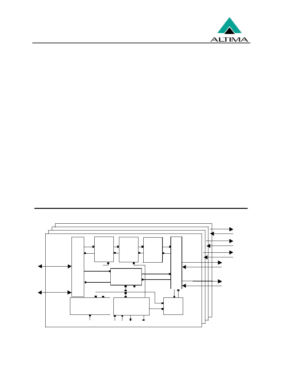
BLOCK DIAGRAM
PCS
.Framer
.Carrier Detect
.4B/5B
CKIN
TEST[3:0]
RMII/MII
MII SMI
10BASE-T
MII Serial Management
Interface and Registers
Auto-
Negotiation
100TX
100RX
10TX
10RX
FLP
RX
Control/Status
20
MHz
25
MHz
25
MHz
PLL
Clk Gen.
Test/LED Control
PHYAD[4:0]
XTLP/N
LED Drivers
Interface
Mux
TP_PMD
.MLT-3
.BLW
.Stream Cipher
PMA
.Clock
Recov.
.Link Monitor
.Signal Detect
TXOP/N(1)
RXIP/N(1)
TXOP/N(0)
RXIP/N(0)
TXOP/N(2)
RXIP/N(2)
TXOP/N(3)
RXIP/N(3)
FXTP/N(3)
FXRP/N(3)
Port 3
Port 2
Port 1
Port 0

AC104QF
Ultra Low Power 10/100 Quad RMII Ethernet Transceiver
2055 Gateway Parkway Suite 700, San Jose, CA 95110 (408) 453-3700 (www.altimacom.com)
Altima Communications Inc. reserves the right to make changes to this document without notice.
Document Revision 4.0
Page 2 of 37
REVISION HISTORY
REVISION#
DATE
CHANGE BY
CHANGE DESCRIPTION
1.0
July 1998
xx
Preliminary Release
3.2
June 2000
xx
Final Release
4.0
Sept 12, 2000
Helene
1. Change the default value of register 3 [15:0] =
101010101000001 on page 20
2. Enhance the descriptions of the DPLX and SPEED (register
18.11 and 18.10) on page 24

AC104QF
Ultra Low Power 10/100 Quad RMII Ethernet Transceiver
2055 Gateway Parkway Suite 700, San Jose, CA 95110 (408) 453-3700 (www.altimacom.com)
Altima Communications Inc. reserves the right to make changes to this document without notice.
Document Revision 4.0
Page 3 of 37
General Description......................................................................................................................................................................... 1
Features.............................................................................................................................................................................................. 1
Block Diagram................................................................................................................................................................................. 1
Pin Diagram - AC104QF................................................................................................................................................................ 5
Pin Descriptions............................................................................................................................................................................... 6
MDI (Media Dependent Interface) Pins.....................................................................................................................................6
RMII (Reduced Media Independent Interface) Pins................................................................................................................7
SMI (Serial Management Interface) Pins ..................................................................................................................................7
Phy Address Pins...........................................................................................................................................................................8
Mode Pins........................................................................................................................................................................................8
LED Pins .........................................................................................................................................................................................8
Power and Ground Pins ................................................................................................................................................................9
Functional Description.................................................................................................................................................................. 10
MAC Interface................................................................................................................................................................................ 10
RMII ...................................................................................................................................................................................................10
SMI
...............................................................................................................................................................................................10
Interrupt.........................................................................................................................................................................................11
Carrier Sense / RX_DV ..............................................................................................................................................................11
Media Interface .............................................................................................................................................................................. 11
10Base-T ...........................................................................................................................................................................................11
Transmit Function........................................................................................................................................................................11
Receive Function .........................................................................................................................................................................11
Link Monitor.................................................................................................................................................................................11
100Base-TX ......................................................................................................................................................................................11
Transmit Function........................................................................................................................................................................11
Parallel to Serial, NRZ to NRZI, and MLT3 Conversion....................................................................................................12
Receive Function .........................................................................................................................................................................12
Baseline Wander Compensation...............................................................................................................................................12
Clock/Data Recovery ..................................................................................................................................................................12
Decoder/De-scrambler ................................................................................................................................................................13
Link Monitor.................................................................................................................................................................................13
100Base-FX......................................................................................................................................................................................13
Transmit Function........................................................................................................................................................................13
Receive Function .........................................................................................................................................................................13
Link Monitor.................................................................................................................................................................................13
Far-End-Fault-Indication (FEFI)...............................................................................................................................................13
10Base-T/100Base-TF/FX .............................................................................................................................................................14
Multi-Mode Transmit Driver.....................................................................................................................................................14
Adaptive Equalizer ......................................................................................................................................................................14
PLL Clock Synthesizer ...............................................................................................................................................................14
Jabber and SQE (Heartbeat).......................................................................................................................................................14
Reverse Polarity Detection and Correction .............................................................................................................................14
Initialization and Setup................................................................................................................................................................. 15
Hardware Configuration................................................................................................................................................................15
Software Configuration ..................................................................................................................................................................15
LEDs ..............................................................................................................................................................................................15
Auto-Negotiation.............................................................................................................................................................................15
Parallel Detection...........................................................................................................................................................................16
Diagnostics.......................................................................................................................................................................................16
Loopback Operation....................................................................................................................................................................16
Cable Length Indicator...............................................................................................................................................................16
Reset and Power............................................................................................................................................................................. 16
Clock................................................................................................................................................................................................ 17
Register Descriptions.................................................................................................................................................................... 18

AC104QF
Ultra Low Power 10/100 Quad RMII Ethernet Transceiver
2055 Gateway Parkway Suite 700, San Jose, CA 95110 (408) 453-3700 (www.altimacom.com)
Altima Communications Inc. reserves the right to make changes to this document without notice.
Document Revision 3.2
Page 4 of 37
Registers 1-7.....................................................................................................................................................................................18
Registers 8-31...................................................................................................................................................................................18
Register 0: Control Register.......................................................................................................................................................19
Register 1: Status Register.........................................................................................................................................................20
Register 2: PHY Identifier 1 Register......................................................................................................................................20
Register 3: PHY Identifier 2 Register......................................................................................................................................20
Register 4: Auto-Negotiation Advertisement Register..........................................................................................................21
Register 5: Auto-Negotiation Link Partner Ability Register/Link Partner Next Page Message....................................21
Register 6: Auto-Negotiation Expansion Register.................................................................................................................22
Register 7: Auto-Negotiation Next Page Transmit Register................................................................................................22
Register 16: BT and Interrupt Level Control Register..........................................................................................................23
Register 17: Interrupt Control/Status Register........................................................................................................................23
Register 18: Diagnostic Register...............................................................................................................................................24
Register 19: Power/Loopback Register....................................................................................................................................24
Register 20: Cable measurement capability Register............................................................................................................24
Register 21: Receive Error Counter..........................................................................................................................................24
Register 24: Mode Control Register.........................................................................................................................................25
Mode Table ...................................................................................................................................................................................25
4B/5B Code-Group Table ............................................................................................................................................................ 26
SMI Read/Write Sequence........................................................................................................................................................... 27
LED Configurations...................................................................................................................................................................... 27
ELECTRICAL CHARACTERISTICS ...................................................................................................................................... 27
ELECTRICAL CHARACTERISTICS ...................................................................................................................................... 28
Absolute Maximum Ratings...........................................................................................................................................................28
Operating Range..............................................................................................................................................................................28
Total Power Consumption..........................................................................................................................................................28
TTL I/O Characteristics ..............................................................................................................................................................28
REFCLK and XTAL Pins ..........................................................................................................................................................28
I/O Characteristics LED/CFG Pins .......................................................................................................................................29
100 BASE-TX Transceiver Characteristics ............................................................................................................................29
10 BASE-T Transceiver Characteristics..................................................................................................................................29
100 BASE-FX Transceiver Characteristics.............................................................................................................................30
10 BASE-T Link Integrity Timing Characteristics................................................................................................................30
Digital Timing Characteristics .....................................................................................................................................................31
Power on Reset.............................................................................................................................................................................31
Management Data Interface .......................................................................................................................................................31
100Base-TX/FX & 10Base-T RMII Transmit System Timing ...........................................................................................32
100Base-TX/FX & 10Base-T RMII Receive System Timing .............................................................................................33
TX Application Termination ..........................................................................................................................................................34
FX Application Termination..........................................................................................................................................................35
Power and ground filtering for AC104QF..................................................................................................................................36
Package dimensions for AC104QF (100 pin PQFP) ................................................................................................................37

AC104QF
Ultra Low Power 10/100 Quad RMII Ethernet Transceiver
2055 Gateway Parkway Suite 700, San Jose, CA 95110 (408) 453-3700 (www.altimacom.com)
Altima Communications Inc. reserves the right to make changes to this document without notice.
Document Revision 3.2
Page 5 of 37
RX
IN(0)
RXIP(0) AGND
AGND
TXOP(0)
TXON(0)
AVDD
AVDD
TXON(1) TXOP(1)
AGND AGND
RXIP(1) RXIN(1)
AVCC
AVCC
RXIN(2) RXIP(2)
AGND
AGND
TXOP(2)
TXON(2)
AVDD
AVDD
TXON(3)
TXOP(3)
AGND
AGN
RXIP(3)
RXIN(3)
OVDD
RXD[0](0)
RXD[1](0)
CVDD
TX_EN(1)
TXD[0](1)
TXD[1](1)
OGND
OGND
CRS_DV(1)
R
X_ER(1)
RXD[0](1)
RXD[1](1)
CVDD
REF_CLK
MDC
MDIO
TX_EX(2)
OVDD
TXD[0](2)
TXD[1](2)
CGND
CRS_DV(2)
RX)ER(2)
RXD[0](2)
RXD[1](2)
CVDD
TX_EX(3)
OGND
TXD[0](3)
PIN DIAGRAM - AC104QF
RX_ER(0)
81
50
TXD[1](3)
CRS_DV(0)
82
49
CGND
CGND
83
48
CRS_DV(3)
TXD[1](0)
84
47
RX_ER(3) / PHYAD_ST
TXD[0](0)
85
46
RXD[0](3)
TX_EN(0)
86
45
RXD[1](3)
OGND
87
44
OVDD
LEDDPX(1) / PHYAD[4]
88
43
LEDSPD(2) / FORCE100
LEDACT(1) / PHYAD[3]
89
42
LEDACT(2)
LEDSPD(1) / PHYAD[2]
90
41
LEDDPX(2)
LEDDPX(0) / FX_DIS
91
40
LEDSPD(3) / BURN_IN*
LEDACT(0)
92
39
LEDACT(3) / ANEGA
LEDSPD(0) / TP125
93
38
LEDDPX(3) / SCRAM_EN
INTR
94
37
FXTN(3)
RST*
95
36
FXTP(3)
GAGND
96
35
FXRN(3) / TST[3]
IBREF
97
34
FXRP(3) / TST[2]
GAVDD
98
33
SDN(3) / TST[1]
GAVDD
99
32
SDP(3) / TST[0]
AVDD
100
31
AVDD
1
2
3 4 5 6 7 8 9 10
11
12
13
14
15
16
17
18
19
20
21
22
23
24
25
26
27
28
29
30
80
79 78
77 76
75 74
73
72 71
70 69
68 67
66
65 64
63 62
61 60
59 58
57
56 55
54 53
52 51
AC104QF

AC104QF
Ultra Low Power 10/100 Quad RMII Ethernet Transceiver
2055 Gateway Parkway Suite 700, San Jose, CA 95110 (408) 453-3700 (www.altimacom.com)
Altima Communications Inc. reserves the right to make changes to this document without notice.
Document Revision 3.2
Page 6 of 37
PIN DESCRIPTIONS
Many of the pins of these devices have multiple functions. The multi-function pins will be designated by bolding of
the pin number. Separate descriptions of these pins will be listed in the proper sections. Designers must assure that
they have identified all modes of operation prior to final design.
NOTES:
The pin assignment shown below and in the pin description table is subject to change without notice. The user is
advised to contact Altima Communications Inc. before implementing any design based on the information provided in
this data sheet.
Signals types:
I = input
O = output
Z = high impedance
U = internally pull up
D = internally pull down
A = analog signal
* = Active Low Signal
NC = No Connect pin
MDI (Media Dependent Interface) Pins
Pin Name
Pin #
Type
Description
RXIN(0)
RXIN(1)
RXIN(2)
RXIN(3)
1
14
17
30
AI
AI
AI
AI
Receiver input Negative for both 10Base-T and 100Base-TX.
RXIP(0)
RXIP(1)
RXIP(2)
RXIP(3)
2
13
18
29
AI
AI
AI
AI
Receiver input Positive for both 10Base-T and 100Base-TX.
TXON(0)
TXON(1)
TXON(2)
TXON(3)
6
9
22
25
AO
AO
AO
AO
Transmitter output Negative for both 10Base-T and 100Base-TX.
TXOP(0)
TXOP(1)
TXOP(2)
TXOP(3)
5
10
21
26
AO
AO
AO
AO
Transmitter output Positive for both 10Base-T and 100Base-TX.
FXRP(3)
FXRN(3)
FXTP(3)
FXTN(3)
34
35
36
37
AI/O
AI/O
AO
AO
Receiver input Positive for 100Base-FX. (Port-3)
Receiver input Negative for 100Base-FX. (Port-3)
Transmitter output Positive for 100Base-FX. (Port-3)
Transmitter output Negative for 100Base-FX. (Port-3)
SDP(3)
SDN(3)
32
33
A/I,O
A/I,O
Signal Detect Input (For port 3 only). Indicates signal quality status on the fiber-
optic link in 100Base-FX mode. When the signal quality is good, the SDP pin
should be driven high relative to the SDN pin.

AC104QF
Ultra Low Power 10/100 Quad RMII Ethernet Transceiver
2055 Gateway Parkway Suite 700, San Jose, CA 95110 (408) 453-3700 (www.altimacom.com)
Altima Communications Inc. reserves the right to make changes to this document without notice.
Document Revision 3.2
Page 7 of 37
RMII (Reduced Media Independent Interface) Pins
Pin Name
Pin #
Type
Description
TXD[1:0](0)
TXD[1:0](1)
TXD[1:0](2)
TXD[1:0](3)
84, 85
74, 75
60, 61
50, 51
I/O, D
I/O, D
I/O, D
I/O, D
RMII Transmit Data. The MAC will source TXD[1:0](n) synchronous with
REFCLK when TX_EN(n) is asserted.
TX_EN(0)
TX_EN(1)
TX_EN(2)
TX_EN(3)
86
76
63
53
I/O,D
I/O,D
I/O,D
I/O,D
RMII Transmit Enable. TX_EN(n) is asserted high by the MAC to indicate that
valid data for transmission is presented on the TXD[1:0](n).
RXD[1:0](0)
RXD[1:0](1)
RXD[1:0](2)
RXD[1:0](3)
78,79
68,69
55,56
45,46
I/O, D
I/O, D
I/O, D
I/O, D
RMII Receive Data. The Phy will source RXD[1:0](n) synchronous with
REFCLK when CRS_DV(n) is asserted.
CRS_DV(0)
CRS_DV(1)
CRS_DV(2)
CRS_DV(3)
82
71
58
48
I/O, D
I/O, D
I/O, D
I/O, D
CRS_DV(n) is asserted high when media is non-idle.
RX_ER(0)
RX_ER(1)
RX_ER(2)
RX_ER(3)
81
70
57
47
I/O, D
O
O
I/O, D
RMII Receive Error. When RX_ER is asserted high, it indicates an error has
been detected during frame reception.
REFCLK
66
I
Reference Clock Input 50 MHz-100PPM TTL
SMI (Serial Management Interface) Pins
Pin Name
Pin #
Type
Description
MDIO
64
I/O, D
Management Data Input/Output. Bi-directional data interface. 1.5K pull up
resistor required (as specified in IEEE-802.3).
MDC
65
I, D
Management Data Clock. 0 to 25 MHz clock sourced by the MAC for transfer of
MDIO data.
INTR
94
Z
Interrupt. See Registers 16 and 17 for polarity and sources. The INTR pin has a
high impedance output, a 1K
pull-up or pull-down resistor is needed.

AC104QF
Ultra Low Power 10/100 Quad RMII Ethernet Transceiver
2055 Gateway Parkway Suite 700, San Jose, CA 95110 (408) 453-3700 (www.altimacom.com)
Altima Communications Inc. reserves the right to make changes to this document without notice.
Document Revision 3.2
Page 8 of 37
Phy Address Pins
Pin Name
Pin #
Type
Description
PHYAD_ST
47
I/O,D
1 at reset = 0-XXX00, 1-XXX01, 2-XXX10, 3-XXX11
0 at reset = 0-XXX01, 1-XXX10, 2-XXX11, 3-XXX00
PHYAD [4]
PHYAD [3]
PHYAD [2]
88
89
90
I/O
I/O
I/O
PHY Address [4:2]. These pins set the three MSB's for SMI PHY address.
PHYAD [1:0] are internally wired to four ports. (See PHYAD_ST)
The PHYAD will also determine the scramble seed, this will help to reduce EMI
when there are multiple ports switching at the same time.
Mode Pins
Pin Name
Pin #
Type
Description
FX_DIS
91
I/O
FX Disable. Pulled low upon reset will put port 3 in 100FX mode.
TP125
93
I/O
Transformer Ratio. Pulled low upon reset will select transmit transformer ratio
to be 1.25:1. Pulled high is 1:1 transformer.
FORCE100
43
I/O
FORCE100: Force 100Base-X Operation. When this signal is pulled high and
ANENGA is low upon reset, all ports will be forced to 100Base-TX operation.
When asserted low and ANENGA is low, all ports are forced to 10Base-T
operation. When ANENGA is high, FORCE100 has no effect on operation.
SCRAM_EN
38
I/O
Scrambler Enable. Pulled low upon reset will bypass the scrambler. Pulled high
is scrambler enabled.
ANEGA
39
I/O
Auto-Negotiation Ability. Asserted high means auto-negotiation enable while
low means manual selection through FDXEN, F100.
BURN_IN*
40
I/O
Burn-In mode. Burn-in mode for reliability assurance control. This is reserved
for internal testing only.
LED Pins
Pin Name
Pin #
Type
Description
LEDDPX[0]
LEDDPX[1]
LEDDPX[2]
LEDDPX[3]
91
88
41
38
I/O,U
I/O,U
I/O,U
I/O,U
Port[n] Duplex LED. Active state indicates Full Duplex or Collision in Half
Duplex mode.
LEDACT_LNK[0]
LEDACT_LNK[1]
LEDACT_LNK[2]
LEDACT_LNK[3]
92
89
42
39
I/O,U
I/O,U
I/O,U
I/O,U
Port[n] Activity/Link LED. Active state indicates a valid link. When there is
receive or transmit activity, LED will toggle between high and low for 30 ms
interval.
LEDSPD[0]
LEDSPD[1]
LEDSPD[2]
LEDSPD[3]
93
90
43
40
I/O,U
I/O,U
I/O,U
I/O,U
Port[n] Speed LED. Active state indicates 100Base-TX mode.
Polarity of LEDs is determined by polarity of mode pins. See LED example

AC104QF
Ultra Low Power 10/100 Quad RMII Ethernet Transceiver
2055 Gateway Parkway Suite 700, San Jose, CA 95110 (408) 453-3700 (www.altimacom.com)
Altima Communications Inc. reserves the right to make changes to this document without notice.
Document Revision 3.2
Page 9 of 37
Miscellaneous Pins
Pin Name
Pin #
Type
Description
RST*
95
I, U
Reset. An active low input will force a known initialization state. The reset pulse
duration must be > 100 us. Setting MII Reg. 0.15 will assert software reset,
which has the same functionality as the hardware reset.
IBREF
97
A
Reference Bias Resistor. Must be tied to analog ground through an external
10K
(1%) resistor.
TST[0]
TST[1]
TST[2]
TST[3]
32
33
34
35
A/I,O
Test. Outputs during test mode.
Power and Ground Pins
Pin Name
Pin #
Type
Description
OVDD
44, 62, 80
P
Digital +3.3V power supply for I/O.
OGND
52, 72, 87
G
Digital ground for I/O.
CVDD
54, 67, 77
P
Digital +3.3V power supply for Core logic.
CGND
49, 59, 73,
83
G
Digital ground for Core logic.
AVDD
7, 8, 15,
16, 23, 24,
31, 100
P
+3.3V power supply for Analog circuit.
AGND
3, 4, 11,
12, 19, 20,
27, 28
G
Ground for Analog circuit.
GAVDD
98,99
P
+3.3V power supply for common analog circuits.
GAGND
96
G
Ground for common analog circuits.

AC104QF
Ultra Low Power 10/100 Quad RMII Ethernet Transceiver
2055 Gateway Parkway Suite 700, San Jose, CA 95110 (408) 453-3700 (www.altimacom.com)
Altima Communications Inc. reserves the right to make changes to this document without notice.
Document Revision 3.2
Page 10 of 37
FUNCTIONAL DESCRIPTION
The AC104QF physical layer device (Phy) integrates
the 100Base-X and 10Base-T functions in a single
four port chip that is used in Fast Ethernet 10/100
Mbps applications. The 100Base-X section consists
of PCS, PMA, and PMD functions, and the 10Base-T
section consists of Manchester ENDEC and
transceiver functions. The device performs the
following functions:
·
4B/5B
·
MLT3
·
NRZI
·
Manchester Encoding and Decoding
·
Clock and Data Recovery
·
Stream Cipher Scrambling / De-Scramb ling
·
Adaptive Equalization
·
Line Transmission
·
Carrier Sense
·
Link Integrity Monitor
·
Auto-Negotiation (ANeg)
·
RMII MAC connectivity
·
MII Management Function
It also provides an RMII consortium compatible
Reduced Media Independent Interface (RMII) to
communicate with an Ethernet Media Access
Controller (MAC). Selection of 10 or 100 Mbps
operation is based on the settings of internal Serial
Management Interface registers or determined by the
on-chip ANeg logic. The device can operate in 10 or
100 Mbps with full duplex or half-duplex mode on a
per port basis. Port 3 can also be configured for
100Base-FX.
MAC INTERFACE
RMII
The Reduced Media Independent Interface (RMII) is
used to connect the Phy with the MAC. The PHY
and MAC obtain their clock from a common 50 MHz
source, such as a clock oscillator. This clock is
shared by all ports within the Phy for transmitting
and receiving data on 2 individual 2-bit data buses.
CRS and RXDV are muxed together to indicate to the
MAC when there is valid data on the receive bus. In
100M mode RXD[1:0] is sampled on every cycle of
REFCLK. In 10M mode RXD[1:0] is sampled on
every 10
th
cycle of REFCLK. RXER is generated by
the Phy to indicate a receive error to the MAC.
TX_EN is generated by the MAC to indicate to the
Phy when there is valid data on the transmit bus. In
100M mode the Phy will read 2 bits from TXD[1:0]
for each cycle of REFCLK. In 10M mode the Phy
will read 2 bits of data from TXD[1:0] every 10
th
cycle of REFCLK.
The Serial Management Interface (SMI) is shared
between all ports in the Phy. This totals 7 pins per
port plus 3 per Phy, whereas MII has 18 pins per port.
SMI
The Phy's internal registers are accessible only
through the MII 2-wire Serial Management Interface
(SMI). MDC is a clock input to the Phy which is
used to latch in or out data and instructions for the
Phy. The clock can run at any speed from DC to 25
MHz. MDIO is a bi-directional connection used to
write instructions to, write data to, or read data from
the Phy. Each data bit is latched either in or out on
the rising edge of MDC. MDC is not required to
maintain any speed or duty cycle, provided no half
cycle is less than 20ns and that data is presented
synchronous to MDC.
MDC/MDIO are a common signal pair to all ports on
a design. Therefore, each port needs to have its own
unique Physical Address. The Physical Address of
the Phy is set using the pins defined as PHYAD[4:2].
These input signals are strapped externally and
sampled as reset is negated. PHYAD[1:0] are
addressed for each port internal to the Phy. Internal
addresses are either 00, 01, 10, 11 or 01, 10, 11, 00
depending on the polarity of PHYAD_ST during
reset.
At idle, the PHY is responsible to pull MDIO line to
a high state. Therefore, a 1.5K Ohms resistor is
required to connect MDIO line to Vcc. The PHYAD
can be reprogrammed via software. A detailed
definition of the Serial Management registers
follows.
At the beginning of a read or write cycle, the MAC
will send a continuous 32 bits of one at the MDC
clock rate to indicate preamble. A zero and a one
will follow to indicate start of frame. A read OP
code is a one and a zero, while a write OP code is a
zero and a one. These will be followed by 5 bits to
indicate PHY address and 5 bits to indicate register
address. Then 2 bits follow to allow for turn around
time. For read operation, the first bit will be high
impedance. Neither the PHY nor the station will
assert this bit. During the second bit time, the PHY

AC104QF
Ultra Low Power 10/100 Quad RMII Ethernet Transceiver
2055 Gateway Parkway Suite 700, San Jose, CA 95110 (408) 453-3700 (www.altimacom.com)
Altima Communications Inc. reserves the right to make changes to this document without notice.
Document Revision 4.0
Page 11 of 37
will assert this bit to a zero. For write operation, the
station will drive a one for the first bit time, and a
zero for the second bit time. The 16 bits data field is
then presented. The first bit that is transmitted is bit
15 of the register content. (See SMI Read/Write
Sequence)
Interrupt
The INTR pin on the Phy will be asserted whenever
one of 8 selectable interrupt events occur. Assertion
state is programmable to either high or low through
the INTR_LEVL register bit. Selection is made by
setting the appropriate bit in the upper half of the
Interrupt Control / Status register. When the INTR
bit goes active, the MAC interface is required to read
the Interrupt Control / Status register to determine
which event caused the interrupt. The Status bits are
read only and clear on read. When INTR is not
asserted, the pin is held in a high impedance state.
Carrier Sense / RX_DV
Carrier sense is asserted asynchronously on the CRS
pins as soon as activity is detected on the receive data
stream. RX_DV is asserted as soon as a valid SSD
(Start-of-Stream Delimiter) is detected. Carrier sense
and RX_DV are de-asserted synchronously upon
detection of a valid end of stream delimiter or two
consecutive idle code groups in the receive data
stream. However, if the carrier sense is asserted and a
valid SSD is not detected immediately, RX_ER is
asserted instead of RX_DV.
In 10Base-T mode, CRS is asserted asynchronously
when the valid preamble and data activity is detected
on the RXIP and RXIN pins.
In the half duplex mode, the CRS is activated during
the transmit and receiving of data. In the full duplex
mode, the CRS is activated during data reception
only.
MEDIA INTERFACE
10BASE-T
When configured to run in 10Base-T mode, either
through hardware configuration, software
configuration or ANeg, the Phy will support all the
features and parameters of the industry standards.
Transmit Function
Parallel to Serial logic is used to convert the 2-bit
(RMII) or 4-bit (MII) data into the serial stream. The
serialized data goes directly to the Manchester
encoder where it is synthesized through the output
waveshaping driver. The waveshaper reduces any
EMI emission by filtering out the harmonics,
therefore eliminating the need for an external filter.
Receive Function
The received signal passes through a low-pass filter,
which filters out the noise from the cable, board, and
transformer. This eliminates the need for a 10Base-T
external filter. A Manchester decoder converts the
incoming serial stream. Serial to Parallel logic is
used to generate the 2-bit (RMII) or 4-bit (MII) data.
Link Monitor
The 10-Base-T link-pulse detection circuit will
constantly monitor the RXIP/RXIN pins for the
presence of valid link pulses. In the absence of valid
link pules, the Link Status bit will be cleared and the
Link LED will de-assert.
100BASE-TX
When configured to run in 100Base-TX mode, either
through hardware configuration, software
configuration or ANeg, the Phy will support all the
features and parameters of the industry standards.
Transmit Function
In 100Base-TX mode, the Phy transmit function
converts synchronous 2-bit (RMII) or 4-bit (MII) data
to a pair of 125 Mbps differential serial data streams.
The serial data is transmitted over network twisted
pair cables via an isolation transformer. Data
conversion includes 4B/5B encoding, scrambling,
parallel to serial, NRZ to NRZI, and MLT-3
encoding. The entire operation is synchronous to 25
MHz and 125 MHz clock. Both clocks are generated
by an on-chip PLL clock synthesizer that is locked on
to an external 25 MHz clock source.
The transmit data is transmitted from the MAC to the
Phy via the TXD[n:0] signals. The 4B/5B encoder
replaces the first two nibbles of the preamble from
the MAC frame with a /J/K/ code-group pair Start-of-
Stream Delimiter (SSD), following the onset of
TX_EN signal. The 4B/5B encoder appends a /T/R/
code-group pair End-of-Stream Delimiter (ESD) to
the end of transmission in place of the first two IDLE

AC104QF
Ultra Low Power 10/100 Quad RMII Ethernet Transceiver
2055 Gateway Parkway Suite 700, San Jose, CA 95110 (408) 453-3700 (www.altimacom.com)
Altima Communications Inc. reserves the right to make changes to this document without notice.
Document Revision 4.0
Page 12 of 37
code-groups that follow the negation of the TX_EN
signal. The encapsulated data stream is converted
from 4-bit nibbles to 5-bit code-groups. During the
inter-packet gap, when there is no data present, a
continuous stream of IDLE code-groups are
transmitted. When TX_ER is asserted while TX_EN
is active, the Transmit Error code-group /H/ is substi-
tuted for the translated 5B code word. The 4B/5B
encoding is bypassed when Reg. 21.1 is set to "1", or
the PCSBP pin is strapped high.
In 100Base-TX mode, the 5-bit transmit data stream
is scrambled as defined by the TP-PMD Stream
Cipher function in order to reduce radiated emissions
on the twis ted pair cable. The scrambler encodes a
plain text NRZ bit stream using a key stream periodic
sequence of 2047 bits generated by the recursive
linear function:
X[n] = X[n-11] + X[n-9] (modulo 2)
The scrambler reduces peak emissions by randomly
spreading the signal energy over the transmitted fre-
quency range, thus eliminating peaks at any single
frequency. For repeater applications, where all ports
transmit the same data simultaneously, signal energy
is spread further by using a non-repeating sequence
for each Phy, i.e., the scrambled seed is unique for
each different Phy based on the Phy address.
When Dis_Scrm is set to "0" the data scrambling
function is disabled, the 5-bit data stream is clocked
directly to the device's PMA sublayer.
Parallel to Serial, NRZ to NRZI, and MLT3
Conversion
The 5-bit NRZ data is clocked into Phy's shift
register with a 25 MHz clock, and clocked out with a
125 MHz clock to convert it into a serial bit stream.
The serial data is converted from NRZ to NRZI
format, which produces a transition on Logic 1 and
no transition on Logic 0. To further reduce EMI
emissions, the NRZI data is converted to an MLT-3
signal. The conversion offers a 3dB to 6dB reduction
in EMI emissions. This allows system designers to
meet the FCC Class B limit. Whenever there is a
transition occurring in NRZI data, there is a
corresponding transition occurring in the MLT-3
data. For NRZI data, it changes the count up/down
direction after every single transition. For MLT-3
data, it changes the count up/down direction after
every two transitions. The NRZI to MLT-3 data
conversion is implemented without reference to the
bit timing or clock information. The conversion
requires detecting the transitions of the incoming
NRZI data and setting the count up/down direction
for the MLT-3 data. Asserting FX_SEL high will
disable this encoding.
The slew rate of the transmitted MLT-3 signal can be
controlled to reduce EMI emissions. The MLT-3
signal after the magnetic has a typical rise/fall time of
approximately 4 ns, which is within the target range
specified in the ANSI TP- PMD standard. This is
guaranteed with either 1:1 or 1.25:1 transformer.
Receive Function
The 100Base-TX receive path functions as the
inverse of the transmit path. The receive path
includes a receiver with adaptive equalization and
DC restoration in the front end. It also includes a
MLT-3 to NRZI converter, 125 MHz data and clock
recovery, NRZI/NRZ conversion, Serial-to-Parallel
conversion, de-scrambler, and 5B/4B decoder. The
receiver circuit starts with a DC bias for the
differential RX+/- inputs, followed with a low-pass
filter to filter out high frequency noise from the
transmission channel media. An energy detect circuit
is also added to determine whether there is any signal
energy on the media. This is useful in the power-
saving mode. The amplification ratio and slicer's
threshold is set by the on-chip bandgap reference.
Baseline Wander Compensation
The 100Base-TX data stream is not always DC
balanced. The transformer blocks the DC components
of the incoming signal, thus the DC offset of the
differential receive inputs can drift. The shifting of
the signal level, coupled with non-zero rise and fall
times of the serial stream can cause pulse-width
distortion. This creates jitter and possible increase in
the bit error rates. Therefore, a DC restoration circuit
is needed to compensate for the attenuation of the DC
component. This Phy implements a patent-pending
DC restoration circuit. Unlike the traditional
implementation, the circuit does not need the
feedback information from the slicer or the clock
recovery circuit. This design simplifies the circuit
design and eliminates any random/systematic offset
on the receive path. In the 10BaseT and the 100Base-
FX modes, the baseline wander correction circuit is
not required, and therefore is disabled.
Clock/Data Recovery
The equalized MLT-3 signal passes through the slicer
circuit, and gets converted to NRZI format. The Phy
uses a proprietary mixed-signal phase locked loop
(PLL) to extract clock information from the incoming
NRZI data. The extracted clock is used to re-time the

AC104QF
Ultra Low Power 10/100 Quad RMII Ethernet Transceiver
2055 Gateway Parkway Suite 700, San Jose, CA 95110 (408) 453-3700 (www.altimacom.com)
Altima Communications Inc. reserves the right to make changes to this document without notice.
Document Revision 4.0
Page 13 of 37
data stream and set the data boundaries. The transmit
clock is locked to the 50 MHz clock input (RMII) or
25 MHz clock input (MII) while the receive clock is
locked to the incoming data streams. When initial
lock is achieved, the PLL switches to the data stream,
extracts the 125 MHz clock, and uses it for the bit
framing for the recovered data. The recovered 125
MHz clock is also used to generate the 25 MHz
MII_RXC (MII). The PLL requires no external
components for its operation and has high noise
immunity and low jitter. It provides fast phase
alignment and locks to data in one transition. Its
data/clock acquisition time after power-on is less than
60 transitions. The PLL can maintain lock on run-
lengths of up to 60 data bits in the absence of signal
transitions. When no valid data is present, i.e. when
the SD is de-asserted, the PLL will switch and lock
on to REFCLK. This provides a continuously running
MII_RXC (MII). At the PCS interface, the 5 bit data
RXD[4:0] is synchronized to the 25 MHz RX_CLK.
Decoder/De-scrambler
The de-scrambler detects the state of the transmit
Linear Feedback Shift Register (LFSR) by looking
for a sequence representing consecutive idle codes.
The de-scrambler acquires lock on the data stream by
recognizing IDLE bursts of 30 or more bits and locks
its frequency to its de-ciphering LFSR.
Once lock is acquired, the device can operate with an
inter-packet-gap (IPG) as low as 40 nS. However,
before lock is acquired, the de-scrambler needs a
minimum of 270 nS of consecutive idles in between
packets in order to acquire lock.
The de-ciphering logic also tracks the number of
consecutive errors received while the RX_DV is
asserted. Once the error counter exceeds its limit
currently set to 64 consecutive errors, the logic as-
sumes that the lock has been lost, and the de-cipher
circuit resets itself. The process of regaining lock
will start again.
Stream cipher de-scrambler is not used in the
100Base-FX and the 10Base-T modes.
Link Monitor
Signal level is detected through a squelch detection
circuitry. A signal detect (SD) circuit allows the
equalizer to assert high whenever the peak detector
detects a post-equalized signal with peak to ground
voltage greater than 400 mV. This is approximately
40% of a normal signal voltage level. In addition, the
energy level must be sustained for longer than 2~3
µ
S in order for the signal detect signal to stay on. The
SD gets de-asserted approximately 1~2
µ
s after the
energy level drops consistently below 300 mV from
peak to ground.
The link signal is forced low during a local loopback
operation (Loopback register bit is set) and forced to
high when a remote loopback is taking place
(EN_RPBK is set).
In forced 100Base-TX mode, when a cable is
unplugged or no valid signal is detected on the
receive pair, the link monitor enters in the "link fail"
state and NLP's are transmitted. When a valid signal
is detected for a minimum period of time, the link
monitor enters Link Pass State and transmits MLT-3
signal.
100BASE-FX
When port 3 is configured to run in 100Base-FX
mode, either through hardware configuration or
software configuration (100Base-FX does not support
ANeg) the Phy will support all the features and
parameters of the industry standards.
Transmit Function
The serialized data bypasses the scrambler and 4B/5B
encoder in FX mode. The output data is NRZI PECL
signals. The PECL level signals are used to drive the
Fiber-transmitter.
Receive Function
In 100Base-FX mode, signal is received through the
PECL receiver inputs, and directly passed to the
clock recovery circuit for data/clock extraction. In
FX mode, the scrambler/de-scrambler cipher function
is bypassed.
Link Monitor
In 100Base-FX mode, the external fiber-optic
receiver performs the signal energy detection
function and communicates this information directly
to the Phy's SDP pin.
Far-End-Fault-Indication (FEFI)
ANeg provides the mechanism to inform the link
partner that a remote fault has occurred. However,
ANeg is disabled in the 100Base-FX applications. An
alternative in-band signaling function (FEFI) is used
to signal a remote fault condition. FEFI is a stream of
84 consecutive ones followed by one logic zero. This

AC104QF
Ultra Low Power 10/100 Quad RMII Ethernet Transceiver
2055 Gateway Parkway Suite 700, San Jose, CA 95110 (408) 453-3700 (www.altimacom.com)
Altima Communications Inc. reserves the right to make changes to this document without notice.
Document Revision 4.0
Page 14 of 37
pattern is repeated 3 times. A FEFI will signal under
3 conditions: 1) When no activity is received from
the link partner, 2) When the clock recovery circuit
detects a signal error or PLL lock error, 3) When
management entity sets the transmit Far-End-Fault
bit.
The FEFI mechanism is enabled by default in the
100Base-FX mode, and is disabled in 100Base-TX or
10Base-T modes. The register setting can be changed
by software after reset.
10BASE-T/100BASE-TF/FX
Multi-Mode Transmit Driver
The multi-mode driver transmits the MLT-3 coded
signal in 100Base-TX mode, NRZI coded signal in
100Base-FX mode, and Manchester coded signal in
10Base-T mode.
In 100Base-FX mode, no filtering is performed. The
transmit driver utilizes a current drive output which is
well balanced and produces a low noise PECL signal.
PECL voltage levels are produced with resistive
terminations.
In 10BaseT mode, high frequency pre-emphasis is
performed to extend the cable-driving distance
without the external filter. The FLP and NLP pulses
are also drive out through the 10BaseT driver.
The 10BaseT and 100BaseTX transmit signals are
multiplexed to the transmit output driver. This
arrangement results in using the same external
transformer for both the 10BaseT and the
100BaseTX. The driver output level is set by a built-
in bandgap reference and an external resistor
connected to the IBREF pin. The resistor sets the
output current for all modes of operation. The
TXOP/N outputs are open drain devices with a serial
source to I/O pad resistance of 10
max. When the
1:1 transformer is used, the current rating is 40 mA
for the 2Vp-p MLT-3 signal, and 100 mA for the
5Vp-p Manchester signal. One can use a 1.25:1
transmit transformer for a 20% output driver power
reduction. This will decrease the drive current to 32
mA for 100Base-TX operation, and 80 mA for
10Base-T operation.
Adaptive Equalizer
The Phy is designed to accommodate a maximum of
150 meters UTP CAT-5 cable. An AT&T 1061 CAT-
5 cable of this length typically has an attenuation of
31 dB at 100 MHz. A typical attenuation of 100-
meter cable is 21 dB. The worst case cable
attenuation is around 24-26 dB as defined by TP-
PMD specification.
The amplitude and phase distortion from the cable
cause inter-symbol interference (ISI) which makes
clock and data recovery difficult. The adaptive
equalizer is designed to closely match the inverse
transfer function of the twisted-pair cable. The
equalizer has the ability to changes its equalizer
frequency response according to the cable length.
The equalizer will tune itself automatically for any
cable, compensating for the amplitude and phase
distortion introduced by the cable.
PLL Clock Synthesizer
The Phy includes an on-chip PLL clock synthesizer
that generate 25 MHz and 125 MHz clocks for the
100Base-TX circuitry. It also generates 20 MHz and
100 MHz clocks for the 10BaseT and ANeg circuitry.
The PLL clock generator uses a fully differential
VCO cell that introduces very low jitter. The Zero
Dead Zone Phase Detection method implemented in
the Phy design provides excellent phase tracking. A
charge pump with charge sharing compensation is
also included to further reduce jitter at different loop
filter voltages. The on-chip loop filter eliminates the
need for external components and minimizes the
external noise sensitivity. Only one external 50 MHz
(RMII) or 25 MHz (MII) crystal or clock source is
required as a reference clock.
After power-on or reset, the PLL clock synthesizer
generates the 20 MHz clock output until the
100Base-X operation mode is selected.
Jabber and SQE (Heartbeat)
After the MAC transmitter exceeds the jabber timer
(46mS), the transmit and loopback functions will be
disabled and COL signal get asserted. After TX_EN
goes low for more than 500 ms, the TP transmitter
will reactivate and COL gets de-asserted. Setting
Jabber Disable will disable the jabber function.
When the SQE test is enabled, a COL pulse with 5-
15BT is asserted after each transmitted packet. SQE
is enabled in 10Base-T by default, and can be
disabled via SQE Test Inhibit.
Reverse Polarity Detection and Correction
Certain cable plants have crossed wiring on the
twisted pairs; the reversal of TXIN and TXIP. Under
normal circumstances this would cause the receive
circuitry to reject all data. When the Auto Polarity

AC104QF
Ultra Low Power 10/100 Quad RMII Ethernet Transceiver
2055 Gateway Parkway Suite 700, San Jose, CA 95110 (408) 453-3700 (www.altimacom.com)
Altima Communications Inc. reserves the right to make changes to this document without notice.
Document Revision 4.0
Page 15 of 37
Disable bit is cleared, the Phy has the ability to detect
the fact that either 8 NLPs or a burst of FLPs are
inverted and automatically reverse the receiver's
polarity. The polarity state is stored in the Reverse
Polarity bit.
If the Auto Polarity Disable bit is set, then the
Reverse Polarity bit can be written to force the
polarity reversal of the receiver.
INITIALIZATION AND SETUP
HARDWARE CONFIGURATION
Several different states of operation can be chosen
through hardware configuration. External pins may
be pulled either high or low at reset time. The
combination of high and low values determines the
power on state of the device.
Many of these pins are multi-function pins which
change their meaning when reset ends.
SOFTWARE CONFIGURATION
Several different states of operation can be chosen
through software configuration. Please refer to the
SMI section as well as the Register Descriptions.
LEDs
Each of the 4 ports has 3 individual LED outputs
available to indicate Speed, Duplex/Collision, and
Link/Activity. These multi-function pins are inputs
during reset and LED output pins thereafter. The
level of these pins during reset determines their
active output states. If a multi-function pin is pulled
up during reset to select a particular function, then
that LED output would become active low, and the
LED circuit must be designed accordingly, and vice
versa. (See LED Configuration.)
AUTO-NEGOTIATION
By definition the 10/100 Transceiver is able to run at
either 10Mbps over Twisted Pair Copper (10Base-T),
100Mpbs over Twisted Pair Copper (100Base-TX) or
100Mpbs over Fiber Optics (100Base-FX). In
addition the Phy is able to run in either half duplex
(repeater mode) or full duplex. To determine the
operational state, the Phy has hardware selects and
software selects while also supporting Auto-
Negotiation and Parallel Detection. To run in
100Base-FX mode, the selection must be done
through hardware configuration. There is no support
for Auto-Negotiation of the FX interface.
Not all of the above combinations are possible due to
limitations of the environment and the 802.3
standards. Legitimate operating states are:
·
10Base-T Half Duplex
·
10Base-T Full Duplex
·
100Base-TX Half Duplex
·
100Base-TX Full Duplex
·
100Base-FX Half Duplex (Port 3 only)
·
100Base-FX Full Duplex (Port 3 only)
Only port 3 supports 100Base-FX.
The Phy can be hardware configured to force any one
of the above-mentioned modes. By forcing the
mode, the Phy will only run in that mode, hence
limiting the locations where the product will operate.
The Phy is able to negotiate its mode of operation in
the twisted pair environment using the Auto-
Negotiation mechanism defined in the clause 28 of
IEEE 802.3u specification. ANeg can be enabled or
disabled by hardware (ANEGA pin) or software
(Reg. 0.12) control. When the ANeg is enabled, the
Phy chooses its mode of operation by advertising its
abilities and comparing them with the ability received
from its link partner. It can be configured to ad-
vertise 100Base-TX or 10Base-T operating in either
full or half duplex.
Register 4 contains the current capabilities, speed and
duplex, of the Phy, determined through hardware
selects or chip defaults. The contents of Reg. 4 is
sent to its link partner during the ANeg process using
Fast Link Pulses (FLPs). An FLP is a string of 1s and
0s, each of which has a particular meaning, the total
of which is called a Link Code Word. After reset,
software can change any of these bits from 1 to 0 and
back to 1, but not from 0 to 1. Therefore, the
hardware has priority over software.
When ANeg is enabled, the Phy sends out FLPs
during the following conditions:
·
power on
·
link loss
·
restart ANeg command by software
During this period, the Phy continually sends out
FLPs while monitoring the incoming FLPs from the
link partner to determine their optimal mode of
operation. If FLPs are not detected during this phase
of operation, Parallel Detection mode is entered (see
below).

AC104QF
Ultra Low Power 10/100 Quad RMII Ethernet Transceiver
2055 Gateway Parkway Suite 700, San Jose, CA 95110 (408) 453-3700 (www.altimacom.com)
Altima Communications Inc. reserves the right to make changes to this document without notice.
Document Revision 4.0
Page 16 of 37
When the Phy receives 3 identical link code words
(ignoring acknowledge bit) from its link partner, it
stores these code words in Reg. 5, sets the
acknowledge bit it the generated FLPs, and waits to
receive 3 identical code word with the acknowledge
bit set from the link partner. Once this occurs the
Phy configures itself to the highest technology that is
common to both ends. The technology priorities are:
1. 100Base-TX, full-duplex
2. 100Base-TX, half-duplex
3. 10Base-T, full-duplex
4. 10Base-T half-duplex.
Once the ANeg is complete, Reg. 1.5 is set, Reg.
1.[14:11] reflects negotiated speed and duplex mode,
and the Phy enters the negotiated transmission and
reception state. This state will not change until link
is lost or the Phy is reset through either hardware or
software, or the restart negotiation bit (Reg. 0.9) is
set.
PARALLEL DETECTION
Because there are many devices in the field that do
not support the ANeg process, but must still be
communicated with, it is necessary to detect and link
through the Parallel Detection process.
The parallel detection circuit is enabled in the
absence of FLPs. The circuit is able to detect:
·
Normal Link Pulse (NLP)
·
10Base-T receive data
·
100Base-TX idle
The mode of operation gets configured based on the
technology of the incoming signal. If any of the
above is detected, the device automatically
configures to match the detected operating speed in
the half duplex mode. This ability allows the device
to communicate with the legacy 10Base-T and
100Base-TX systems, while maintaining the
flexibility of Auto-Negotiation.
DIAGNOSTICS
Loopback Operation
Local Loopback and Remote Loopback are provided
for testing purpose. They can be enabled by write to
either Reg. 0.14 (LPBK) or Reg. 21.3 (EN_RPBK).
The Local Loopback routes transmitted data through
the transmit path back to the receiving path's clock
and data recovery module. The loopback data are
presented to the PCS in 5 bits symbol format. This
loopback is used to check the operation of the 5-bit
symbol decoder and the phase locked loop circuitry.
In Local Loopback, the SD output is forced to logic
one and TXOP/N outputs are tri-stated.
In Remote Loopback, incoming data is passed
through the equalizer and clock recovery, then looped
back to the NRZI/MLT3 converter and then to the
transmit driver. This loopback is used to ensure the
device's connection on the media side. It also checks
the operation of the device's internal adaptive
equalizer, phase locked loop circuit, and wave-shaper
synthesizer. During Remote Loopback, signal detect
(SD) output is forced to logic zero.
Cable Length Indicator
The Phy can detect the approximate length of the
cable it's attached and display the result in Reg.
20.[7:4]. A reading of [0000] translates to < 10m
cable used, [0001] translates to ~ 10 meter of cable,
and [1111] translates to 150 meter cable. The cable
length value can be used by the network manage to
determine the proper connectivity of the cable and to
manage the cable plant distribution
RESET AND POWER
The Phy can be reset in three ways:
1. During initial power on.
2. Hardware Reset: A logic low signal of 150
µ
s
pulse width is applied to RST* pin.
3. Software Reset: Write a one to SMI Reg. 0.15.
The power consumption of the device is significantly
reduced due to its built-in power management
features. Separate power supply lines are used to
power the 10BaseT circuitry and the 100BaseTX
circuitry. Therefore, the two circuits can be turned-
on and turned-off independently. When the Phy is set
to operate in 100Base-TX mode, the 10Base-T
circuitry is powered down, and vice versa.
The following power management features are
supported:
1. Power down mode: This can be achieved by
writing to Reg. 0.11 or pulling PWRDN pin
high. During power down mode, the device is
still be able to interface through the MDC/MDIO
management interface.
2. Energy detect / power saving mode: Energy
detect mode turns off the power to select internal
circuitry when there is no live network

AC104QF
Ultra Low Power 10/100 Quad RMII Ethernet Transceiver
2055 Gateway Parkway Suite 700, San Jose, CA 95110 (408) 453-3700 (www.altimacom.com)
Altima Communications Inc. reserves the right to make changes to this document without notice.
Document Revision 4.0
Page 17 of 37
connected. Energy Detect (ED) circuit is always
turned on to monitor if there is a signal energy
present on the media. The SMI circuitry is also
powered on and ready to respond to any
management transaction. The transmit circuit
still send out link pulses with minimum power
consumption. If a valid signal is received from
the media, the device will power up and resume
normal transmit/receive operation. (Patent
Pending)
3. Reduced Transmit Drive Strength mode:
Additional power saving can be gained at the
Phy level by designing with 1.25:1 turns ration
magnetic and asserting the TP125 pin at reset.
CLOCK
The clock input must a TTL clock oscillator
measured at 50 MHz-100PPM.

AC104QF
Ultra Low Power 10/100 Quad RMII Ethernet Transceiver
2055 Gateway Parkway Suite 700, San Jose, CA 95110 (408) 453-3700 (www.altimacom.com)
Altima Communications Inc. reserves the right to make changes to this document without notice.
Document Revision 4.0
Page 18 of 37
REGISTER DESCRIPTIONS
The first seven registers of the MII register set are
defined by the MII specification. In addition to these
required registers are several
Altima
Communications Inc. specific registers. There are
reserved registers and/or bits that are for Altima
internal use only. The following standard registers
are supported. (Register numbers are in Decimal
format, the values are in Hex format):
NOTE: When writing to registers it is recommended
that a read/modify/write operation be performed, as
unintended bits may get set to unwanted states. This
applies to all registers, including those with reserved
bits.
REGISTERS 1-7
Register
Description
Default
0
Control Register
3000
1
Status Register
7849
2
PHY Identifier 1 Register
0022
3
PHY Identifier 2 Register
5541
4
Auto-Negotiation Advertisement Register
01E1
5
Auto-Negotiation Link Partner Ability Register
0001
6
Auto-Negotiation Expansion Register
0004
7
Next Page Advertisement Register
2001
REGISTERS 8-31
Register
Description
Default
8-15
Reserved
XXXX
16
Polarity and Interrupt Level Register
03C0
17
Interrupt Control/Status Register
0000
18
Diagnostic Register
5020
19
Power/Loopback Register
8060
20
Cable Measurement Register
XXXX
21
Receive Error Counter Register
0304
22
Reserved
XXXX
23
Reserved
0000
24
Mode Control Register
0000
25-31
Reserved
XXXX
LEGEND:
RW
Read and Write Access
SC
Self Clearing
LL
Latch Low until cleared by reading
RO
Read Only
RC
Cleared on Read
LH
Latch High until Cleared by reading

AC104QF
Ultra Low Power 10/100 Quad RMII Ethernet Transceiver
2055 Gateway Parkway Suite 700, San Jose, CA 95110 (408) 453-3700 (www.altimacom.com)
Altima Communications Inc. reserves the right to make changes to this document without notice.
Document Revision 4.0
Page 19 of 37
Register 0: Control Register
Reg.bit
Name
Description
Mode
Default
0.15
Reset
1 = PHY reset.
This bit is self-clearing.
RW/SC
0
0.14
Loopback
1 = Enable loopback mode. This will loopback TXD to RXD and
ignore all the activity on the cable media.
0 = Normal operation.
RW
0
0.13
Speed Select
1 = 100Mbps 0 = 10Mbps.
RW
* See Note
0.12
ANeg Enable
1 = Enable Auto-Negotiate process (overrides 0.13 and 0.8)
0 = Disable Auto-Negotiate process. Mode selection is
controlled via bit 0.8, 0.13 or through mode pin.
RW
* See Note
0.11
Power Down
1 = Power down. All blocks except for SMI will be turned off.
Setting PWRDN pin to high will achieve the same result.
0 = Normal operation.
RW
0
0.10
Isolate
1 = N/A
0 = Normal operation.
R
0
0.9
Restart ANeg
1 = Restart Auto-Negotiation process.
0 = Normal operation.
RW/SC
0
0.8
Duplex Mode
1 = Full duplex.
0 = Half duplex.
RW
* See Note
0.7
Collision Test
1 = Enable collision test, which issues the COL signal in
response to the assertion of TX_EN signal. Collision test is
disabled if PCSBP pin is high. Collision test is enabled regardless
of the duplex mode.
0 = Disable COL test.
RW
0
0.[6:0]
Reserved
RW
0000000
* Refer to Mode Table

AC104QF
Ultra Low Power 10/100 Quad RMII Ethernet Transceiver
2055 Gateway Parkway Suite 700, San Jose, CA 95110 (408) 453-3700 (www.altimacom.com)
Altima Communications Inc. reserves the right to make changes to this document without notice.
Document Revision 4.0
Page 20 of 37
Register 1: Status Register
Reg.bit
Name
Description
Mode
Default
1.15
100Base-T4
Permanently tied to zero indicates no 100BaseT4 capability.
RO
0
1.14
100Base-TX
Full Duplex
1 = 100BaseTX full duplex capable.
0 = Not 100BaseTX full duplex capable.
RO
* See Note
1.13
100Base-TX
Half Duplex
1 = 100BaseTX half duplex capable.
0 = Not TX half-duplex capable.
RO
* See Note
1.12
10Base-T Full
Duplex
1 = 10BaseT full duplex capable.
0 = Not 10BaseT full duplex capable.
RO
* See Note
1.11
10Base-T Half
Duplex
1 = 10BaseT half duplex capable.
0 = Not 10BaseT half duplex capable.
RO
* See Note
1.[10:7]
Reserved
RO
0000
1.6
MF Preamble
Suppression
The Phy is able to perform management transaction without
MDIO preamble. The management interface needs minimum of
32 bits of preamble after reset.
RO
1
1.5
ANeg Complete 1 = Auto-Negotiate process completed. Reg. 4, 5, 6 are valid
after this bit is set.
0 = Auto-negotiate process not completed.
RO
0
1.4
Remote Fault
1 = Remote fault condition detected.
0 = No remote fault.
This bit will remain set until it is cleared by reading register 1.
RO/LH
0
1.3
ANeg Ability
1 = Able to perform Auto-Negotiation function, default value
determined by ANEGA pin.
0 = Unable to perform Auto-Negotiation function.
RO
ANEGA
1.2
Link Status
1 = Link is established. If link fails, this bit will be cleared and
remain at 0 until register is read again.
0 = Link has gone down.
RO/LL
0
1.1
Jabber Detect
1 = Jabber condition detect.
0 = No Jabber condition detected.
RO/LH
0
1.0
Extended
Capability
1 = Extended register capable. This bit is tied permanently to
one.
RO
1
* Refer to Mode Table
Register 2: PHY Identifier 1 Register
Reg.bit
Name
Description
Mode
Default
2.[15:0]
OUI*
Composed of the 3rd through 18th bits of the Organizationally
Unique Identifier (OUI), respectively.
RO
0022(H)
* = Based on an OUI is 0010A9 (Hex)
Register 3: PHY Identifier 2 Register
Reg.bit
Name
Description
Mode
Default
3.[15:10]
OUI
Assigned to the 19th through 24th bits of the OUI.
RO
010101
3.[9:4]
Model
Number
Six bit manufacturer's model number. 101 is encoded as
010001.
RO
010100
3.[3:0]
Revision
Number
Four-bit manufacturer's revision number. 0001 stands for Rev.
B, etc.
RO
0001
* = Based on an OUI of 0010A9 (Hex)

AC104QF
Ultra Low Power 10/100 Quad RMII Ethernet Transceiver
2055 Gateway Parkway Suite 700, San Jose, CA 95110 (408) 453-3700 (www.altimacom.com)
Altima Communications Inc. reserves the right to make changes to this document without notice.
Document Revision 4.0
Page 21 of 37
Register 4: Auto-Negotiation Advertisement Register
Reg.bit
Name
Description
Mode
Default
4.15
Next Page
1 = Next Page enabled.
0 = Next Page disabled.
RW
0
4.14
Acknowledge This bit will be set internally after receiving 3 consecutive
and consistent FLP bursts.
RO
0
4.13
Remote Fault
1 = Advertises that this device has detected a Remote Fault.
0 = No remote fault detected.
RW
0
4.[12:11]
Reserved
For future technology.
RW
000
4.10
FDFC
Full Duplex Flow Control
1= Advertise that the DTE(MAC) has implemented both the
optional MAC control sublayer and the pause function as
specified in clause 31 and annex 31B of 802.3u.
0= MAC does not support flow control
4.9
100Base-T4
Technology not supported. This bit always 0
RO
0
4.8
100Base-TX
Full Duplex
1 = 100BaseTX full duplex capable.
0 = Not 100BaseTX full duplex capable.
RW
* See Note
4.7
100Base-TX
1 = 100BaseTX half duplex capable.
0 = Not TX half duplex capable.
RW
* See Note
4.6
10Base-T
Full Duplex
1 = 10BaseT full duplex capable.
0 = Not 10BaseT full duplex capable.
RW
* See Note
4.5
10Base-T
1 = 10BaseT half duplex capable.
0 = Not 10BaseT half duplex capable.
RW
* See Note
4.[4:0]
Selector Field
Protocol Selection [00001] = IEEE 802.3.
RO
00001
* refer to Mode Table
Register 5: Auto-Negotiation Link Partner Ability Register/Link Partner Next Page Message
Reg.bit
Name
Description
Mode
Default
5.15
Next Page
1 = Link partner desires Next Page transfer.
0 = Link partner does not desire Next Page transfer.
RO
0
5.14
Acknowledg
e
1 = Link Partner acknowledges reception of FLP words.
0 = Not acknowledged by Link Partner.
RO
0
5.13
Remote
Fault
1 = Remote Fault indicated by Link Partner.
0 = No remote fault indicated by Link Partner.
RO
0
5.[12:10]
Reserved
For future technology.
RO
000
5.9
100Base-T4
1 = 100BaseT4 supported by Link Partner.
0 = 100BaseT4 not supported by Link Partner.
RO
0
5.8
100Base-TX
Full Duplex
1 = 100BaseTX full duplex supported by Link Partner.
0 = 100BaseTX full duplex not supported by Link Partner.
RO
0
5.7
100Base-TX
1 = 100BaseTX half duplex supported by Link Partner.
0 = 100BaseTX half duplex not supported by Link Partner.
RO
0
5.6
10Base-T
Full Duplex
1 = 10Mbps full duplex supported by Link Partner.
0 = 10Mbps full duplex not supported by Link Partner.
RO
0
5.5
10Base-T
1 = 10Mbps half duplex supported by Link Partner.
0 = 10Mbps half duplex not supported by Link Partner.
RO
0
5.[4:0]
Selector
Field
Protocol Selection [00001] = IEEE 802.3.
RO
00001
*When this register is used as Next Page Message, the bit definition is the same as Register 7.

AC104QF
Ultra Low Power 10/100 Quad RMII Ethernet Transceiver
2055 Gateway Parkway Suite 700, San Jose, CA 95110 (408) 453-3700 (www.altimacom.com)
Altima Communications Inc. reserves the right to make changes to this document without notice.
Document Revision 4.0
Page 22 of 37
Register 6: Auto-Negotiation Expansion Register
Reg.bit
Name
Description
Mode
Default
6.[15:5]
Reserved
RO
0
6.4
Parallel
Detection Fault
1 = Fault detected by parallel detection logic, this fault is due to
more than one technology detecting concurrent link up
condition. This bit can only be cleared by reading Register 6
using the management interface.
0 = No fault detected by parallel detection logic.
RO/LH
0
6.3
Link Partner
Next Page Able
1 = Link partner supports next page function.
0 = Link partner does not support next page function.
RO
0
6.2
Next Page Able
Next page is supported.
RO
1
6.1
Page Received
This bit is set when a new link code word has been received into
the Auto-Negotiation Link Partner Ability Register. This bit is
cleared upon a read of this register.
RC
0
6.0
Link Partner
ANeg-Able
1 = Link partner is Auto-Negotiation capable.
0 = Link partner is not Auto-Negotiation capable.
RO
0
Register 7: Auto-Negotiation Next Page Transmit Register
Reg.bit
Name
Description
Mode
Default
7.15
NP
1 = Another Next Page desired.
0 = No other Next Page Transfer desired.
RW
0
7.14
Reserved
RO
0
7.13
MP
1 = Message page.
0 = Un-formatted page.
RW
1
7.12
ACK2
1 = Will comply with message.
0 = Cannot comply with message.
RW
0
7.11
TOG_TX
1 = Previous value of transmitted link code word equals to 0.
0 = Previous value of transmitted link code word equals to 1.
RW
0
17.[10:0]
CODE
Message/Un-formatted Code Field.
RW
001

AC104QF
Ultra Low Power 10/100 Quad RMII Ethernet Transceiver
2055 Gateway Parkway Suite 700, San Jose, CA 95110 (408) 453-3700 (www.altimacom.com)
Altima Communications Inc. reserves the right to make changes to this document without notice.
Document Revision 4.0
Page 23 of 37
Register 16: BT and Interrupt Level Control Register
Reg.bit
Name
Description
Mode
Default
16.15
Reserved
RW
0
16.14
INTR_LEVL
1=INTR pin will be active high.
0=INTR pin will be active low.
RW
0
16.13
TXJAM
1 = Force CIM to send JAM pattern
0 = Normal operation
RW
0
16.12
Reserved
RO
0
16.11
SQE Test Inhibit
1 = Disable 10BaseT SQE testing.
0 = Enable 10BaseT SQE testing, which will generate a
COL pulse following the completion of a packet
transmission.
RW
0
16.[10:6]
Reserved
RO
0
16.5
Auto Polarity
Disable
1 = Disable Auto Polarity detection/correction.
0 = Enable Auto Polarity detection/correction.
RW
0
16.4
Reverse Polarity
1= Reverse Polarity when Reg. 16.5 = 0
0= Normal Polarity when Reg. 16.5 = 0
If Reg. 16.5 is set to 1, writing a one to this bit will
reverse the polarity of the transmitter.
RW
0
16.[3:0]
Reserved
RO
0
Register 17: Interrupt Control/Status Register
Reg.bit
Name
Description
Mode
Default
17.15
Jabber_IE
Jabber Interrupt Enable.
RW
0
17.14
Rx_Er_IE
Receive Error Interrupt Enable.
RW
0
17.13
Page_Rx_IE
Page Received Interrupt Enable.
RW
0
17.12
PD_Fault_IE
Parallel Detection Fault Interrupt Enable.
RW
0
17.11
LP_Ack_IE
Link Partner Acknowledge Interrupt Enable.
RW
0
17.10
Link_Not_OK_IE
Link Status Not OK Interrupt Enable.
RW
0
17.9
R_Fault_IE
Remote Fault Interrupt Enable.
RW
0
17.8
ANeg_Comp_IE
Auto-Negotiation Complete Interrupt Enable.
RW
0
17.7
Jabber_Int
This bit is set when a jabber event is detected.
RC
0
17.6
Rx_Er_Int
This bit is set when RX_ER transitions high.
RC
0
17.5
Page_Rx_Int
This bit is set when a new page is received during
ANeg.
RC
0
17.4
PD_Fault_Int
This bit is set when parallel detect fault is detected.
RC
0
17.3
LP_Ack_Int
This bit is set when the FLP with acknowledge bit
set is received.
RC
0
17.2
Link_Not_OK Int
This bit is set when link status switches from OK
status to Non-OK status (Fail or Ready).
RC
0
17.1
R_Fault_Int
This bit is set when remote fault is detected.
RC
0
17.0
ANeg _Comp Int
This bit is set when ANeg is complete.
RC
0

AC104QF
Ultra Low Power 10/100 Quad RMII Ethernet Transceiver
2055 Gateway Parkway Suite 700, San Jose, CA 95110 (408) 453-3700 (www.altimacom.com)
Altima Communications Inc. reserves the right to make changes to this document without notice.
Document Revision 4.0
Page 24 of 37
Register 18: Diagnostic Register
Reg.bit
Name
Description
Mode
Default
18.[15:12]
Reserved
RO
0
18.11
DPLX
The result of Auto-negotiation: Full-duplex =1;
Half-duplex = 0
RO
0
18.10
Speed
The result of Auto-neg. for speed: 100base-TX = 1;
10Base-T = 0.
RO
0
18.9
RX_PASS
In 10BT mode, this bit indicates that Manchester data
has been detected.
In 100BT mode, it indicates valid signal has been
received but not necessarily locked on to.
RO
0
18.8
RX_LOCK
Indicates the receive PLL has locked onto the received
signal for the selected speed of operation (10Base-T or
100Base-TX). This bit is set whenever a cycle-slip
occurs, and will remain set until it is read.
RO/RC
0
18.[7:0]
Reserved
RO
0
Register 19: Power/Loopback Register
Reg.bit
Name
Description
Mode
Default
19.[14:7]
Reserved
Reserved
RW
00
19.6
TP125
Transmit transformer ratio selection.
1 = 1.25:1
0 = 1:1
The default value of this bit is controlled by TP125 pin.
RW
0
19.5
Low Power
Mode
1 = Enable advanced power saving mode.
0 = Disable advanced power saving mode.
RW
1
19.[4:2]
Reserved
Reserved
RW
00
19.1
NLP Link
Integrity Test
1 = In ANeg test mode, send NLP instead of FLP in order to
test NLP receive integrity.
0 = Sending FLP in ANeg test mode.
RW
0
19.0
Reserved
Reserved
RW
0
Register 20: Cable measurement capability Register
Reg.bit
Name
Description
Mode
Default
20.[15:8]
Reserved
RO
0
20.[7:4]
Cable
measurement
capability
These bits can be used as cable length indicator. The bits are
incremented from 0000 to 1111, with an increment of
approximately 10 meters. The equivalent is 0 to 32 dB with an
increment of 2 dB @ 100 MHz. The value is a read back from the
equalizer, and the measured value is not absolute.
RO
0
20.[3:0]
Reserved
RO
0
Register 21: Receive Error Counter
Reg.bit
Name
Description
Mode
Default
21.[15:0]
RX_ER Counter
Count Receive Error Events
RO
0

AC104QF
Ultra Low Power 10/100 Quad RMII Ethernet Transceiver
2055 Gateway Parkway Suite 700, San Jose, CA 95110 (408) 453-3700 (www.altimacom.com)
Altima Communications Inc. reserves the right to make changes to this document without notice.
Document Revision 4.0
Page 25 of 37
Register 24: Mode Control Register
Reg.bit
Name
Description
Mode
Default
24.15
SDCM_Sel
Select Common Mode Voltage for FX Signal Detect.
1 = Select internal common mode setting.
0 = Select external common mode setting.
RO
0
24.14
NLP Disable
1 = Force 10B-T link up without checking NLP.
0 = Normal Operation.
RW
0
24.13
Force_link_up
1 = Ignore link in 100Base-TX and transmit data.
ANeg must be disabled at this time (ANEGA pin tied
low).
0 = Normal Operation.
RW
0
24.12
Jabber Disable
1 = Disable Jabber function in PHY.
0 = Enable Jabber function in PHY.
RW
0
24.11
Reserved
RO
0
24.10
Conf_ALED
1 = Activity LED only responds to receive operation.
0 = Activity LED responds to receive and transmit.
This bit should be ignored when Reg. 0.8 is set one.
RW
0
24.9
Reserved
RO
0
24.8
FEF_Disable
1 = Disable Far End Fault Insertion.
0 = Enable Far End Fault Insertion and detection
function.
This bit valid when FX mode is enabled.
RW
Set by
FORCE 100
24.7
Force FEF
Transmit
1 = Force transmission of Far End Fault Insertion
pattern.
0 = Normal operation.
RW
0
24.6
Rx_Er_Cnt Full
1 = Receive Error Counter full.
0 = Receive Error Counter not full.
RO/ RC
0
24.5
Disable Rx_Er_Cnt
1 = Disable Receive Error Counter.
0 = Enable Receive Error Counter.
RW
0
24.4
Dis_WDT
1 = Disable the watchdog timer in the decipher.
0 = Enable watchdog timer.
RW
0
24.3
En_RPBK
1 = Enable remote loopback.
0 = Disable remote loopback.
RW
0
24.2
Dis_Scrm
1 = Enable 100M data scrambling.
0 = Disable 100M data scrambling.
When FX mode is selected, this bit will be forced to
zero.
RW
Set by
SCRAM_EN
24.1
Reserved
RO
0
24.0
FX_SEL
1 = FX mode selected.
0 = Disable FX mode.
RW
Set by
!
FX_DIS
Mode Table
FX_Dis
Force 100
Scram_En
ANEGA
Condition
0
X
1
1
Port 3 100Base-FX
Port 0-2 Auto Negotiate 10Base-T or 100Base-TX
1
X
1
1
Port 0-3 Auto Negotiate 10Base-T or 100Base-TX
1
1
1
0
Port 0-3 Forced to 100Base-TX
1
0
1
0
Port 0-3 Forced to 10Base-T
1
1
0
0
Port 0-3 Forced to 100Base-TX (unscrambled)

AC104QF
Ultra Low Power 10/100 Quad RMII Ethernet Transceiver
2055 Gateway Parkway Suite 700, San Jose, CA 95110 (408) 453-3700 (www.altimacom.com)
Altima Communications Inc. reserves the right to make changes to this document without notice.
Document Revision 4.0
Page 26 of 37
4B/5B CODE-GROUP TABLE
PCS Code
Group[4:0]
SYMBOL Name
MII (TXD/RXD [3:0])
Description
11110
0
0000
Data 0
01001
1
0001
Data 1
10100
2
0010
Data 2
10101
3
0011
Data 3
01010
4
0100
Data 4
01011
5
0101
Data 5
01110
6
0110
Data 6
01111
7
0111
Data 7
10010
8
1000
Data 8
10011
9
1001
Data 9
10110
A
1010
Data A
10111
B
1011
Data B
11010
C
1100
Data C
11011
D
1101
Data D
11100
E
1110
Data E
11101
F
1111
Data F
Idle and Control Code
11111
I
0000
Inter-Packet Idle; used as inter-stream fill
code.
11000
J
0101
Start of stream delimiter, part 1 of 2; always
use in pair with K symbol.
10001
K
0101
Start of stream delimiter, part 2 of 2; always
use in pair with J symbol.
01101
T
Undefined
End of stream delimiter, part 1 of 2; always
use in pair with R symbol.
00111
R
Undefined
End of stream delimiter, part 2 of 2; always
use in pair with T symbol.
Invalid Code
00100
H
Undefined
Transmit Error; used to send HALT code-
group
00000
V
Undefined
Invalid code
00001
V
Undefined
Invalid code
00010
V
Undefined
Invalid code
00011
V
Undefined
Invalid code
00101
V
Undefined
Invalid code
00110
V
Undefined
Invalid code
01000
V
Undefined
Invalid code
01100
V
Undefined
Invalid code
10000
V
Undefined
Invalid code
11001
V
Undefined
Invalid code

AC104QF
Ultra Low Power 10/100 Quad RMII Ethernet Transceiver
2055 Gateway Parkway Suite 700, San Jose, CA 95110 (408) 453-3700 (www.altimacom.com)
Altima Communications Inc. reserves the right to make changes to this document without notice.
Document Revision 4.0
Page 27 of 37
SMI READ/WRITE SEQUENCE
SMI Read/Write Sequence
Pream
(32 bits)
Start
(2 bits)
OpCode
(2 bits)
PHYAD
(5 bits)
REGAD
(5 bits)
TurnAround
(2 bits)
Data
(16 bits)
Idle
Read
1...1
01
10
AAAAA
RRRRR
Z0
D...D
Z
Write
1...1
01
01
AAAAA
RRRRR
10
D...D
Z
LED CONFIGURATIONS
Mode
LEDDPX
LEDACT
LEDSPD
10M Link
ON
OFF
10M HDX Transmit
OFF
TOGGLE
OFF
10M HDX Receive
OFF
TOGGLE
OFF
10 HDX Collision
ON during collision
TOGGLE
OFF
10M FDX Transmit
ON
TOGGLE
OFF
10M FDX Receive
ON
TOGGLE
OFF
100M Link
ON
ON
100M HDX Transmit
OFF
TOGGLE
ON
100M HDX Receive
OFF
TOGGLE
ON
100 HDX Collision
ON during collision
TOGGLE
ON
100M FDX Transmit
ON
TOGGLE
ON
100M FDX Receive
ON
TOGGLE
ON
300
10K
300
10K
Vcc
Multi Function
LED pin pulled
high for reset.
Multi Function
LED pin pulled
low for reset.

AC104QF
Ultra Low Power 10/100 Quad RMII Ethernet Transceiver
2055 Gateway Parkway Suite 700, San Jose, CA 95110 (408) 453-3700 (www.altimacom.com)
Altima Communications Inc. reserves the right to make changes to this document without notice.
Document Revision 4.0
Page 28 of 37
ELECTRICAL CHARACTERISTICS
NOTE: The following electrical characteristics are design goals rather than characterized numbers.
ABSOLUTE MAXIMUM RATINGS
Storage Temperature............................... -55oC to +150oC
Vcc Supply Referenced to GND............. -0.5V to +5.0V
Digital Input Voltage............................... -0.5V to Vcc
DC Output Voltage.................................. -0.5V to Vcc
OPERATING RANGE
Operating Temperature(Ta) ........................... -40oC to +85oC
Vcc Supply Voltage Range(Vc c) .................. 2.97V to 3.63V
Total Power Consumption
Parameter
Symbol
Conditions
Min
Typ
Max
Units
Supply Current
(per port)
Icc
10 Base-T, Idle
10 Base-T, Normal activity
100 Base-TX
100 Base-FX
10/100 Base-TX, low power without cable
Power down
25
41
85
30
12
30
75
100
40
15
1
mA
mA
mA
mA
mA
mA
TTL I/O Characteristics
Parameter
Symbol
Conditions
Min
Typ
Max
Units
Input Voltage High
Vih
2.0
V
Input Voltage Low
Vil
0.8
V
Input Current
Ii
-10
10
mA
Output Voltage High
Voh
VCC-0.4
V
Output Voltage Low
Vol
0.4
V
Output Current High
Ioh
8
mA
Output Current Low
Iol
-8
mA
Input Capacitance
Ci
10
pF
Output Transition Time
3.15V < VCC < 3.45V
5
ns
Tristate Leakage Current
|Ioz|
10
uA
REFCLK and XTAL Pins
Parameter
Symbol
Conditions
Min
Typ
Max
Units
Input Voltage Low
Vil
0.8
V
Input Voltage High
Vih
2.0
V
Input Clock Frequency Tolerance
F
±50
ppm
Input Clock Duty Cycle
Tdc
40
60
%
Input Capacitance
Cin
3.0
pF

AC104QF
Ultra Low Power 10/100 Quad RMII Ethernet Transceiver
2055 Gateway Parkway Suite 700, San Jose, CA 95110 (408) 453-3700 (www.altimacom.com)
Altima Communications Inc. reserves the right to make changes to this document without notice.
Document Revision 4.0
Page 29 of 37
I/O Characteristics LED/CFG Pins
Parameter
Symbol
Conditions
Min
Typ
Max
Units
Output Low Voltage
Vol
0.4
V
Output High Voltage
Voh
2.4
V
Input Current
Ii
-8
8
mA
Output Current
Io
-10
10
mA
100 BASE-TX Transceiver Characteristics
Parameter
Symbol
Conditions
Min
Typ
Max
Units
Peak to Peak Differential
Output Voltage
Vp
Note 1
1.9
2.0
2.1
V
Output Voltage Symmetry
Vss
Note 1
.98
1.02
mV
Signal Rise/Fall Time
Trf
Note 1
3.0
5.0
ns
Rise/Fall Time Symmetry
Trfs
Note 1
3
4
4
ns
Duty Cycle Distortion
Dcd
±250
ps
Overshoot/Undershoot
Vos
5
%
Output Jitter
Scrambled Idle
1.4
ns
Receive Jitter Tolerance
4
ns
Output Current High
Ioh
1:1 Transformer
40
mA
Output Current High
Ioh
1.25:1 Transformer
32
mA
Common Mode Input Voltage
1.8
V
Common Mode Input Current
10
uA
Differential Input Resistance
5
K
Note 1: 50
(± 1%) resistor to VCC on each output
10 BASE-T Transceiver Characteristics
Parameter
Symbol
Conditions
Min
Typ
Max
Units
Peak to Peak Differential
Output Voltage
Vop
Note 1
4.5
5
5.5
V
Signal Rise/Fall Time
1
4
ns
Output Current Sink
15
16
mA
Output Current High
Ioh
1:1 Transformer
100
mA
Output Current High
Ioh
1.25:1 Transformer
80
mA
Start of Idle Pulse Width
300
350
ns
Output Jitter
1.4
ns
Receive Jitter Tolerance
32
ns
Receive Input Impedance
Zin
3.6
K
Differential Squelch Threshold
Vds
300
400
500
mV
Common Mode Rejection
25
V
Differential Input Resistance
25
K
Note 1: 50
(± 1%) resistor to VCC on each output

AC104QF
Ultra Low Power 10/100 Quad RMII Ethernet Transceiver
2055 Gateway Parkway Suite 700, San Jose, CA 95110 (408) 453-3700 (www.altimacom.com)
Altima Communications Inc. reserves the right to make changes to this document without notice.
Document Revision 4.0
Page 30 of 37
100 BASE-FX Transceiver Characteristics
Parameter
Symbol
Conditions
Min
Typ
Max
Units
Differential Output Voltage High
Voh
Note 1
2.2
2.5
V
Differential Output Voltage Low
Vol
Note 1
1.4
1.7
V
Signal Rise/Fall Time
1
4
ns
Output Jitter
1.4
ns
Differential Output Voltage High
Vih
2.1
2.4
V
Differential Output Voltage Low
Vil
1.5
1.8
V
Common-Mode Input Voltage
1.3
3.1
V
Input Differential
150
mV
Output Current Sink
15
16
mA
Note 1: 69
to 3.3V VCC and 183
to ground
10 BASE-T Link Integrity Timing Characteristics
Parameter
Symbol
Conditions
Min
Typ
Max
Units
Time Link Loss Receiver
50
150
ms
Link Pulse
2
7
Link Pulses
Link Min Receive Timer
2
7
ms
Link Max Receive Timer
50
150
ms
Link Transmit Period
8
24
ms
Link Pulse Width
60
150
ns

AC104QF
Ultra Low Power 10/100 Quad RMII Ethernet Transceiver
2055 Gateway Parkway Suite 700, San Jose, CA 95110 (408) 453-3700 (www.altimacom.com)
Altima Communications Inc. reserves the right to make changes to this document without notice.
Document Revision 4.0
Page 31 of 37
DIGITAL TIMING CHARACTERISTICS
Power on Reset
Parameter
SYM
Conditions
Min
Typ
Max
Units
RST* Low Period
tRST
150
-
-
µ
s
Configuration
tCONF
100
-
-
ns
Management Data Interface
Parameter
SYM
Conditions
Min
Typ
Max
Units
Mgt CLOCK
tMDCL
20
-
-
ns
Mgt CLOCK
tMDCH
20
-
-
ns
MDIO Setup
tMS
Setup on Read/Write Cycle
10
-
-
ns
MDIO Hold
tMH
Hold on Read/Write Cycle
10
ns
Power on Reset Timing
tRST
RST*
tCONF
All
Configuration
Pins
MDC
MDIO
tMDCH
tMH
tMS
tMDCL
Management Data Interface Timing
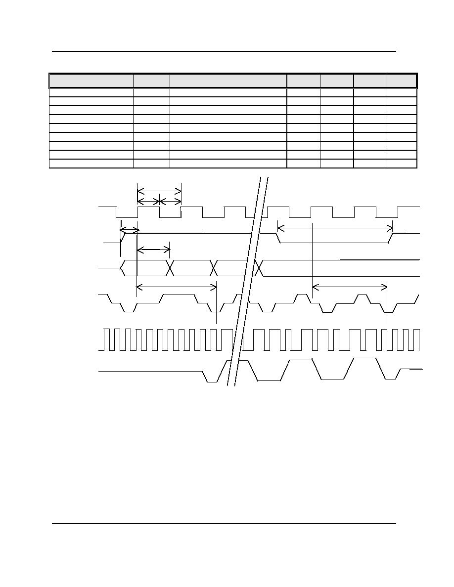
AC104QF
Ultra Low Power 10/100 Quad RMII Ethernet Transceiver
2055 Gateway Parkway Suite 700, San Jose, CA 95110 (408) 453-3700 (www.altimacom.com)
Altima Communications Inc. reserves the right to make changes to this document without notice.
Document Revision 4.0
Page 32 of 37
100Base -TX/FX & 10Base -T RMII Transmit System Timing
Parameter
SYM
Conditions
Min
Typ
Max
Units
REFCLK period
tCK
19.999
20.000
20.001
ns
REFCLK High period
tCKH
9.000
10.000
11.000
ns
REFCLK Low period
tCKL
9.000
10.000
11.000
ns
TX_EN to /J/ (SOP)
tTJ
60
-
100
ns
!TX_EN to /T/ (EOP)
tTT
60
-
100
ns
TX Propagation Delay
tTJ
From TXD[1:0] to TXOP/N(_FX)
60
-
100
ns
TXD[1:0], TX_EN Setup
tTXS
From rising edge of REFCLK
4
-
-
ns
TXD[1:0], TX_EN Hold
tTXH
From rising edge of REFCLK
0
-
2
ns
!TX_EN to TX_EN
tTX_TX
120
-
-
ns
100Base-TX/FX & 10Base -T RMII Transmit Timing
REFCLK
TX_EN
TXD[1:0]
TXOP/N
/J/
/T/
tCK
tCKH
tCKL
tTXS
tTXH
tTX_TX
tTJ
tTT
Start of Packet
End of Packet
FXTP/N
TXOP/N
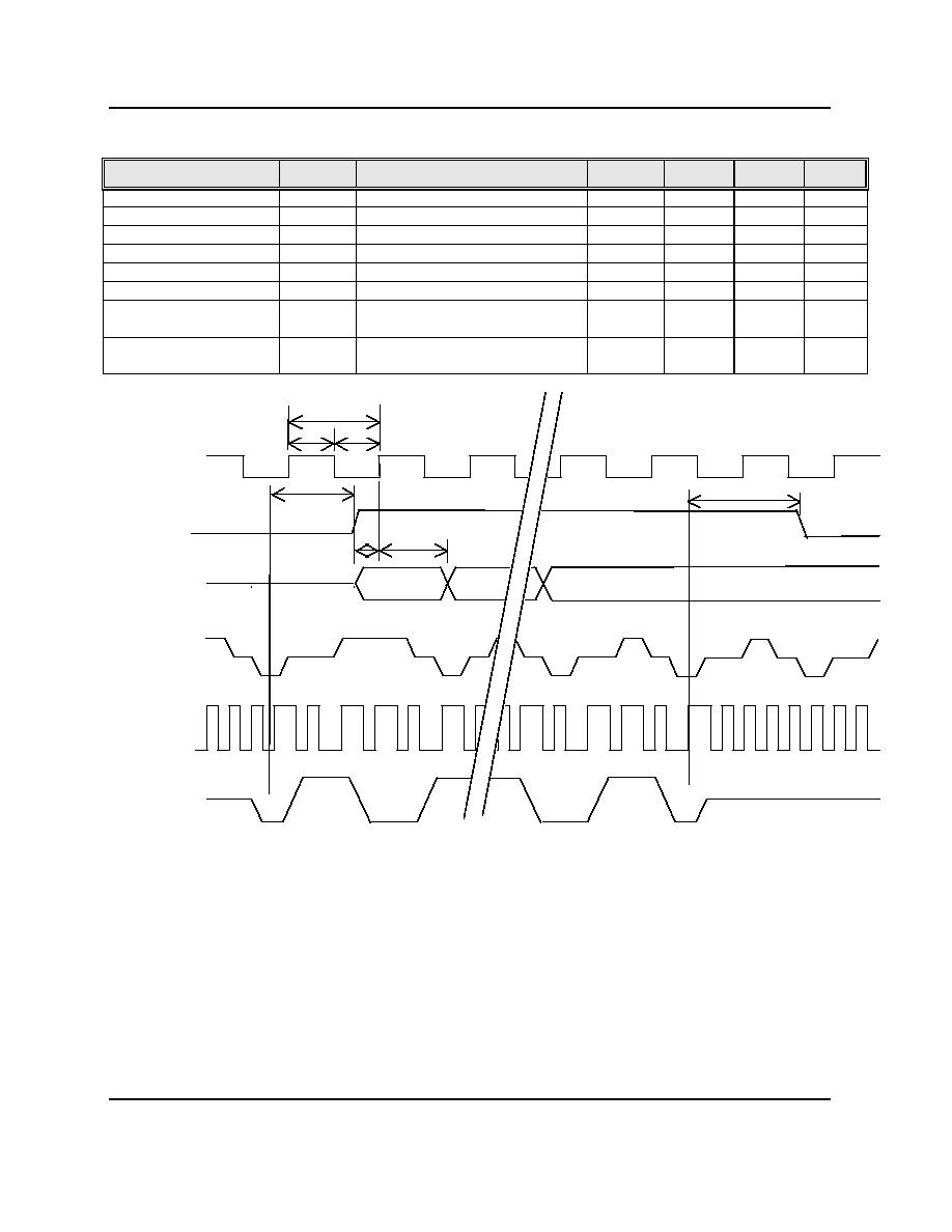
AC104QF
Ultra Low Power 10/100 Quad RMII Ethernet Transceiver
2055 Gateway Parkway Suite 700, San Jose, CA 95110 (408) 453-3700 (www.altimacom.com)
Altima Communications Inc. reserves the right to make changes to this document without notice.
Document Revision 4.0
Page 33 of 37
100Base -TX/FX & 10Base -T RMII Receive System Timing
Parameter
SYM
Conditions
Min
Typ
Max
Units
REFCLK period
tCK
19.999
20.000
20.001
ns
REFCLK High period
tCKH
9.000
10.000
11.000
ns
REFCLK Low period
tCKL
9.000
10.000
11.000
ns
/J/K (SOP) to CRS_DV
tRCSA
80
-
150
ns
/T/R (EOP) to !CRS_DV
tRCSD
120
-
190
ns
RX Propagation Delay
tRDVA
From RXIP/N(_FX) to RXD[1:0]
-
40
180
ns
RXD[1:0], CRS_DV,
RX_ER Setup
tRXS
From rising edge of REFCLK
4
-
-
ns
RXD[1:0], CRS_DV,
RX_ER Hold
tRXH
From rising edge of REFCLK
5
-
-
ns
100Base-TX/FX & 10Base-T RMII Receive Timing
REFCLK
CRS_DV
RXD[1:0]
RX_ER
RXIP/N
/J/K
/T/R
tCK
tCKH
tCKL
tRXS
tRXH
tRDVA
Start of Packet
End of Packet
tRDVD
FXRP/N
RXIP/N
SOP
EOP

AC104QF
Ultra Low Power 10/100 Quad RMII Ethernet Transceiver
2055 Gateway Parkway Suite 700, San Jose, CA 95110 (408) 453-3700 (www.altimacom.com)
Altima Communications Inc. reserves the right to make changes to this document without notice.
Document Revision 4.0
Page 34 of 37
TX APPLICATION TERMINATION
Please contact Altima Communications Inc. for the latest component value recommendation
AC104QF
TXON
TXOP
IBREF
RXIP
RXIN
1 TX+
2 TX-
3 RX+
4 Unused
5 Unused
6 RX-
7 Unused
8 Unused
RJ45
TXC_P
TX+_P
TX-_P
RX+_P
RX-_P
RXC_P
TXC_S
TX+_S
TX-_S
RX+_S
RX-_S
RXC_S
Transformer
3.3V
Chassis GND
75
X 4
110
1%
49.9
1%
49.9
1%
0.1
µ
F
0.1
µ
F
10 K
1%
1000 pF
3 KV
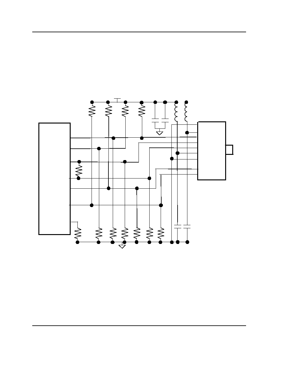
AC104QF
Ultra Low Power 10/100 Quad RMII Ethernet Transceiver
2055 Gateway Parkway Suite 700, San Jose, CA 95110 (408) 453-3700 (www.altimacom.com)
Altima Communications Inc. reserves the right to make changes to this document without notice.
Document Revision 4.0
Page 35 of 37
FX APPLICATION TERMINATION
Please contact Altima Communications Inc. for the latest component value recommendation
To enable the FX mode, FX_DIS pin must be pulled low by a 1 K
resistor.
SDP
SDN
FXRN
FXRP
FXTP
FXTN
FX_DIS
1 RXVee
2 RXVcc
3 SD
4 RD-
5 RD+
6 TXVcc
7 TXVee
8 NC
9 TD+
10 TD-
HFBR-5903
3.3V
1 K
AC104-QF
2 K
82
130
130
182
69.8
1.3 K
130
69.8
100
1 uHL
1 uHL
0.1 uF
0.1 uF
0.1 uF
10 uF
182

AC104QF
Ultra Low Power 10/100 Quad RMII Ethernet Transceiver
2055 Gateway Parkway Suite 700, San Jose, CA 95110 (408) 453-3700 (www.altimacom.com)
Altima Communications Inc. reserves the right to make changes to this document without notice.
Document Revision 4.0
Page 36 of 37
POWER AND GROUND FILTERING FOR AC104QF
Please contact Altima Communications Inc. for the latest component value recommendation.
Ground
Power
.1uf Cap
AC104QF
Components placed < 3mm
from pin
80
77
73
72
62
59
54
52
3
4
7
8
11
12
15
16
19
20
23
24
27
28
83
87
96
98
99
100
49
44
31
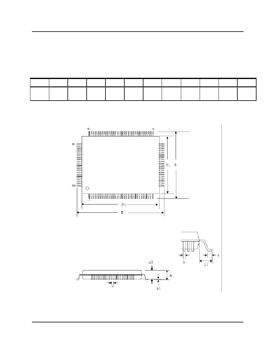
AC104QF
Ultra Low Power 10/100 Quad RMII Ethernet Transceiver
2055 Gateway Parkway Suite 700, San Jose, CA 95110 (408) 453-3700 (www.altimacom.com)
Altima Communications Inc. reserves the right to make changes to this document without notice.
Document Revision 4.0
Page 37 of 37
PACKAGE DIMENSIONS FOR AC104QF (100 PIN PQFP)
Quad Flat Pack Outline (20 x 14 mm)
N
A
A1
A2
B
D
D1
E
E1
e
L
L1
100
3.40
Max
0.25
Min
2.70
±
0.2
0.3
±
0.1
23.20
±
0.25
20.00
±
0.10
17.20
±
0.25
14.00
±
0.10
0.65
0.88
±
0.2
1.60
±
0.12