Äîêóìåíòàöèÿ è îïèñàíèÿ www.docs.chipfind.ru
MARCH 1999 - REVISED FEBRUARY 2005
Specifications are subject to change without notice.
Customers should verify actual device performance in their specific applications.
TISP7070H3SL THRU TISP7095H3SL,
TISP7125H3SL THRU TISP7220H3SL,
TISP7250H3SL THRU TISP7400H3SL
TRIPLE ELEMENT BIDIRECTIONAL THYRISTOR
OVERVOLTAGE PROTECTORS
TISP7xxxH3SL Overview
TISP7xxxH3SL Overvoltage Protector Series
Summary Electrical Characteristics
Part #
V
DRM
V
V
(BO)
V
V
T
@ I
T
V
I
DRM
µA
I
(BO)
mA
I
T
A
I
H
mA
C
o
@ -2 V
pF
Functionally
Replaces
TISP7070H3
58
70
3
5
600
5
150
140
TISP7080H3
65
80
3
5
600
5
150
140
TISP7095H3
75
95
3
5
600
5
150
140
TISP7125H3
100
125
3
5
600
5
150
74
TISP7135H3
110
135
3
5
600
5
150
74
TISP7145H3
120
145
3
5
600
5
150
74
TISP7165H3
130
165
3
5
600
5
150
74
P1553AC
TISP7180H3
145
180
3
5
600
5
150
74
TISP7200H3
150
200
3
5
600
5
150
74
P1803AC
TISP7210H3
160
210
3
5
600
5
150
74
TISP7220H3
170
220
3
5
600
5
150
74
P2103AC
TISP7250H3
200
250
3
5
600
5
150
62
P2353AC
TISP7290H3
230
290
3
5
600
5
150
62
P2703AC
TISP7300H3
230
300
3
5
600
5
150
62
TISP7350H3
275
350
3
5
600
5
150
62
P3203AC
TISP7400H3
300
400
3
5
600
5
150
62
P3403AC
Bourns' part has an improved protection voltage
Summary Current Ratings
Parameter
I
TSP
A
I
TSM
A
di/dt
A/µs
Waveshape
2/10
1.2/50, 8/20
10/160
5/320
10/560
10/1000
1 cycle 60 Hz
2/10 Wavefront
Value
500
350
250
200
130
100
60
400
This TISP® device series protects central office, access and customer premise equipment against overvoltages on the telecom line. The
TISP7xxxH3SL has the same symmetrical bidirectional protection on any terminal pair; R-T, R-G and T-G. In addition, the device is rated for
simultaneous R-G and T-G impulse conditions. The TISP7xxxH3SL is available in a wide range of voltages and has a high current capability,
allowing minimal series resistance to be used. These protectors have been specified mindful of the following standards and recommendations:
GR-1089-CORE, FCC Part 68, UL1950, EN 60950, IEC 60950, ITU-T K.20, K.21 and K.45. The TISP7350H3SL meets the FCC Part 68 "B"
ringer voltage requirement and survives both Type A and B impulse tests. These devices are housed in a through-hole 3-pin single-in-line
(SL) plastic package.
*RoHS Directive 2002/95/EC Jan 27 2003 including Annex
*RoHS COMPLIANT
VERSIONS
AVAILABLE
MARCH 1999 - REVISED FEBRUARY 2005
Specifications are subject to change without notice.
Customers should verify actual device performance in their specific applications.
Device
V
DRM
V
V
(BO)
V
`7070
58
70
`7080
65
80
`7095
75
95
`7125
100
125
`7135
110
135
`7145
120
145
`7165
130
165
`7180
145
180
`7200
150
200
`7210
160
210
`7220
170
220
`7250
200
250
`7290
230
290
`7350
275
350
`7400
300
400
ITU-T K.20/21 Rating . . . . . . . . 8 kV 10/700, 200 A 5/310
Ion-Implanted Breakdown Region
Precise and Stable Voltage
Low Voltage Overshoot under Surge
1
2
3
T
G
R
MDXXAGA
How To Order
Description
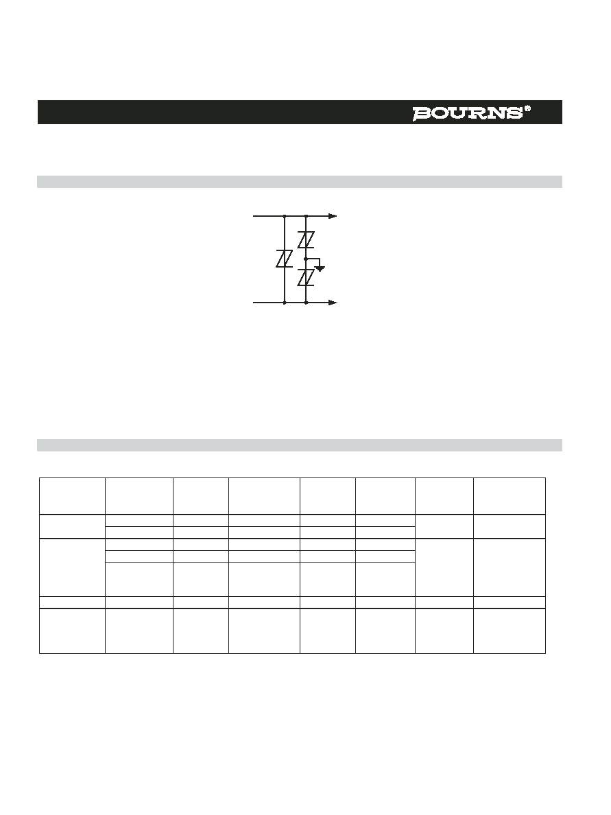
Device Symbol
SL Package (Top View)
TISP7xxxH3SL Overvoltage Protector Series
Waveshape
Standard
I
TSP
A
2/10 µs
GR-1089-CORE
500
8/20 µs
IEC 61000-4-5
350
10/160 µs
FCC Part 68
250
10/700 µs
FCC Part 68
ITU-T K.20/21
200
10/560 µs
FCC Part 68
130
10/1000 µs
GR-1089-CORE
100
Rated for International Surge Wave Shapes
- Single and Simultaneous Impulses
The TISP7xxxH3SL limits overvoltages between the telephone line Ring and Tip conductors and Ground. Overvoltages are normally caused by
a.c. power system or lightning flash disturbances which are induced or conducted on to the telephone line.
Each terminal pair, T-G, R-G and T-R, has a symmetrical voltage-triggered bidirectional thyristor protection characteristic. Overvoltages are
initially clipped by breakdown clamping until the voltage rises to the breakover level, which causes the device to crowbar into a low-voltage on
state. This low-voltage on state causes the current resulting from the overvoltage to be safely diverted through the device. The high crowbar
holding current prevents d.c. latchup as the diverted current subsides.
3-Pin Through-Hole Packaging
- Compatible with TO-220AB pin-out
-Low Height .................................................................... 8.3 mm
Low Differential Capacitance ....................................... < 72 pF
.............................................. UL Recognized Component
G
T
R
SD7XAB
Terminals T, R and G correspond to the
alternative line designators of A, B and C
Device
Package
Carrier
TISP7xxxH3
SL (Single-in-Line)
Tube
TISP7xxxH3SL
TISP7xxxH3SL-S
Insert xxx value corresponding to protection voltages of 070, 080, 095, 125 etc.
For Standard
Termination Finish
Order As
For Lead Free
Termination Finish
Order As

MARCH 1999 - REVISED FEBRUARY 2005
Specifications are subject to change without notice.
Customers should verify actual device performance in their specific applications.
Rating
Symbol
Value
Unit
Repetitive peak off-state voltage, (see Note 1)
`7070
`7080
`7095
`7125
`7135
`7145
`7165
`7180
`7200
`7210
`7220
`7250
`7290
`7350
`7400
V
DRM
± 58
± 65
± 75
±100
±110
±120
±130
±145
±150
±160
±170
±200
±230
±275
±300
V
Non-repetitive peak on-state pulse current (see Notes 2, and 3)
I
TSP
A
2/10 (Telcordia GR-1089-CORE, 2/10 voltage wave shape)
500
8/20 µs (IEC 61000-4-5, 1.2/50 µs voltage, 8/20 current combination wave generator)
350
10/160 µs (FCC Part 68, 10/160 µs voltage wave shape)
250
4/250 (ITU-T K.20/21, 10/700 voltage wave shape, dual)
225
0.2/310 (CNET I 31-24, 0.5/700 voltage wave shape)
200
5/310 (ITU-T K.20/21, 10/700 voltage wave shape, single)
200
5/320 µs (FCC Part 68, 9/720 µs voltage wave shape)
200
10/560 µs (FCC Part 68, 10/560 µs voltage wave shape)
130
10/1000 (Telcordia GR-1089-CORE, 10/1000 voltage wave shape)
100
Non-repetitive peak on-state current (see Notes 2, 3 and 4)
I
TSM
55
60
0.9
A
20 ms (50 Hz) full sine wave
16.7 ms (60 Hz) full sine wave
1000 s 50 Hz/60 Hz a.c.
Initial rate of rise of on-state current,
Exponential current ramp, Maximum ramp value < 200 A
di
T
/dt
400
A/µs
Junction temperature
T
J
-40 to +150
°C
Storage temperature range
T
stg
-65 to +150
°C
NOTES: 1. Derate value at -0.13%/°C for temperatures below 25 °C.
2. Initially the TISP7xxxH3 must be in thermal equilibrium.
3. These non-repetitive rated currents are peak values of either polarity. The rated current values may be applied to any terminal
pair. Additionally, both R and T terminals may have their rated current values applied simultaneously (in this case the G terminal
return current will be the sum of the currents applied to the R and T terminals). The surge may be repeated after the
TISP7xxxH3 returns to its initial conditions.
4. EIA/JESD51-2 environment and EIA/JESD51-3 PCB with standard footprint dimensions connected with 5 A rated printed wiring
track widths. Derate current values at -0.61 %/°C for ambient temperatures above 25 °C.
Absolute Maximum Ratings, TA = 25 °C (Unless Otherwise Noted)
TISP7xxxH3SL Overvoltage Protector Series
Description (continued)
This TISP7xxxH3SL range consists of fifteen voltage variants to meet various maximum system voltage levels (58 V to 300 V). They are
guaranteed to voltage limit and withstand the listed international lightning surges in both polarities. These high current protection devices are in
a 3-pin single-in-line (SL) plastic package and are supplied in tube pack. For alternative impulse rating, voltage and holding current values in
SL packaged protectors, consult the factory. For lower rated impulse currents in the SL package, the 45 A 10/1000 TISP7xxxF3SL series is
available.
These monolithic protection devices are fabricated in ion-implanted planar structures to ensure precise and matched breakover control and are
virtually transparent to the system in normal operation.
MARCH 1999 - REVISED FEBRUARY 2005
Specifications are subject to change without notice.
Customers should verify actual device performance in their specific applications.
Electrical Characteristics for any Terminal Pair, TA = 25 °C (Unless Otherwise Noted)
TISP7xxxH3SL Overvoltage Protector Series
Parameter
Test Conditions
Min
Typ
Max
Unit
I
DRM
Repetitive peak off-
state current
V
D
= V
DRM
T
A
= 25 °C
T
A
= 85 °C
±5
±10
µA
V
(BO)
Breakover voltage
dv/dt = ±750 V/ms, R
SOURCE
= 300
`7070
`7080
`7095
`7125
`7135
`7145
`7165
`7180
`7200
`7210
`7220
`7250
`7290
`7350
`7400
±70
±80
±95
±125
±135
±145
±165
±180
±200
±210
±220
±250
±290
±350
±400
V
V
(BO)
Impulse breakover
voltage
dv/dt ±1000 V/µs, Linear voltage ramp,
Maximum ramp value = ±500 V
di/dt = ±20 A/µs, Linear current ramp,
Maximum ramp value = ±10 A
`7070
`7080
`7095
`7125
`7135
`7145
`7165
`7180
`7200
`7210
`7220
`7250
`7290
`7350
`7400
±78
±88
±103
±134
±144
±154
±174
±189
±210
±220
±231
±261
±302
±362
±414
V
I
(BO)
Breakover current
dv/dt = ±750 V/ms, R
SOURCE
= 300
±0.1
±0.8
A
V
T
On-state voltage
I
T
= ±5 A, t
W
= 100 µs
±5
V
I
H
Holding current
I
T
= ±5 A, di/dt = - /+30 mA/ms
±0.15
±0.6
A
dv/dt
Critical rate of rise of
off-state voltage
Linear voltage ramp, Maximum ramp value < 0.85V
DRM
±5
kV/µs
I
D
Off-state current
V
D
= ±50 V
T
A
= 85 °C
±10
µA
MARCH 1999 - REVISED FEBRUARY 2005
Specifications are subject to change without notice.
Customers should verify actual device performance in their specific applications.
Electrical Characteristics for any Terminal Pair, TA = 25 °C (Unless Otherwise Noted)
C
off
Off-state capacitance
f = 1 MHz,
V
d
= 1 V rms, V
D
= 0,
f = 1 MHz,
V
d
= 1 V rms, V
D
= -1 V
f = 1 MHz,
V
d
= 1 V rms, V
D
= -2 V
f = 1 MHz,
V
d
= 1 V rms, V
D
= -50 V
f = 1 MHz,
V
d
= 1 V rms, V
D
= -100 V
(see Note 5)
`7070 thru `7095
`7125 thru `7220
`7250 thru `7400
`7070 thru `7095
`7125 thru `7220
`7250 thru `7400
`7070 thru `7095
`7125 thru `7220
`7250 thru `7400
`7070 thru `7095
`7125 thru `7220
`7250 thru `7400
`7125 thru `7220
`7250 thru `7400
170
90
84
150
79
67
140
74
62
73
35
28
33
26
pF
NOTE
5: To avoid possible voltage clipping, the `7125 is tested with V
D
= -98 V.
A
Parameter
Test Conditions
Min
Typ
Max
Unit
Thermal Characteristics
TISP7xxxH3SL Overvoltage Protector Series
Parameter
Test Conditions
Min
Typ
Max
Unit
R
JA
Junction to free air thermal resistance
EIA/JESD51-3 PCB, I
T
= I
TSM(1000)
,
T
A
= 25 °C, (see Note 6)
50
°C/W
NOTE
6: EIA/JESD51-2 environment and PCB has standard footprint dimensions connected with 5 A rated printed wiring track widths.
MARCH 1999 - REVISED FEBRUARY 2005
Specifications are subject to change without notice.
Customers should verify actual device performance in their specific applications.
Parameter Measurement Information
TISP7xxxH3SL Overvoltage Protector Series
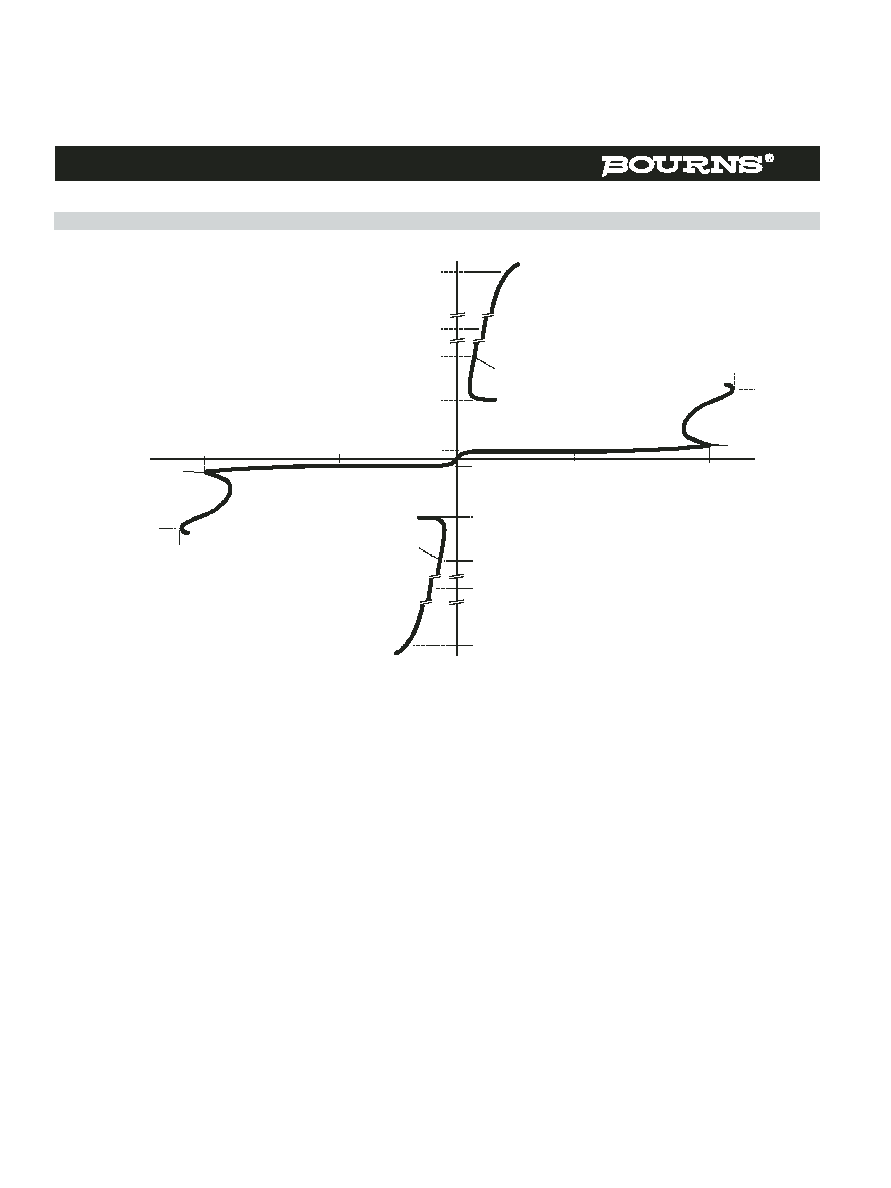
Figure 1. Voltage-current Characteristic for Terminal Pairs
-v
V
DRM
I
DRM
V
D
I
H
I
T
V
T
I
TSM
I
TSP
V
(BO)
I
(BO)
I
D
Quadrant I
Switching
Characteristic
+v
+i
V
(BO)
I
(BO)
V
D
I
D
I
H
I
T
V
T
I
TSM
I
TSP
-i
Quadrant III
Switching
Characteristic
PM4XAAC
V
DRM
I
DRM
V
D
=
±
50 V and I
D
=
±
10
µ
A
used for reliability release
MARCH 1999 - REVISED FEBRUARY 2005
Specifications are subject to change without notice.
Customers should verify actual device performance in their specific applications.
Typical Characteristics
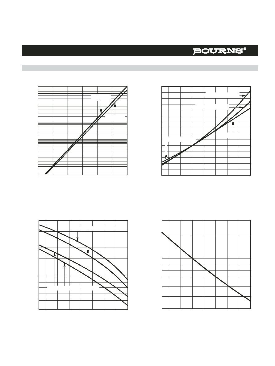
TISP7xxxH3SL Overvoltage Protector Series
Figure 2.
Figure 3.
Figure 4.
Figure 5.
T
J
- Junction Temperature -
°
C
0
25
50
75
100
125
150
|I
D
|
- Of
f-Sta
te
Cu
rr
e
n
t -
µ
A
0·0001
0·001
0·01
0·1
1
10
TC7AAA
V
D
= +50 V
V
D
= -50 V
T
J
- Junction Temperature -
°
C
-25
0
25
50
75
100
125
150
Norm
al
i
zed Breako
ver
V
o
l
t
ag
e
0.95
1.00
1.05
1.10
TC7AABA
'7070 THRU '7095
'7250 THRU '7400
'7250 THRU '7400
'7125 THRU '7220
ON-STATE CURRENT
vs
ON-STATE VOLTAGE
V
T
- On-State Voltage - V
0.7
1.5
2
3
4
5
7
1
1
0
1.5
2
3
4
5
7
15
20
30
40
50
70
150
200
1
10
100
T
A
= 25
°
C
t
W
= 100
µ
s
'3250
THRU
'3350
'3125
THRU
'3210
'3070
THRU
'3095
T
J
- Junction Temperature -
°
C
-25
0
25
50
75
100
125
150
Breakover Current Normalized to 25
°
C Holding Current
0.4
0.5
0.6
0.7
0.8
0.9
1.5
2.0
3.0
4.0
1.0
TC7AADA
+ I
(BO)
, - I
(BO)
'7250 THRU '7400
+ I
(BO)
, - I
(BO)
'7070 THRU '7220
T
J
- Junction Temperature -
°
C
-25
0
25
50
75
100
125
150
No
rm
a
l
i
z
e
d
Ho
ld
i
n
g
Cu
rr
e
n
t
0.4
0.5
0.6
0.7
0.8
0.9
1.5
2.0
1.0
TC7AAC
OFF-STATE CURRENT
vs
JUNCTION TEMPERATURE
NORMALIZED BREAKOVER CURRENT
vs
JUNCTION TEMPERATURE
NORMALIZED BREAKOVER VOLTAGE
vs
JUNCTION TEMPERATURE
NORMALIZED HOLDING CURRENT
vs
JUNCTION TEMPERATURE
MARCH 1999 - REVISED FEBRUARY 2005
Specifications are subject to change without notice.
Customers should verify actual device performance in their specific applications.
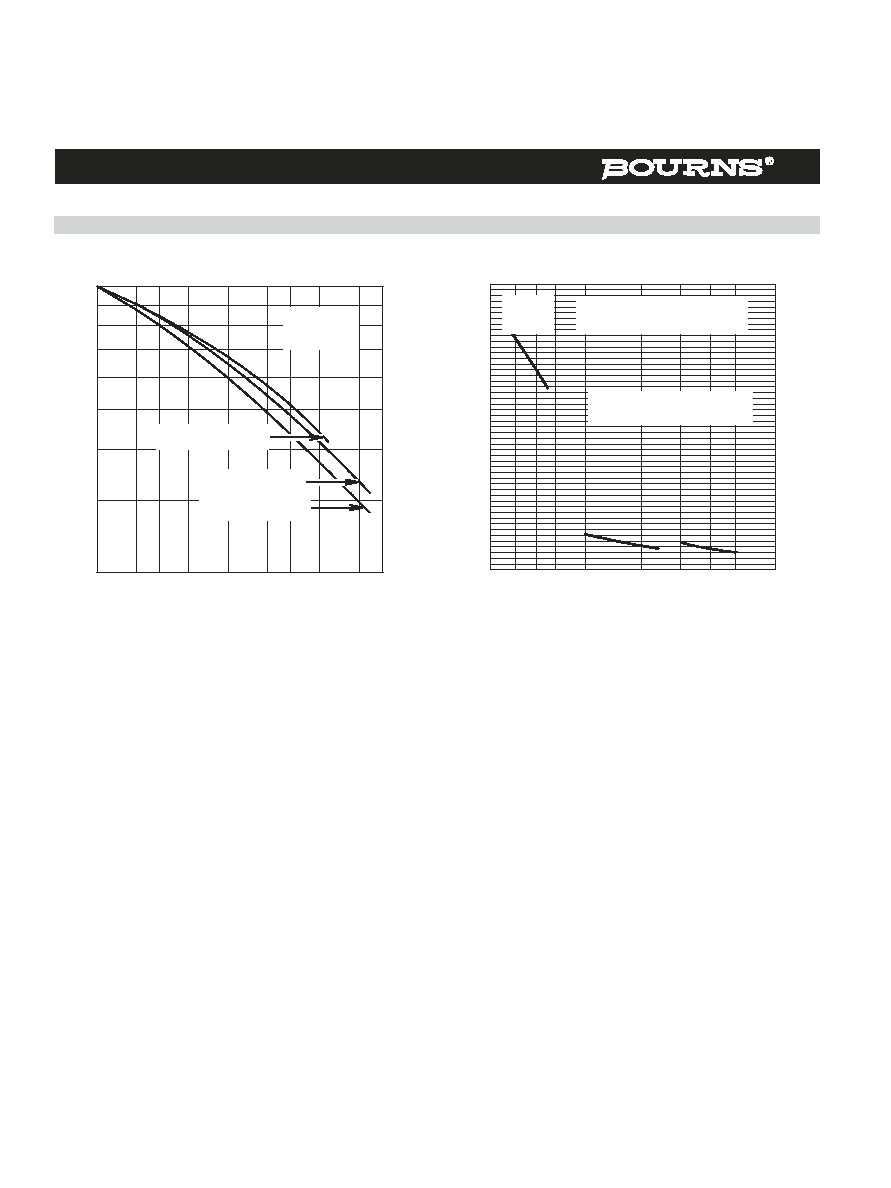
Typical Characteristics
TISP7xxxH3SL Overvoltage Protector Series
Figure 6.
Figure 7.
V
D
- Off-state Voltage - V
1
2
3
5
10
20 30
50
100 150
Capaci
t
a
n
c
e N
o
rmal
i
zed t
o
V
D
= -
1
V
0.2
0.3
0.4
0.5
0.6
0.7
0.8
0.9
1
T
J
= 25
°
C
V
d
= 1 Vrms
'7070 THRU '7095
'7250 THRU '7400
TC7AAIA
'7125 THRU '7220
V
DRM
- Repetitive Peak Off-State Voltage - V
50
60 70 80
150
200 250 300
400
100
C - Di
ff
erenti
al
Off
-S
tat
e
Cap
aci
t
a
n
ce -
p
F
30
35
40
45
50
55
60
65
70
75
80
C = C
off(-2 V)
- C
off(-50 V)
'7070
'7080
'7095
'7125
'7135
'7145
'
7180
'7250
'7290
'7350
'7210
'7400
TC
7
A
AH
A
'7220
'7165
'7200
NORMALIZED CAPACITANCE
vs
OFF-STATE VOLTAGE
DIFFERENTIAL OFF-STATE CAPACITANCE
vs
RATED REPETIVE PEAK OFF-STATE VOLTAGE
MARCH 1999 - REVISED FEBRUARY 2005
Specifications are subject to change without notice.
Customers should verify actual device performance in their specific applications.
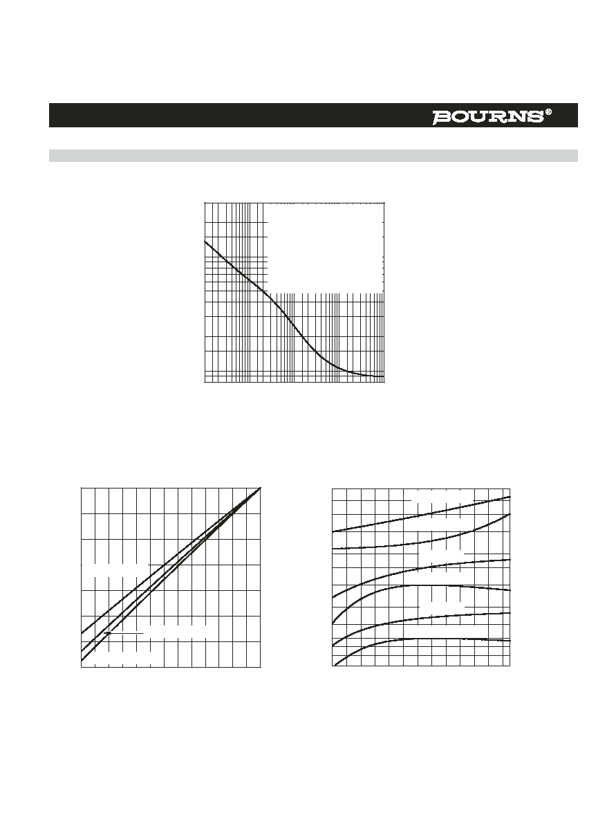
Rating and Thermal Information
TISP7xxxH3SL Overvoltage Protector Series
Figure 8.
Figure 9.
Figure 10.
t - Current Duration - s
0·1
1
10
100
1000
I
T
S
M(t)
-
Non
-
Rep
e
t
i
ti
ve P
eak O
n
-S
t
a
t
e
C
u
rrent
- A
0.8
0.9
1.5
2
3
4
5
6
7
8
9
15
20
30
1
10
TI7AB
V
GEN
= 600 V rms, 50/60 Hz
R
GEN
= 1.4*V
GEN
/I
TSM(t)
EIA/JESD51-2 ENVIRONMENT
EIA/JESD51-3 PCB, T
A
= 25
°
C
SIMULTANEOUS OPERATION
OF R AND T TERMINALS. G
TERMINAL CURRENT = 2xI
TSM(t)
T
AMIN
- Minimum Ambient Temperature -
°
C
-35
-25
-15
-5
5
15
25
-40
-30
-20
-10
0
10
20
Derat
i
n
g
Factor
0.93
0.94
0.95
0.96
0.97
0.98
0.99
1.00
'7070 THRU '7095
'7250 THRU '7400
TI7AACA
'7125 THRU '7220
T
A
- Ambient Temperature -
°
C
-40 -30 -20 -10 0
10 20 30 40 50 60 70 80
I
m
pul
se C
u
r
r
en
t
-
A
70
80
90
100
120
150
200
250
300
400
500
600
700
IEC 1.2/50, 8/20
ITU-T 10/700
FCC 10/560
FCC 10/160
TC7HAA
TELCORDIA 2/10
TELCORDIA 10/1000
NON-REPETITIVE PEAK ON-STATE CURRENT
vs
CURRENT DURATION
VDRM DERATING FACTOR
vs
MINIMUM AMBIENT TEMPERATURE
IMPULSE RATING
vs
AMBIENT TEMPERATURE
MARCH 1999 - REVISED FEBRUARY 2005
Specifications are subject to change without notice.
Customers should verify actual device performance in their specific applications.
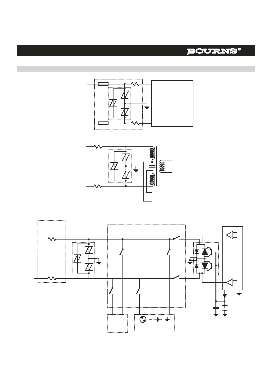
Deployment
TISP7xxxH3SL Overvoltage Protector Series
APPLICATIONS INFORMATION
Impulse Testing
These devices are three terminal overvoltage protectors. They limit the voltage between three points in the circuit. Typically, this would be the
two line conductors and protective ground (Figure 11).
In Figure 11, protectors Th2 and Th3 limit the maximum voltage between each conductor and ground to the ±V(BO) of the individual protector.
Protector Th1 limits the maximum voltage between the two conductors to its ±V(BO) value.
Manufacturers are being increasingly required to design in protection coordination. This means that each protector is operated at its design
level and currents are diverted through the appropriate protector, e.g. the primary level current through the primary protector and lower levels
of current may be diverted through the secondary or inherent equipment protection. Without coordination, primary level currents could pass
through the equipment only designed to pass secondary level currents. To ensure coordination happens with fixed voltage protectors, some
resistance is normally used between the primary and secondary protection. The values given in this data sheet apply to a 400 V (d.c.
sparkover) gas discharge tube primary protector and the appropriate test voltage when the equipment is tested with a primary protector.
To verify the withstand capability and safety of the equipment, standards require that the equipment is tested with various impulse wave forms.
The table below shows some common values.
If the impulse generator current exceeds the protector's current rating, then a series resistance can be used to reduce the current to the
protector's rated value to prevent possible failure. The required value of series resistance for a given waveform is given by the following
calculations. First, the minimum total circuit impedance is found by dividing the impulse generator's peak voltage by the protector's rated
current. The impulse generator's fictive impedance (generator's peak voltage divided by peak short circuit current) is then subtracted from the
minimum total circuit impedance to give the required value of series resistance. In some cases, the equipment will require verification over a
temperature range. By using the rated waveform values from Figure 10, the appropriate series resistor value can be calculated for ambient
temperatures in the range of -40 °C to 85 °C.
Figure 11. MULTI- POINT PROTECTION
Th3
Th2
Th1
Standard
Peak Voltage
Setting
V
Voltage
Waveform
µs
Peak Current
Value
A
Current
Waveform
µs
TISP7xxxH3
25 °C Rating
A
Series
Resistance
Coordination
Resistance
(Min.)
GR-1089-CORE
2500
2/10
500
2/10
500
0
NA
1000
10/1000
100
10/1000
100
FCC Part 68
(March 1998)
1500
10/160
200
10/160
250
0
NA
800
10/560
100
10/560
130
1000
1500
1500
9/720
(SINGLE)
(DUAL)
25
37.5
2 x 27
5/320
5/320
4/250
200
200
2 x 225
I 31-24
1500
0.5/700
37.5
0.2/310
200
0
NA
ITU-T K.20/K.21
1000
1500
4000
4000
10/700
(SINGLE)
(SINGLE)
(DUAL)
25
37.5
100
2 x 72
5/310
5/310
5/310
4/250
200
200
200
2 x 225
0
NA
NA
4.5
6.0
FCC Part 68 terminology for the waveforms produced by the ITU-T recommendation K.21 10/700 impulse generator
NA = Not Applicable, primary protection removed or not specified.

MARCH 1999 - REVISED FEBRUARY 2005
Specifications are subject to change without notice.
Customers should verify actual device performance in their specific applications.
TISP7xxxH3SL Overvoltage Protector Series
APPLICATIONS INFORMATION
AC Power Testing
Capacitance
Normal System Voltage Levels
JESD51 Thermal Measurement Method
The protector can withstand the G return currents applied for times not exceeding those shown in Figure 8. Currents that exceed these times
must be terminated or reduced to avoid protector failure. Fuses, PTC (Positive Temperature Coefficient) resistors and fusible resistors are
overcurrent protection devices which can be used to reduce the current flow. Protective fuses may range from a few hundred milliamperes to
one ampere. In some cases, it may be necessary to add some extra series resistance to prevent the fuse opening during impulse testing. The
current versus time characteristic of the overcurrent protector must be below the line shown in Figure 8. In some cases there may be a further
time limit imposed by the test standard (e.g. UL 1459 wiring simulator failure).
The protector characteristic off-state capacitance values are given for d.c. bias voltage, VD , values of 0, -1 V, -2 V and -50 V. Where possible,
values are also given for -100 V. Values for other voltages may be calculated by multiplying the VD = 0 capacitance value by the factor given in
Figure 6. Up to 10 MHz, the capacitance is essentially independent of frequency. Above 10 MHz, the effective capacitance is strongly
dependent on connection inductance. For example, a printed wiring (PW) trace of 10 cm could create a circuit resonance with the device
capacitance in the region of 50 MHz. In many applications, the typical conductor bias voltages will be about -2 V and -50 V. Figure 7 shows the
differential (line unbalance) capacitance caused by biasing one protector at -2 V and the other at -50 V.
The protector should not clip or limit the voltages that occur in normal system operation. For unusual conditions, such as ringing without the
line connected, some degree of clipping is permissible. Under this condition, about 10 V of clipping is normally possible without activating the
ring trip circuit.
Figure 9 allows the calculation of the protector VDRM value at temperatures below 25 °C. The calculated value should not be less than the
maximum normal system voltages. The TISP7290H3, with a VDRM of 230 V, can be used for the protection of ring generators producing
105 V rms of ring on a battery voltage of -58 V. The peak ring voltage will be 58 + 1.414*105 = 206.5 V. However, this is the open circuit voltage
and the connection of the line and its equipment will reduce the peak voltage.
For the extreme case of an unconnected line, the temperature at which clipping begins can be calculated using the data from Figure 9. To
possibly clip, the VDRM value has to be 206.5 V. This is a reduction of the 230 V 25 °C VDRM value by a factor of 206.5/230 = 0.90. Figure 9
shows that a 0.90 reduction will occur below an ambient temperature of -40 °C. For this example, the TISP7290H3 will allow normal equipment
operation, even on an open-circuit line, down to below -40 °C
.
To standardize thermal measurements, the EIA (Electronic Industries Alliance) has created the JESD51 standard. Part 2 of the standard
(JESD51-2, 1995) describes the test environment. This is a 0.0283 m3 (1 ft3) cube which contains the test PCB (Printed Circuit Board)
horizontally mounted at the center. Part 3 of the standard (JESD51-3, 1996) defines two test PCBs for surface mount components; one for
packages smaller than 27 mm (1.06 '') on a side and the other for packages up to 48 mm (189 ''). The thermal measurements used the smaller
76.2 mm x 114.3 mm (3.0 '' x 4.5 '') PCB. The JESD51-3 PCBs are designed to have low effective thermal conductivity (high thermal resis-
tance) and represent a worse case condition. The PCBs used in the majority of applications will achieve lower values of thermal resistance and
so can dissipate higher power levels than indicated by the JESD51 values.
MARCH 1999 - REVISED FEBRUARY 2005
Specifications are subject to change without notice.
Customers should verify actual device performance in their specific applications.
TISP7xxxH3SL Overvoltage Protector Series
Typical Circuits
Figure 12. Protection Module
Figure 13. ISDN Protection
Figure 14. Line Card Ring/Test Protection
PROTECTED
EQUIPMENT
E.G. LINE CARD
AI7XBK
Th3
Th2
Th1
TISP7xxxH3
R1a
R1b
RING
WIRE
TIP
WIRE
F1a
F1b
R1a
R1b
AI7XBL
SIGNAL
D.C.
Th3
Th2
Th1
TISP7150H3
TEST
RELAY
RING
RELAY
SLIC
RELAY
TEST
EQUIP-
MENT
RING
GENERATOR
S1a
S1b
R1a
R1b
RING
WIRE
TIP
WIRE
Th3
Th2
Th1
Th4
Th5
SLIC
SLIC
PROTECTION
RING/TEST
PROTECTION
OVER-
CURRENT
PROTECTION
S2a
S2b
S3a
S3b
V
BAT
C1
220 nF
AI7XBJ
TISP6xxxx,
TISPPBLx,
1/2 TISP6NTP2
COORDI-
NATION
RESISTANCE
TISP7xxxH3
MARCH 1999 - REVISED FEBRUARY 2005
Specifications are subject to change without notice.
Customers should verify actual device performance in their specific applications.
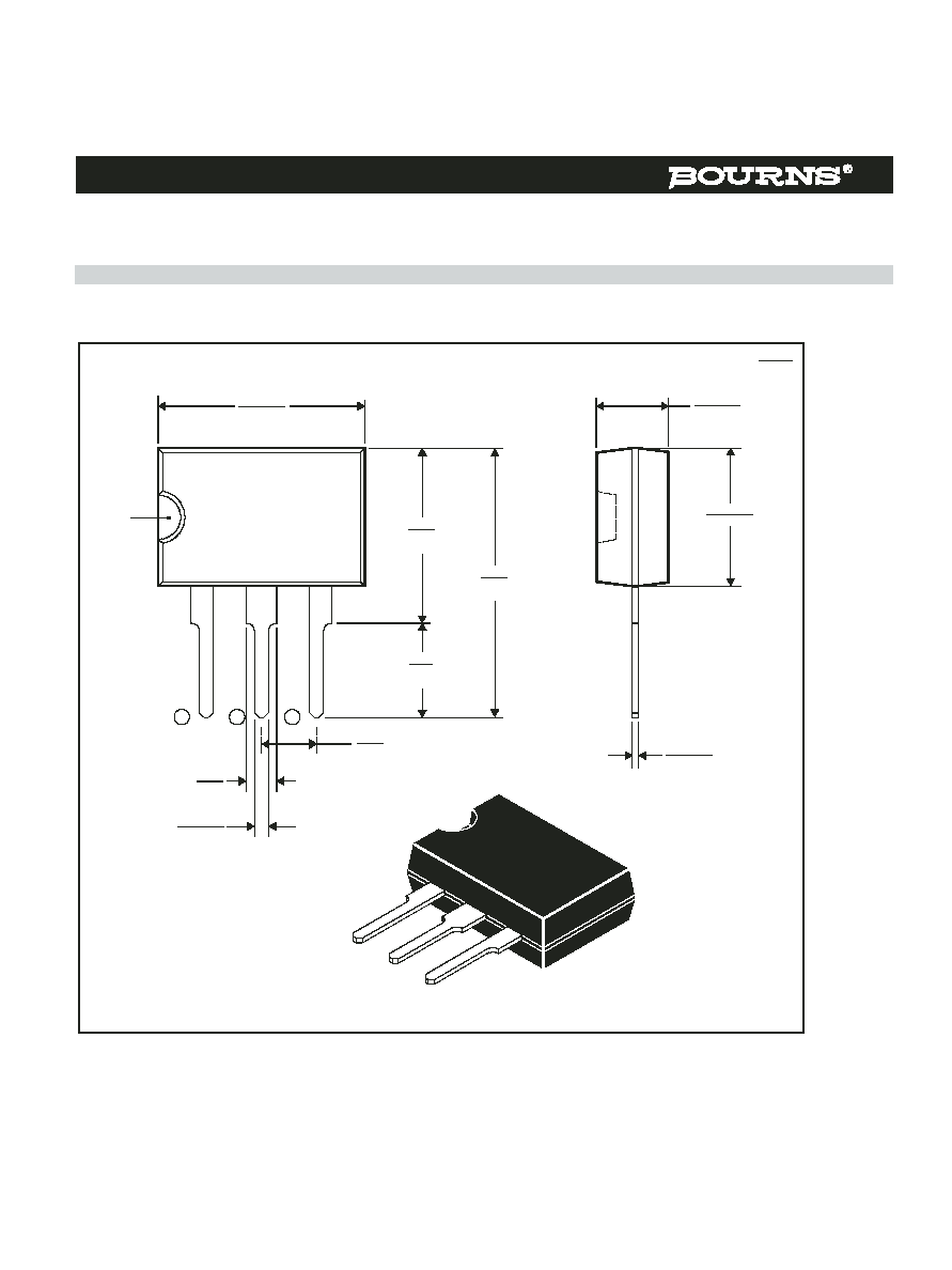
MECHANICAL DATA
TISP7xxxH3SL Overvoltage Protector Series
SL003 3-pin Plastic Single-in-line Package
This single-in-line package consists of a circuit mounted on a lead frame and encapsulated within a plastic compound. The compound will
withstand soldering temperature with no deformation, and circuit performance characteristics will remain stable when operated in high
humidity conditions. Leads require no additional cleaning or processing when used in soldered assembly.
"TISP" is a trademark of Bourns, Ltd., a Bourns Company, and is Registered in U.S. Patent and Trademark Office.
"Bourns" is a registered trademark of Bourns, Inc. in the U.S. and other countries.
SL003
2
1
3
NOTES: A. Each pin centerline is located within 0.25 (0.010) of its true longitudinal position.
B. Body molding flash of up to 0.15 (0.006) may occur in the package lead plane.
MDXXCE
Index
Notch
9.25 - 9.75
(0.364 - 0.384)
3.20 - 3.40
(0.126 - 0.134)
6.10 - 6.60
(0.240- 0.260)
0.203 - 0.356
(0.008- 0.014)
0.559 - 0.711
(0.022 - 0.028)
3 Places
12.9
(0.492)
DIMENSIONS ARE:
METRIC
(INCHES)
4.267
(0.168)
MIN.
MAX.
1.854
(0.073)
MAX.
8.31
(0.327)
MAX.
2.54
(0.100)
Typical
(See Note A)
2 Places