
NOVEMBER 1997 - REVISED FEBRUARY 2005
Specifications are subject to change without notice.
Customers should verify actual device performance in their specific applications.
TISP4xxxM3LM Overvoltage Protector Series
TISP4070M3LM THRU TISP4115M3LM,
TISP4125M3LM THRU TISP4220M3LM,
TISP4240M3LM THRU TISP4400M3LM
BIDIRECTIONAL THYRISTOR OVERVOLTAGE PROTECTORS
Summary Current Ratings
Summary Electrical Characteristics
TISP4xxxM3LM Overview
This TISP® device series protects central office, access and customer premise equipment against overvoltages on the telecom line. The
TISP4xxxM3LM is available in a wide range of voltages and has a medium current capability. These protectors have been specified mindful of
the following standards and recommendations: GR-1089-CORE, FCC Part 68, UL1950, EN 60950, IEC 60950, ITU-T K.20, K.21 and K.45. The
TISP4350M3LM meets the FCC Part 68 "B" ringer voltage requirement and survives the Type B impulse tests. These devices are housed in a
through-hole DO-92 package (TO-92 package with cropped center leg).
Part #
V
DRM
V
V
(BO)
V
V
T
@ I
T
V
I
DRM
µA
I
(BO)
mA
I
T
A
I
H
mA
C
o
@ -2 V
pF
Functionally
Replaces
TISP4070M3
58
70
3
5
600
5
150
120
P0640EA
TISP4080M3
65
80
3
5
600
5
150
120
P0720EA
TISP4095M3
75
95
3
5
600
5
150
120
P0900EA
TISP4115M3
90
115
3
5
600
5
150
120
P1100EA
TISP4125M3
100
125
3
5
600
5
150
65
TISP4145M3
120
145
3
5
600
5
150
65
P1300EA
TISP4165M3
135
165
3
5
600
5
150
65
TISP4180M3
145
180
3
5
600
5
150
65
P1500EA
TISP4220M3
160
220
3
5
600
5
150
65
P1800EA
TISP4240M3
180
240
3
5
600
5
150
55
TISP4250M3
190
250
3
5
600
5
150
55
P2300EA
TISP4260M3
200
260
3
5
600
5
150
55
TISP4290M3
220
290
3
5
600
5
150
55
P2600EA
TISP4300M3
230
300
3
5
600
5
150
55
TISP4350M3
275
350
3
5
600
5
150
55
P3100EA
TISP4395M3
320
395
3
5
600
5
150
55
P3500EA
TISP4400M3
300
400
3
5
600
5
150
55
B ourns' part has an improved protection voltage
Parameter
I
TSP
A
I
TSM
A
di/dt
A/µs
Waveshape
2/10
1.2/50, 8/20
10/160
5/320
10/560
10/1000
1 cycle 60 Hz
2/10 Wavefront
Value
300
220
120
100
75
50
32
300
*RoHS Directive 2002/95/EC Jan 27 2003 including Annex
*RoHS COMPLIANT
VERSIONS
AVAILABLE
NOVEMBER 1997 - REVISED FEBRUARY 2005
Specifications are subject to change without notice.
Customers should verify actual device performance in their specific applications.
T
R
SD4XAA
Terminals T and R correspond to the
alternative line designators of A and B
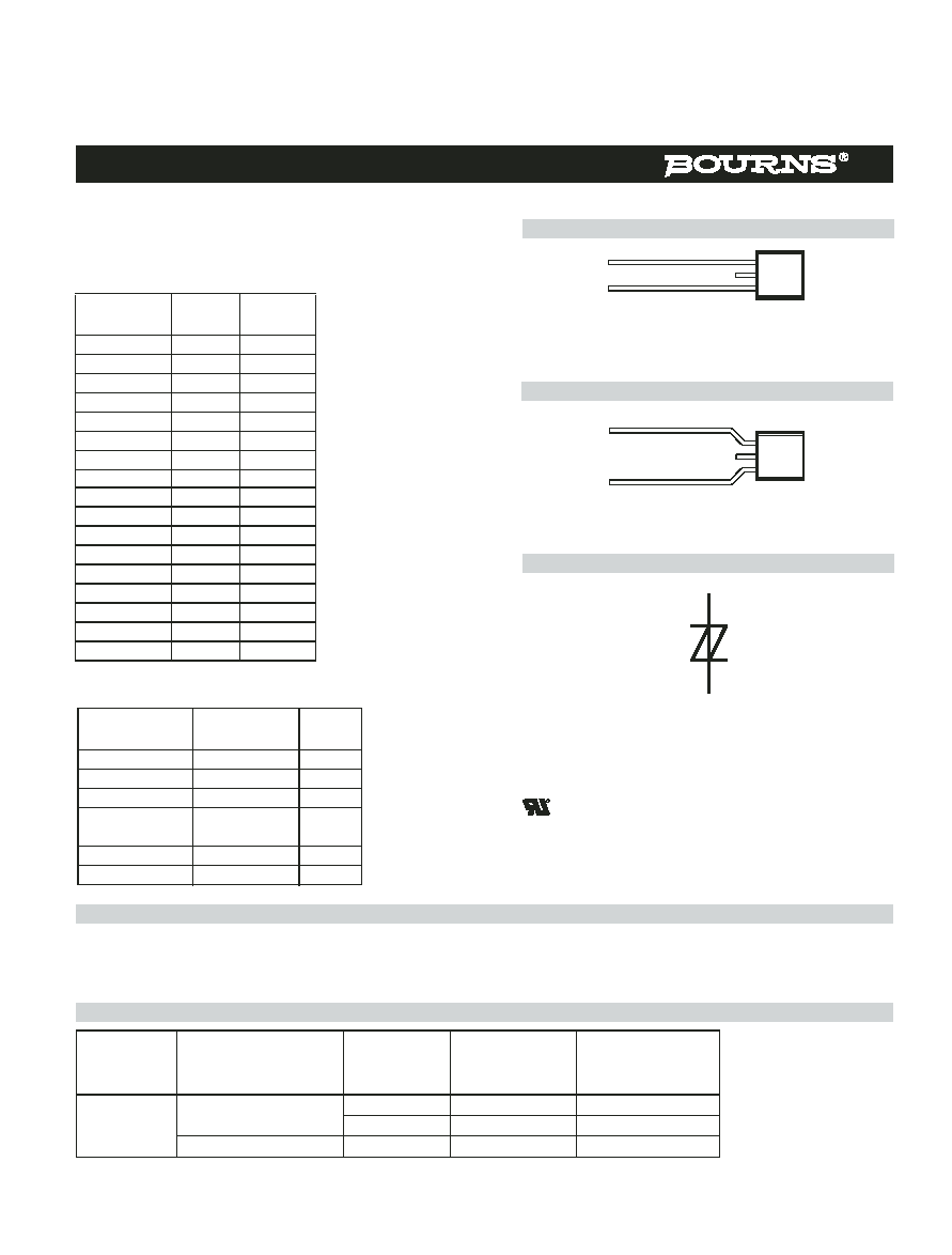
LMF Package (LM Package with Formed Leads) (Top View)
Waveshape
Standard
I
TSP
A
2/10 µs
GR-1089-CORE
300
8/20 µs
IEC 61000-4-5
220
10/160 µs
FCC Part 68
120
10/700 µs
ITU-T K.20/21
FCC Part 68
100
10/560 µs
FCC Part 68
75
10/1000 µs
GR-1089-CORE
50
How To Order
LM Package (Top View)
Ion-Implanted Breakdown Region
Precise and Stable Voltage
Low Voltage Overshoot under Surge
Rated for International Surge Wave Shapes
Device Symbol
Description
TISP4xxxM3LM Overvoltage Protector Series
ITU-T K.20/21 Rating ...........................4 kV 10/700,100 A 5/310
These devices are designed to limit overvoltages on the telephone line. Overvoltages are normally caused by a.c. power system or lightning
flash disturbances which are induced or conducted on to the telephone line. A single device provides 2-point protection and is typically used
for the protection of 2-wire telecommunication equipment (e.g. between the Ring and Tip wires for telephones and modems). Combinations of
devices can be used for multi-point protection (e.g. 3-point protection between Ring, Tip and Ground).
Low Differential Capacitance .................................. 43 pF max.
.............................................. UL Recognized Component
NC - No internal connection on pin 2
NC
T(A)
R(B)
MD4XAT
1
2
3
NC - No internal connection on pin 2
NC
T(A)
R(B)
MD4XAKB
1
2
3
Device
Package
Carrier
TISP4xxxM3LM
Straight Lead DO-92 (LM)
Bulk Pack
TISP4xxxM3LM
Tape and Reeled
TISP4xxxM3LMR
Formed Lead DO-92 (LMF)
Tape and Reeled TISP4xxxM3LMFR
TISP4xxxM3LM-S
TISP4xxxM3LMR-S
TISP4xxxM3LMFRS
Insert xxx value corresponding to protection voltages of 070, 080, 095, 115 etc.
For Standard
Termination Finish
Order As
For Lead Free
Termination Finish
Order As
Device
V
DRM
V
V
(BO)
V
`4070
58
70
`4080
65
80
`4095
75
95
`4115
90
115
`4125
100
125
`4145
120
145
`4165
135
165
`4180
145
180
`4220
160
220
`4240
180
240
`4250
190
250
`4260
200
260
`4290
220
290
`4300
230
300
`4350
275
350
`4395
320
395
`4400
300
400

NOVEMBER 1997 - REVISED FEBRUARY 2005
Specifications are subject to change without notice.
Customers should verify actual device performance in their specific applications.
Description (continued)
TISP4xxxM3LM Overvoltage Protector Series
Rating
Symbol
Value
Unit
Repetitive peak off-state voltage, (see Note 1)
`4070
`4080
`4095
`4115
`4125
`4145
`4165
`4180
`4220
`4240
`4250
`4260
`4290
`4300
`4350
`4395
`4400
V
DRM
± 58
± 65
± 75
± 90
±100
±120
±135
±145
±160
±180
±190
±200
±220
±230
±275
±320
±300
V
Non-repetitive peak on-state pulse current (see Notes 2, 3 and 4)
I
TSP
A
2/10 µs (GR-1089-CORE, 2/10 µs voltage wave shape)
300
8/20 µs (IEC 61000-4-5, combination wave generator, 1.2/50 voltage, 8/20 current)
220
10/160 µs (FCC Part 68, 10/160 µs voltage wave shape)
120
5/200 µs (VDE 0433, 10/700 µs voltage wave shape)
110
0.2/310 µs (I 31-24, 0.5/700 µs voltage wave shape)
100
5/310 µs (ITU-T K.20/21, 10/700 µs voltage wave shape)
100
5/310 µs (FTZ R12, 10/700 µs voltage wave shape)
100
5/320 µs (FCC Part 68, 9/720 µs voltage wave shape)
100
10/560 µs (FCC Part 68, 10/560 µs voltage wave shape)
75
10/1000 µs (GR-1089-CORE, 10/1000 µs voltage wave shape)
50
Non-repetitive peak on-state current (see Notes 2, 3 and 5)
I
TSM
30
32
2.1
A
20 ms (50 Hz) full sine wave
16.7 ms (60 Hz) full sine wave
1000 s 50 Hz/60 Hz a.c.
Initial rate of rise of on-state current,
Exponential current ramp, Maximum ramp value < 100 A
di
T
/dt
300
A/µs
Junction temperature
T
J
-40 to +150
°C
Storage temperature range
T
stg
-65 to +150
°C
NOTES: 1. See Applications Information and Figure 10 for voltage values at lower temperatures.
2. Initially the TISP4xxxM3LM must be in thermal equilibrium with T
J
= 25 °C.
3. The surge may be repeated after the TISP4xxxM3LM returns to its initial conditions.
4. See Applications Information and Figure 11 for current ratings at other temperatures.
5. EIA/JESD51-2 environment and EIA/JESD51-3 PCB with standard footprint dimensions connected with 5 A rated printed wiring
track widths. See Figure 8 for the current ratings at other durations. Derate current values at -0.61 %/°C for ambient
temperatures above 25 °C
Absolute Maximum Ratings, TA = 25 °C (Unless Otherwise Noted)
The protector consists of a symmetrical voltage-triggered bidirectional thyristor. Overvoltages are initially clipped by breakdown clamping until
the voltage rises to the breakover level, which causes the device to crowbar into a low-voltage on state. This low-voltage on state causes the
current resulting from the overvoltage to be safely diverted through the device. The high crowbar holding current prevents d.c. latchup as the
diverted current subsides.
This TISP4xxxM3LM range consists of seventeen voltage variants to meet various maximum system voltage levels (58 V to 320 V). They are
guaranteed to voltage limit and withstand the listed international lightning surges in both polarities. These protection devices are supplied in a
DO-92 (LM) cylindrical plastic package. The TISP4xxxM3LM is a straight lead DO-92 supplied in bulk pack and on tape and reel. The
TISP4xxxM3LMF is a formed lead DO-92 supplied only on tape and reel. For higher rated impulse currents in the DO-92 package, the 100 A
10/1000 TISP4xxxH3LM series is available.
NOVEMBER 1997 - REVISED FEBRUARY 2005
Specifications are subject to change without notice.
Customers should verify actual device performance in their specific applications.
Parameter
Test Conditions
Min
Typ
Max
Unit
I
DRM
Repetitive peak off-
state current
V
D
= ±V
DRM
T
A
= 25 °C
T
A
= 85 °C
±5
±10
µA
V
(BO)
Breakover voltage
dv/dt = ±750 V/ms, R
SOURCE
= 300
`4070
`4080
`4095
`4115
`4125
`4145
`4165
`4180
`4220
`4240
`4250
`4260
`4290
`4300
`4350
`4395
`4400
±70
±80
±95
±115
±125
±145
±165
±180
±220
±240
±250
±260
±290
±300
±350
±395
±400
V
V
(BO)
Impulse breakover
voltage
dv/dt
±1000 V/µs, Linear voltage ramp,
Maximum ramp value = ±500 V
di/dt = ±20 A/µs, Linear current ramp,
Maximum ramp value = ±10 A
`4070
`4080
`4095
`4115
`4125
`4145
`4165
`4180
`4220
`4240
`4250
`4260
`4290
`4300
`4350
`4395
`4400
±78
±88
±102
±122
±132
±151
±171
±186
±227
±247
±257
±267
±298
±308
±359
±405
±410
V
I
(BO)
Breakover current
dv/dt = ±750 V/ms, R
SOURCE
= 300
±0.15
±0.6
A
V
T
On-state voltage
I
T
= ±5 A, t
W
= 100 µs
±3
V
I
H
Holding current
I
T
= ±5 A, di/dt = - /+ 3 0 mA/ms
±0.15
±0.6
A
dv/dt
Critical rate of rise of
off-state voltage
Linear voltage ramp, Maximum ramp value < 0.85V
DRM
±5
kV/µs
I
D
Off-state current
V
D
= ±50 V
T
A
= 85 °C
±10
µA
Electrical Characteristics, TA = 25 °C (Unless Otherwise Noted)
TISP4xxxM3LM Overvoltage Protector Series

NOVEMBER 1997 - REVISED FEBRUARY 2005
Specifications are subject to change without notice.
Customers should verify actual device performance in their specific applications.
Parameter
Test Conditions
Min
Typ
Max
Unit
R
JA
Junction to free air thermal resistance
EIA/JESD51-3 PCB, I
T
= I
TSM(1000)
,
T
A
= 25 °C, (see Note 7)
120
°C/W
265 mm x 210 mm populated line card,
4-layer PCB, I
T
= I
TSM(1000)
, T
A
= 25 °C
57
NOTE
7: EIA/JESD51-2 environment and PCB has standard footprint dimensions connected with 5 A rated printed wiring track widths.
Thermal Characteristics
TISP4xxxM3LM Overvoltage Protector Series
Electrical Characteristics, TA = 25 °C (Unless Otherwise Noted) (continued)
C
off
Off-state capacitance
f = 100 kHz,
V
d
= 1 V rms, V
D
= 0,
f = 100 kHz,
V
d
= 1 V rms, V
D
= -1 V
f = 100 kHz,
V
d
= 1 V rms, V
D
= -2 V
f = 100 kHz,
V
d
= 1 V rms, V
D
= -50 V
f = 100 kHz,
V
d
= 1 V rms, V
D
= -100 V
(see Note 6)
4070 thru `4115
`4125 thru `4220
`4240 thru `4400
`4070 thru `4115
`4125 thru `4220
`4240 thru `4400
`4070 thru `4115
`4125 thru `4220
`4240 thru `4400
`4070 thru `4115
`4125 thru `4220
`4240 thru `4400
`4125 thru `4220
`4240 thru `4400
86
60
54
80
56
50
74
52
46
36
26
20
20
16
110
80
70
96
74
64
90
70
60
47
36
30
30
24
pF
NOTE
6: To avoid possible voltage clipping, the `4125 is tested with V
D
= -98 V.
Parameter
Test Conditions
Min
Typ
Max
Unit