
SRAM
SRAM
SRAM
SRAM
SRAM
AS5LC1008
Austin Semiconductor, Inc.
AS5LC1008
Rev. 1.0 11/02
Austin Semiconductor, Inc. reserves the right to change products or specifications without notice.
1
FEATURES
· High-speed access times of 10, 12, 15 and 20 ns
· High-performance, low-power CMOS process
· Multiple center power and ground pins for greater noise
immunity
· Easy memory expansion with CE\ and OE\ options
· CE\ power-down
· Fully static operation: no clock or refresh required
· TTL compatible inputs and outputs
· Single 3.3V power supply
128K x 8 SRAM
High-Speed CMOS SRAM with
3.3V Revolutionary Pinout
PIN ASSIGNMENT
(Top View)
32-Pin, 400-mil
Plastic SOJ (DJ) & Ceramic SOJ (DCJ)
GENERAL DESCRIPTION
The ASI AS5LC1008 is a very high-speed, low power,
131,072-word by 8-bit CMOS static RAM in revolutionary
pinout. The AS5LC1008 is fabricated using high-performance
CMOS technology. This highly reliable process coupled with
innovative circuit design techniques, yields higher performance
and low power consumption devices.
When CE\ is HIGH (deselected), the device assumes a
standby mode at which the power dissipation can be reduced
down to 250µW (typical) with CMOS input levels.
The AS5LC1008 operates from a single 3.3V power supply
and all inputs are TTL-compatible.
OPTIONS
MARKING
· Timing
10ns access
-10
12ns access
-12
15ns access
-15
20ns access
-20
· Package
Plastic SOJ (32-pin, 400-mil)
DJ No. 906
*Ceramic SOJ (32-pin, 400-mil)
DCJ No. 501
· Operating Temperature Ranges
-Military (-55
o
C to +125
o
C)
XT
-Industrial (-40
o
C to +85
o
C)
IT
*Consult Factory, Possible Future Offering
For more products and information
please visit our web site at
www.austinsemiconductor.com
PIN FUNCTIONS
1
2
3
4
5
6
7
8
9
1 0
1 1
1 2
1 3
1 4
1 5
1 6
A0
A1
A2
A3
CE\
I/O 0
I/O 1
Vcc
GND
I/O 2
I/O 3
WE\
A4
A5
A6
A7
3 2
3 1
3 0
2 9
2 8
2 7
2 6
2 5
2 4
2 3
2 2
2 1
2 0
1 9
1 8
1 7
A16
A15
A14
A13
OE\
I/O 7
I/O 6
GND
Vcc
I/O 5
I/O 4
A12
A11
A10
A9
A8
PIN DESCRIPTION
A0 - A16
Address Inputs
CE\
Chip Enable Input
OE\
Output Enable Input
WE\
Write Enable Input
I/O0 - I/O7
Bidirectional Ports
V
CC
Power
GND
Ground

SRAM
SRAM
SRAM
SRAM
SRAM
AS5LC1008
Austin Semiconductor, Inc.
AS5LC1008
Rev. 1.0 11/02
Austin Semiconductor, Inc. reserves the right to change products or specifications without notice.
2
ABSOLUTE MAXIMUM RATINGS*
Terminal Voltage with Respect to GND (V
TERM
)...........................................................................................-0.5V to V
CC
+ 0.5V
Temperature Under Bias (T
BIAS
).............................................................................................................................-55°C to +125°C
Storage Temperature (T
STG
)....................................................................................................................................-65°C to +150°C
Power Dissipation (P
T
)................................................................................................................................................................1.0W
*Stresses greater than those listed under "Absolute Maximum Ratings" may cause permanent damage to the device. This is a stress rating only and functional
operation of the device at these or any other conditions above those indicated in the operation section of this specification is not implied. Exposure to absolute
maximum rating conditions for extended periods may affect reliability.
FUNCTIONAL BLOCK DIAGRAM
TRUTH TABLE
Mode
WE\
CE\
OE\
I/O Operation V
CC
Current
Not Selected
(Power-down)
X
H
X
High-Z
I
SB1
, I
SB2
Output Disabled
H
L
H
High-Z
I
CC1
, I
CC2
Read
H
L
L
D
OUT
I
CC1
, I
CC2
Write
L
L
X
D
IN
I
CC1
, I
CC2
A0 - A16
V
CC
GND
I/O0 - I/O7
CE\
OE\
WE\
DECODER
128K x 8
MEMORY ARRAY
I/O DATA
CIRCUIT
COLUMN I/O
CONTROL
CIRCUIT

SRAM
SRAM
SRAM
SRAM
SRAM
AS5LC1008
Austin Semiconductor, Inc.
AS5LC1008
Rev. 1.0 11/02
Austin Semiconductor, Inc. reserves the right to change products or specifications without notice.
3
ELECTRICAL CHARACTERISTICS AND RECOMMENDED DC OPERATING CONDITIONS
(-55
o
C < T
A
< +125
o
C or -40
o
C to +85
o
C; Vcc = 3.3V +0.3V)
PARAMETER
SYMBOL
CONDITIONS
MIN
MAX
UNITS
Output HIGH Voltage
V
OH
V
CC
= Min., I
OH
= -4.0mA
2.4
---
V
Output LOW Voltage
V
OL
V
CC
= Min., I
OL
= 8.0mA
---
0.4
V
Input HIGH Voltage
V
IH
2.2
V
CC
+ 0.3
V
Input LOW Voltage
1
V
IL
-0.3
0.8
V
Input Leakage
I
LI
GND < V
IN
< V
CC
-5
5
µA
Output Leakage
I
LO
GND < V
OUT
< V
CC
;
Outputs Disabled
-5
5
µA
NOTE:
1. V
IL
= -3.0V for pulse width less than 10ns.
POWER SUPPLY CHARACTERISTICS
1
(-55
o
C < T
A
< +125
o
C or -40
o
C to +85
o
C; Vcc = 3.3V +0.3V)
NOTE:
1. At f = f
MAX
, address and data inputs are cycling at the maximum frequency, f = 0 means no input lines change.
CAPACITANCE
1,2
PARAMETER
SYMBOL CONDITIONS
MAX
UNIT
Input Capacitance
C
IN
V
IN
= 0V
6
pF
Input/Output Capacitance
C
I/O
V
OUT
= 0V
8
pF
NOTE:
1. Tested initially and after any design or process changes that may affect these parameters.
2. Test conditions: T
A
= 25°C, f = 1MHz, V
CC
= 3.3V.
PARAMETER
SYM
CONDITIONS
MIN MAX MIN MAX MIN MAX MIN MAX UNIT
V
CC
Dynamic Operating
Supply Current
I
CC
V
CC
= Max, CE\ = V
IL
,
I
OUT
= 0 mA, f = Max
---
160
---
140
---
130
---
120
mA
I
SB
V
CC
= Max, V
IN
= V
IH
or V
IL
CE\ > V
IH
, f = Max
---
45
---
40
---
35
---
30
mA
I
SB1
V
CC
= Max, V
IN
= V
IH
or V
IL
CE\ > V
IH
, f = 0
---
30
---
30
---
30
---
30
mA
CMOS Standby Current
(CMOS Inputs)
I
SB2
V
IN
> V
CC
- 0.2V,
or V
IN
< 0.2V, f = 0
---
10
---
10
---
10
---
10
mA
-10
-12
-20
TTL Standby Current
(TTL Inputs)
-15

SRAM
SRAM
SRAM
SRAM
SRAM
AS5LC1008
Austin Semiconductor, Inc.
AS5LC1008
Rev. 1.0 11/02
Austin Semiconductor, Inc. reserves the right to change products or specifications without notice.
4
READ CYCLE SWITCHING CHARACTERISTICS
1
(-55
o
C < T
A
< +125
o
C or -40
o
C to +85
o
C; Vcc = 3.3V +0.3V)
NOTES:
1. Test conditions assume signal transition times of 3ns or less, timing reference levels of 1.5V, input pulse levels of 0 to 3.0V and C1 output loading specified
in Figure 1.
2. Tested with the C2 load in Figure 1. Transition is measured ±500 mV from steady-state voltage. Not 100% tested.
AC TEST CONDITIONS
PARAMETER
UNIT
Input Pulse Level
0V to 3.0V
Input Rise and Fall Times
3ns
Input and Output timing and Reference Levels
1.5V
Output Load
See Figures 1 and 2
FIGURE 1
FIGURE 2
AC TEST LOADS
PARAMETER
SYMBOL
MIN
MAX
MIN
MAX
MIN
MAX
MIN
MAX
UNIT
Read Cycle Time
t
RC
10
---
12
---
15
---
20
---
ns
Address Access Time
t
AA
---
10
---
12
---
15
---
20
ns
Output Hold time
t
OHA
2
---
2
---
2
---
2
---
ns
CE\ Access Time
t
ACE
---
10
---
12
---
15
---
20
ns
OE\ Access Time
t
DOE
---
5
---
6
---
7
---
8
ns
OE\ to Low-Z Output
t
LZOE
2
0
---
0
---
0
---
0
---
ns
OE\ to High-Z Output
t
HZOE
2
0
5
0
6
0
7
0
8
ns
CE\ to Low-Z Output
t
LZCE
2
2
---
2
---
2
---
2
---
ns
CE\ to High-Z Output
t
HZCE
2
0
5
0
6
0
7
0
8
ns
-10
-12
-20
-15

SRAM
SRAM
SRAM
SRAM
SRAM
AS5LC1008
Austin Semiconductor, Inc.
AS5LC1008
Rev. 1.0 11/02
Austin Semiconductor, Inc. reserves the right to change products or specifications without notice.
5
READ CYCLE #1
1,2
READ CYCLE #2
1,3
NOTES:
1. WE\ is HIGH for a Read Cycle.
2. The device is continuously selected. OE\, CE\ = V
IL
.
3. Address is valid prior to or coincident with CE\ LOW transitions.
SRAM
SRAM
SRAM
SRAM
SRAM
AS5LC1008
Austin Semiconductor, Inc.
AS5LC1008
Rev. 1.0 11/02
Austin Semiconductor, Inc. reserves the right to change products or specifications without notice.
6
WRITE CYCLE SWITCHING CHARACTERISTICS
1,3
(-55
o
C < T
A
< +125
o
C or -40
o
C to +85
o
C; Vcc = 3.3V +0.3V)
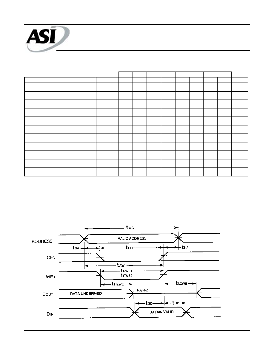
WRITE CYCLE #1
1,2
(CE\ Controlled, OE\ = HIGH or LOW)
NOTES:
1. Test conditions assume signal transition times of 3ns or less, timing reference levels of 1.5V, input pulse levels of 0 to 3.0V and output loading specified in
Figure 1.
2. Tested with the load in Figure 2. Transition is measured ±200 mV from steady-state voltage. Not 100% tested.
3. The internal write time is defined by the overlap of CE\ LOW and WE\ LOW. All signals must be in valid states to initiate a Write, but any one can go
inactive to terminate the Write. The Data Input Setup and Hold timing are referenced to the rising or falling edge of the signal that terminates the Write.
-10
PARAMETER
SYMBOL
MIN
MAX
MIN
MAX
MIN
MAX
MIN
MAX UNITS
Write Cycle Time
t
WC
10
---
12
---
15
---
20
---
ns
CE\ to Write End
t
SCE
7
---
8
---
9
---
10
---
ns
Address Setup Time to Write End
t
AW
8
---
9
---
10
---
12
---
ns
Address Hold from Write End
t
HA
0
---
0
---
0
---
0
---
ns
Address Setup Time
t
SA
0
---
0
---
0
---
0
---
ns
WE\ Pulse Width (OE\ HIGH)
t
PWE1
1
7
---
8
---
9
---
10
---
ns
WE\ Pulse Width (OE\ LOW)
t
PWE2
2
10
---
12
---
12
---
15
---
ns
Data Setup to Write End
t
SD
5
---
6
---
7
---
8
---
ns
Data Hold to Write End
t
HD
0
---
0
---
0
---
0
---
ns
WE\ LOW to High-Z Output
t
HZWE
2
---
5
---
6
---
7
---
8
ns
WE\ HIGH to Low-Z Output
t
LZWE
2
2
---
2
---
2
---
2
---
ns
-20
-12
-15

SRAM
SRAM
SRAM
SRAM
SRAM
AS5LC1008
Austin Semiconductor, Inc.
AS5LC1008
Rev. 1.0 11/02
Austin Semiconductor, Inc. reserves the right to change products or specifications without notice.
7
NOTES:
1. The internal write time is defined by the overlap of CE\ LOW and WE\ LOW. All signals must be in valid states to initiate a Write, but any one can go
inactive to terminate the Write. The Data Input Setup and Hold timing are referenced to the rising or falling edge of the signal that terminates the Write.
2. I/O will assume the High-Z state if OE\ · V
IH
.
WRITE CYCLE #3 (WE\ Controlled, OE\ = LOW during Write Cycle)
WRITE CYCLE #2
1
(WE\ Controlled, OE\ = HIGH during Write Cycle)

SRAM
SRAM
SRAM
SRAM
SRAM
AS5LC1008
Austin Semiconductor, Inc.
AS5LC1008
Rev. 1.0 11/02
Austin Semiconductor, Inc. reserves the right to change products or specifications without notice.
8
ASI Case #906 (Package Designator DJ)
MECHANICAL DEFINITION*
* All measurements are in inches.
MIN
MAX
A
0.128
0.148
A1
0.025
---
A2
0.082
---
B
0.015
0.020
b
0.026
0.032
C
0.007
0.013
D
0.820
0.830
E
0.435
0.445
E1
0.395
0.405
E2
e
0.370 BSC
0.050 BSC
SYMBOL
ASI SPECIFICATIONS

SRAM
SRAM
SRAM
SRAM
SRAM
AS5LC1008
Austin Semiconductor, Inc.
AS5LC1008
Rev. 1.0 11/02
Austin Semiconductor, Inc. reserves the right to change products or specifications without notice.
9
*All measurements are in inches.
ASI Case #501 (Package Designator DCJ)
POSSIBLE FUTURE OFFERING, CONTACT FACTORY
MECHANICAL DEFINITIONS*
A
A2
e
b
D
E
D1
E1
E2
B1
MIN
MAX
A
0.132
0.144
A2
0.026
0.036
B1
0.030
0.040
B1
0.015
0.019
D
0.812
0.828
D1
0.740
0.760
E
0.405
0.415
E1
0.435
0.445
E2
0.360
0.380
e
SYMBOL
ASI SPECIFICATIONS
0.050 BSC

SRAM
SRAM
SRAM
SRAM
SRAM
AS5LC1008
Austin Semiconductor, Inc.
AS5LC1008
Rev. 1.0 11/02
Austin Semiconductor, Inc. reserves the right to change products or specifications without notice.
10
ORDERING INFORMATION
*AVAILABLE PROCESSES
IT = Industrial Temperature Range
-40
o
C to +85
o
C
XT = Military Temperature Range
-55
o
C to +125
o
C
Device Number
Package
Type
Speed
ns
Process
AS5LC1008
DJ
-10
/*
AS5LC1008
DJ
-12
/*
AS5LC1008
DJ
-15
/*
AS5LC1008
DJ
-20
/*
Device Number
Package
Type
Speed
ns
Process
AS5LC1008
DCJ
-10
/*
AS5LC1008
DCJ
-12
/*
AS5LC1008
DCJ
-15
/*
AS5LC1008
DCJ
-20
/*
EXAMPLE: AS5LC1008DJ-12/XT
EXAMPLE: AS5LC1008DCJ-10/IT