UHF POWER TRANSISTOR
DRF1601
The DRF1601 is a low cost, NPN medium power
SiGe HBT(Hetero-Junction Bipolar Transistor)
encapsulated in a plastic SOT-223 SMD package.
The DRF1601 can be used as a driver device or
an output device, depending on the specific app-
lication.
FEATURES
o 6.0 Volt operation
o P1dB 30 dBm @f=900MHz
o Power gain 7 dB @f=900MHz
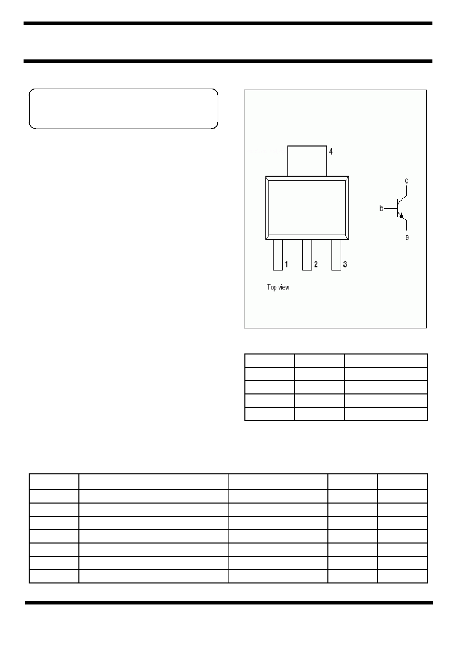
PIN CONFIGURATION
APPLICATIONS
o Hand-held radio equipment in common
emitter class-AB operation in 900 MHz
communication band.
MAXIMUM RATINGS
V
CBO
Collector-Base Voltage
Open Emitter
V
CEO
Collector-Emitter Voltage
Open Base
V
EBO
Emitter-Base Voltage
Open Collector
Ic
Collector Current (DC)
P
T
Total Power Dissipation
Ts = 60 ; note 1
T
STG
Storage Temperature
T
J
Operating Junction Temperature
PIN NO
SYMBOL
DESCRIPTION
SYMBOL
PARAMETER
CONDITION
VALUE
Unit
1
2
3
4
E
B
E
C
30
14
4
450
V
mA
W
emitter
base
collector
emitter
1
-65 ~ 150
150
V
V
NPN SiGe RF TRANSISTOR
www.tachyonics.co.kr
- 1/6 -
Sep-03-2002
2nd Edition
UHF POWER TRANSISTOR
DRF1601
THERMAL CHARACTERISTICS
Rth j-s
PT=1W; Ts=60;note1
* Note 1. Ts is temperature at the soldering point of the collector pin.
QUICK REFERENCE DATA
RF performance at Ts 60 in common emitter test circuit (see Fig 7)
VALUE
Mode of Operation
SYMBOL
PARAMETER
CONDITION
6.0
1000
Unit
thermal resistance from junction
to soldering point
K/W
C
[%]
G
P
[dB]
P
L
[mW]
V
CE
[V]
f [MHz]
7
60
CW, class-AB
900
55
www.tachyonics.co.kr
- 2/6 -
Sep-03-2002
2nd Edition
UHF POWER TRANSISTOR
DRF1601
DC CHARACTERISTICS
Tj=25 unless otherwise specified
BV
CBO
BV
CEO
BV
EBO
I
S
h
FE
C
CB
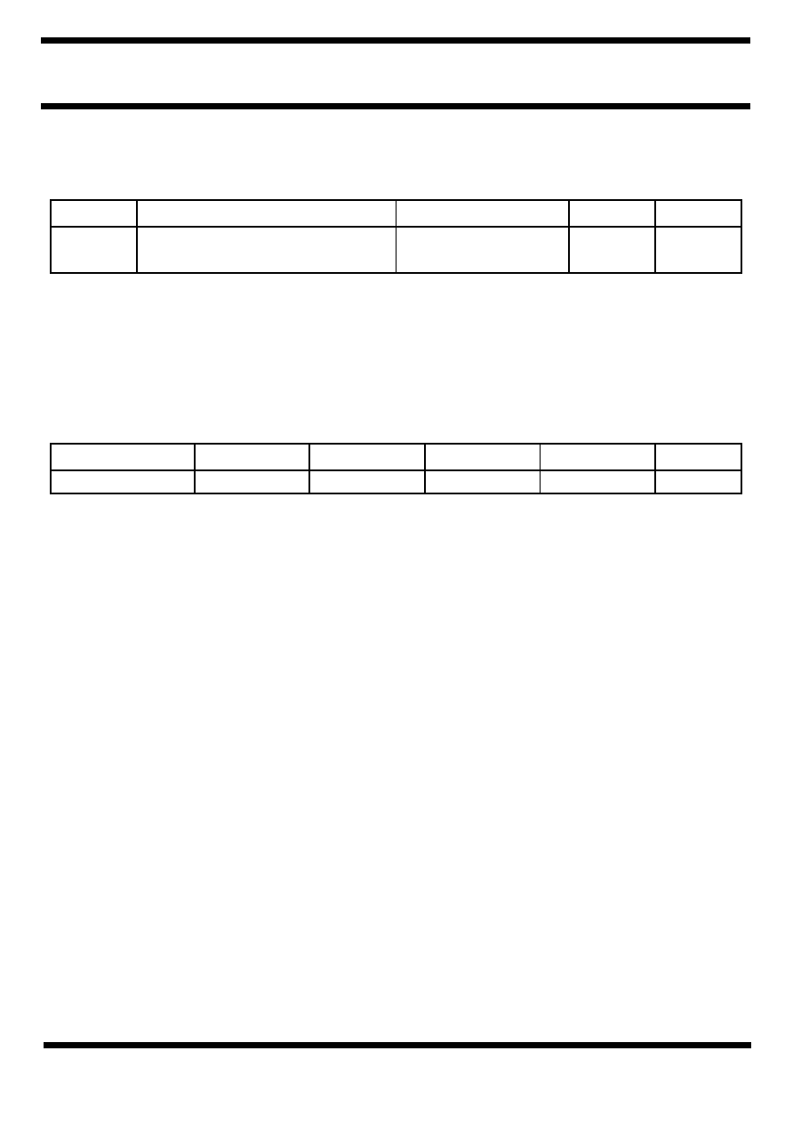
Fig 2. DC Current gain v.s collector current
Fig 3. Collector-base capacitance v.s collector-
base voltage(DC)
SYMBOL
PARAMETER
CONDITION
MIN.
MAX.
UNIT
20
V
14
V
3
V
0.1
mA
60
4.2
pF
DC current gain
collector capacitance
open emitte
open base
open collector
collector-base breakdown voltage
collector-emitter breakdown voltage
emitter-base breakdown voltage
collector leakage current
2
3
4
5
0
2
4
6
8
10
0
20
40
60
80
100
120
140
160
0.00
0.10
0.20
0.30
0.40
Ic(A)
Hfe
V
CE
= 6.0V ; Tj =25
f=900MHz; V
CE
=6.0V; I
CQ
=5mA; Ts < 60
Cc
[pF]
V
CB
[V]
www.tachyonics.co.kr
- 3/6 -
Sep-03-2002
2nd Edition
UHF POWER TRANSISTOR
DRF1601
APPLICATION INFORMATION
RF performance at Ts 60 in common emitter test circuit (see Fig 7)
Mode of Operation
f [MHz]
V
CE
[V]
P
L
[mW]
CW, class-AB
900
6
1000
G
P
[dB]
C
[%]
7
70
Fig 4. Load Power v.s Input power (typical value)
Fig 5. Power gain and collector efficiency v.s load power (typical value)
0
2
4
6
8
10
7.3
14.3
20.9
26.7
30.6
0.0
20.0
40.0
60.0
80.0
100.0
5
10
15
20
25
30
35
0
5
10
15
20
25
30
f=900MHz ; V
CE
=6.0V; I
CQ
=5mA; Ts < 60
P
L
[dBm]
f=900MHz ; I
CQ
=5mA; Ts < 60
G
p
[dB]
C
[%]
P
L
[dBm]
P
L
[dBm]
www.tachyonics.co.kr
- 4/6 -
Sep-03-2002
2nd Edition
UHF POWER TRANSISTOR
DRF1601
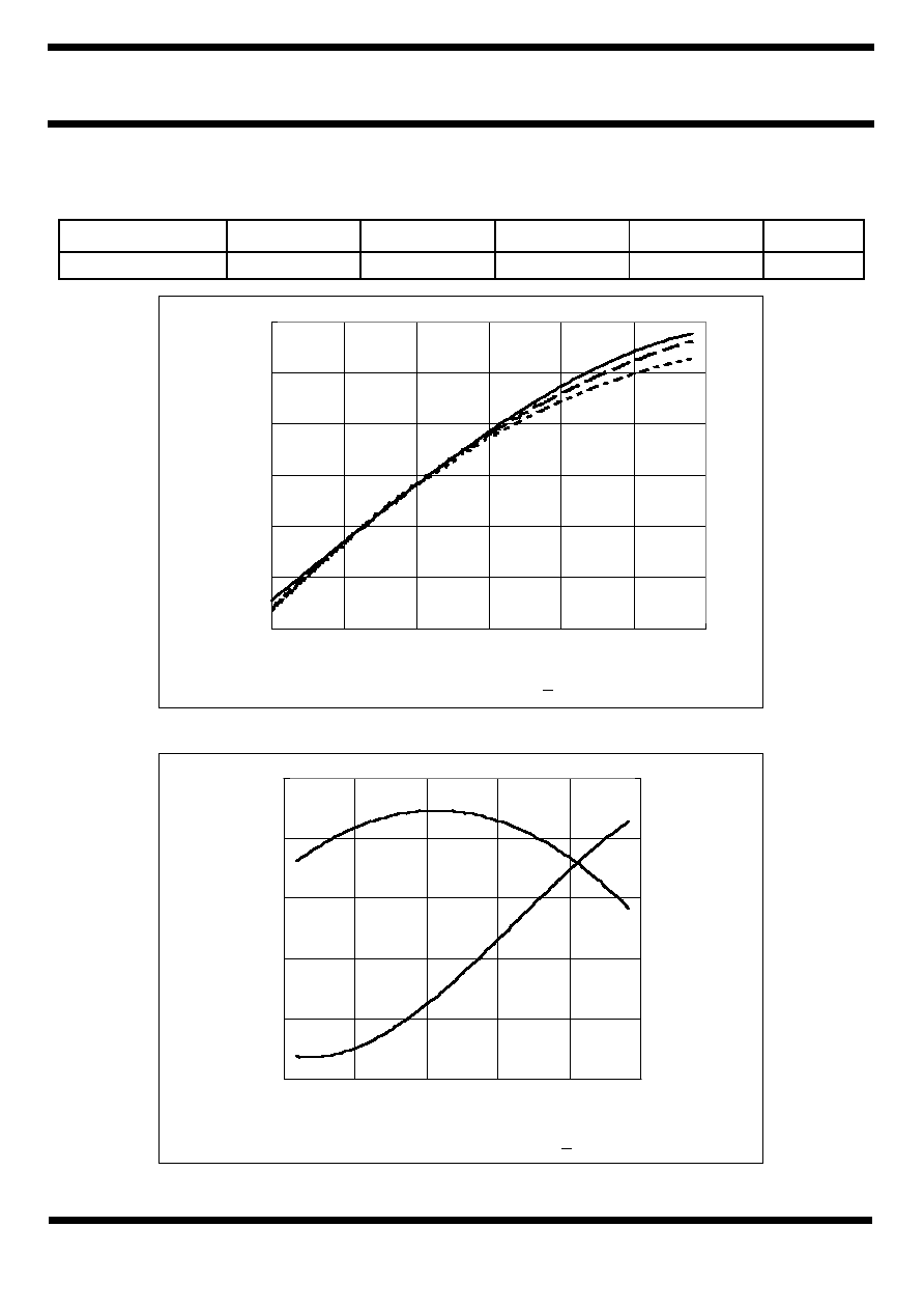
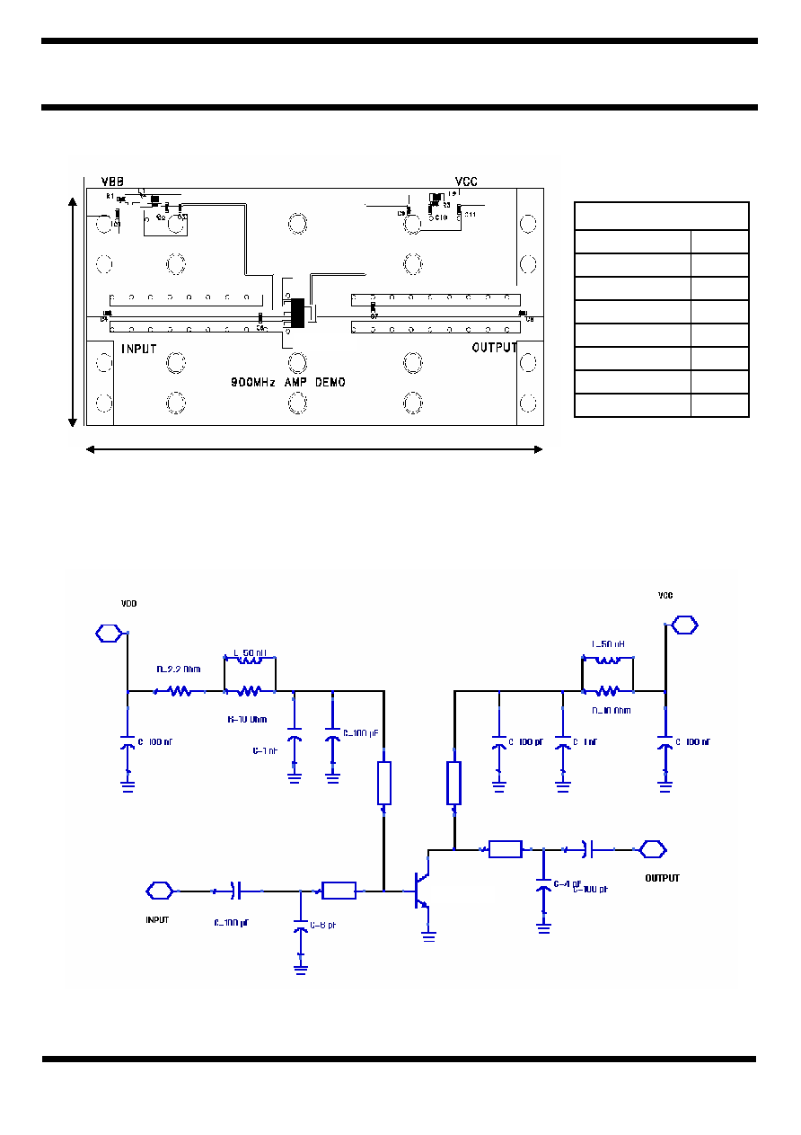
- Test board : FR4 glass epoxy board, dielectric constant = 4.5, thickness = 0.8 mm
- Test condition : CW test, V
CC
= 6.0 V, I
CQ
= 5 mA, frequency = 900 MHz.
100nF
C1, C11
Part List
1nF
100pF
C2, C10
C3, C4, C8, C9
R1
R2, R3
6pF
4pF
C5
C7
Fig 6. Test Circuit Board Layout @ f = 900MHz
Fig 7. Test Circuit Schematic Diagram @f = 900MHz
50nH
L1, L2
2.2
10
53
119
Unit : mm
90, /4 @900 MHz
90, /4 @900 MHz
DRF1601
DRF1601
www.tachyonics.co.kr
- 5/6 -
Sep-03-2002
2nd Edition