U2781B
Rev. A4, 11-Sep-00
1 (10)
Frequency Synthesizer
Description
The programmable frequency synthesizer IC U2781B for
µP-controlled applications is realized with Atmel
Wireless & Microcontrollers' advanced UHF process
which is very suitable for combinations of fast ECL logic
and low-current I
2
L logic. The benefits are high input
sensitivity combined with low power consumption and
therefore small packages (SSO20). This makes the
device a perfect choice for cordless phones and handheld
cellular radio sets up to 1.1 GHz.
Electrostatic sensitive device.
Observe precautions for handling.
Features
D Very low current consumption (typ. 3 V/ 5 mA)
D Supply-voltage range: 2.7 to 5.5 V
D Max. input frequency: 1.1 GHz
D Programmable prescaler 64/ 65 or 128/ 129
D Controlled by 3-wire bus with f
clock
up to 500 kHz
D Status output for PLL lock/ unlock condition
D Very fast phase detector
D SSO20 package
D ESD protection in accordance with MIL-STD. 883
method 3015 class 2
Benefits
D Very low current consumption extends talk time
D Few external components and SSO package save costs
and space
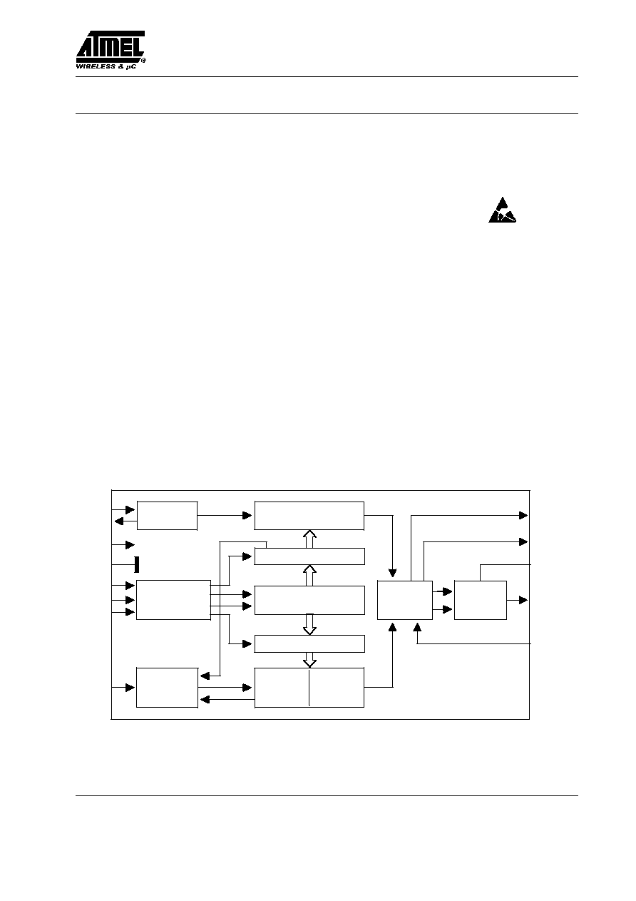
Block Diagram
Charge
pump
Prescaler
64/65
128/129
V
VS
18-bit
shift register
Phase
detector
Oscillator
14-bit
reference counter
Data
Clock
Osci
GND
1-bit latch
load control
PS
CP
LDo
Mo
RFi
Enable
7-bit
swallow
counter
15-bit latch
11-bit
main
18-bit latch
counter
SCP
Osco
17
3
15
1
8
11
7
4
10
6
14
13
5
U2781B
Figure 1. Block diagram
U2781B
Rev. A4, 11-Sep-00
2 (10)
Ordering Information
Extended Type Number
Package
Remarks
U2781B-MFS
SS020
Tube, MOQ 830 pcs
U2781B-MFSG3
SS020
Taped and reeled, MOQ 4000 pcs
Functional Description
The IC is controlled by a 3-wire bus with Clock, Data and
Enable inputs for programming the scaling factors of the
programmable counter, the reference counter and the
prescaler.
A TCXO can be connected to the oscillator input (OSCi)
as an alternative solution to the common crystal reference
oscillator. In that case, the oscillator output (OSCo)
should be left open.
The charge-pump output operates as switched current
sources. The characteristics of the phase-locked loop can
be determinated by the external lowpass filter.
The phase characteristic of the phase detector is convert-
ible and thus matchable to different frequency/ tuning
voltage characteristics.
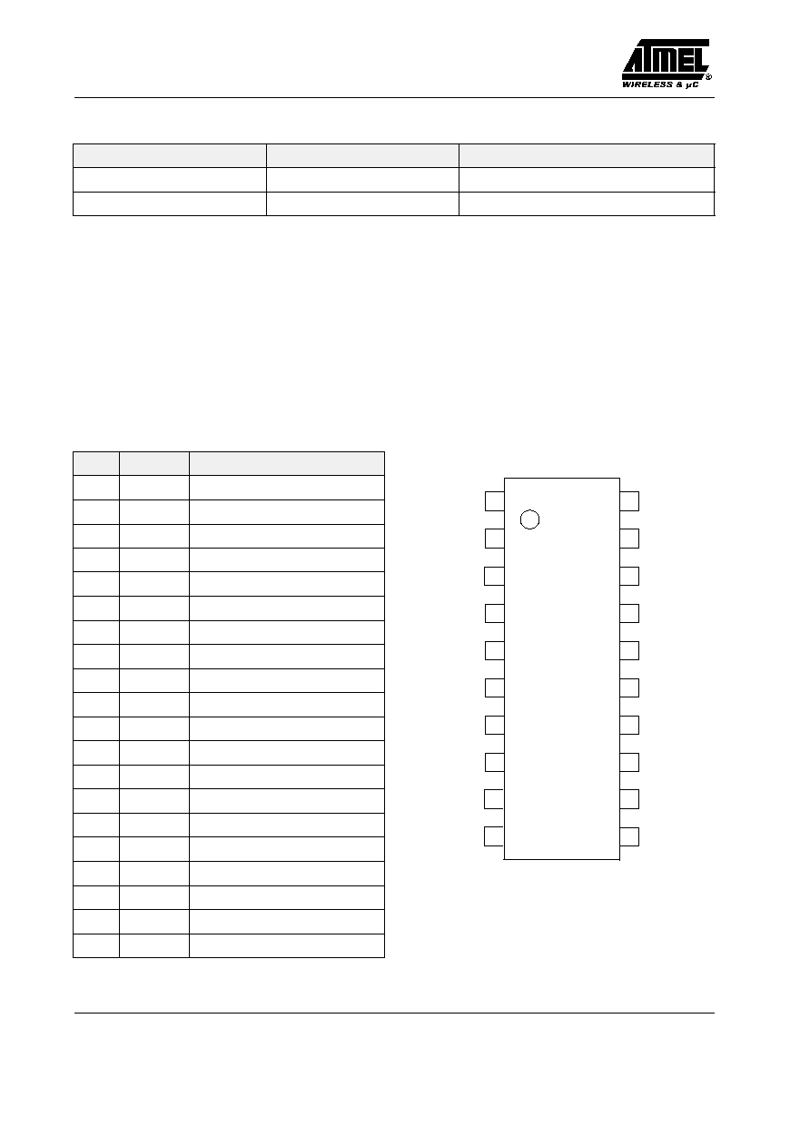
Pin Description
Pin
Symbol
Function
ÁÁÁ
ÁÁÁ
1
ÁÁÁÁÁ
ÁÁÁÁÁ
Osci
ÁÁÁÁÁÁÁÁÁÁ
ÁÁÁÁÁÁÁÁÁÁ
Oscillator input
ÁÁÁ
ÁÁÁ
2
ÁÁÁÁÁ
ÁÁÁÁÁ
n.c.
ÁÁÁÁÁÁÁÁÁÁ
ÁÁÁÁÁÁÁÁÁÁ
Not connected
ÁÁÁ
ÁÁÁ
ÁÁÁ
3
ÁÁÁÁÁ
ÁÁÁÁÁ
ÁÁÁÁÁ
Osco
ÁÁÁÁÁÁÁÁÁÁ
ÁÁÁÁÁÁÁÁÁÁ
ÁÁÁÁÁÁÁÁÁÁ
Oscillator output
ÁÁÁ
ÁÁÁ
4
ÁÁÁÁÁ
ÁÁÁÁÁ
V
SCP
ÁÁÁÁÁÁÁÁÁÁ
ÁÁÁÁÁÁÁÁÁÁ
Charge-pump supply voltage
ÁÁÁ
ÁÁÁ
5
ÁÁÁÁÁ
ÁÁÁÁÁ
V
s
ÁÁÁÁÁÁÁÁÁÁ
ÁÁÁÁÁÁÁÁÁÁ
Supply voltage
ÁÁÁ
ÁÁÁ
6
ÁÁÁÁÁ
ÁÁÁÁÁ
CP
ÁÁÁÁÁÁÁÁÁÁ
ÁÁÁÁÁÁÁÁÁÁ
Charge-pump output
ÁÁÁ
ÁÁÁ
7
ÁÁÁÁÁ
ÁÁÁÁÁ
GND
ÁÁÁÁÁÁÁÁÁÁ
ÁÁÁÁÁÁÁÁÁÁ
Ground
ÁÁÁ
ÁÁÁ
8
ÁÁÁÁÁ
ÁÁÁÁÁ
LDo
ÁÁÁÁÁÁÁÁÁÁ
ÁÁÁÁÁÁÁÁÁÁ
Lock-detector output
ÁÁÁ
ÁÁÁ
ÁÁÁ
9
ÁÁÁÁÁ
ÁÁÁÁÁ
ÁÁÁÁÁ
n.c.
ÁÁÁÁÁÁÁÁÁÁ
ÁÁÁÁÁÁÁÁÁÁ
ÁÁÁÁÁÁÁÁÁÁ
Not connected
ÁÁÁ
ÁÁÁ
10
ÁÁÁÁÁ
ÁÁÁÁÁ
RFi
ÁÁÁÁÁÁÁÁÁÁ
ÁÁÁÁÁÁÁÁÁÁ
VCO input
ÁÁÁ
ÁÁÁ
11
ÁÁÁÁÁ
ÁÁÁÁÁ
Clock
ÁÁÁÁÁÁÁÁÁÁ
ÁÁÁÁÁÁÁÁÁÁ
3-wire bus Clock
ÁÁÁ
ÁÁÁ
12
ÁÁÁÁÁ
ÁÁÁÁÁ
n.c.
ÁÁÁÁÁÁÁÁÁÁ
ÁÁÁÁÁÁÁÁÁÁ
Not connected
ÁÁÁ
ÁÁÁ
13
ÁÁÁÁÁ
ÁÁÁÁÁ
Data
ÁÁÁÁÁÁÁÁÁÁ
ÁÁÁÁÁÁÁÁÁÁ
3-wire bus Data
ÁÁÁ
ÁÁÁ
14
ÁÁÁÁÁ
ÁÁÁÁÁ
Enable
ÁÁÁÁÁÁÁÁÁÁ
ÁÁÁÁÁÁÁÁÁÁ
3-wire bus Enable
ÁÁÁ
ÁÁÁ
15
ÁÁÁÁÁ
ÁÁÁÁÁ
PS
ÁÁÁÁÁÁÁÁÁÁ
ÁÁÁÁÁÁÁÁÁÁ
Phase select input
ÁÁÁ
ÁÁÁ
ÁÁÁ
16
ÁÁÁÁÁ
ÁÁÁÁÁ
ÁÁÁÁÁ
n.c.
ÁÁÁÁÁÁÁÁÁÁ
ÁÁÁÁÁÁÁÁÁÁ
ÁÁÁÁÁÁÁÁÁÁ
Not connected
ÁÁÁ
ÁÁÁ
17
ÁÁÁÁÁ
ÁÁÁÁÁ
Mo
ÁÁÁÁÁÁÁÁÁÁ
ÁÁÁÁÁÁÁÁÁÁ
Monitor output for f
p
and f
r
ÁÁÁ
ÁÁÁ
18
ÁÁÁÁÁ
ÁÁÁÁÁ
n.c.
ÁÁÁÁÁÁÁÁÁÁ
ÁÁÁÁÁÁÁÁÁÁ
Not connected
ÁÁÁ
ÁÁÁ
19
ÁÁÁÁÁ
ÁÁÁÁÁ
n.c.
ÁÁÁÁÁÁÁÁÁÁ
ÁÁÁÁÁÁÁÁÁÁ
Not connected
ÁÁÁ
ÁÁÁ
20
ÁÁÁÁÁ
ÁÁÁÁÁ
n.c.
ÁÁÁÁÁÁÁÁÁÁ
ÁÁÁÁÁÁÁÁÁÁ
Not connected
1
2
3
4
5
6
7
8
10
9
19
18
17
16
14
15
13
12
11
20
V
SCP
V
S
CP
GND
LDo
n.c.
n.c.
Osco
Mo
n.c.
PS
Enable
Data
n.c.
n.c.
n.c.
RFi
Clock
Osci
n.c.
U2781B
Figure 2. Pinning SSO20
U2781B
Rev. A4, 11-Sep-00
3 (10)
Absolute Maximum Ratings
Parameter
Symbol
Value
Unit
ÁÁÁÁÁÁÁÁÁÁÁÁÁÁÁÁÁ
ÁÁÁÁÁÁÁÁÁÁÁÁÁÁÁÁÁ
ÁÁÁÁÁÁÁÁÁÁÁÁÁÁÁÁÁ
Supply voltage
ÁÁÁÁÁ
ÁÁÁÁÁ
ÁÁÁÁÁ
V
S
ÁÁÁÁÁÁÁÁ
ÁÁÁÁÁÁÁÁ
ÁÁÁÁÁÁÁÁ
0.3 to 6
ÁÁÁÁÁ
ÁÁÁÁÁ
ÁÁÁÁÁ
V
ÁÁÁÁÁÁÁÁÁÁÁÁÁÁÁÁÁ
ÁÁÁÁÁÁÁÁÁÁÁÁÁÁÁÁÁ
RF input
ÁÁÁÁÁ
ÁÁÁÁÁ
V
RF
ÁÁÁÁÁÁÁÁ
ÁÁÁÁÁÁÁÁ
V
S
ÁÁÁÁÁ
ÁÁÁÁÁ
V
ÁÁÁÁÁÁÁÁÁÁÁÁÁÁÁÁÁ
ÁÁÁÁÁÁÁÁÁÁÁÁÁÁÁÁÁ
Oscillator input voltage
ÁÁÁÁÁ
ÁÁÁÁÁ
V
Osci
ÁÁÁÁÁÁÁÁ
ÁÁÁÁÁÁÁÁ
1
ÁÁÁÁÁ
ÁÁÁÁÁ
V
ÁÁÁÁÁÁÁÁÁÁÁÁÁÁÁÁÁ
ÁÁÁÁÁÁÁÁÁÁÁÁÁÁÁÁÁ
Oscillator output voltage
ÁÁÁÁÁ
ÁÁÁÁÁ
V
Osco
ÁÁÁÁÁÁÁÁ
ÁÁÁÁÁÁÁÁ
1.5
ÁÁÁÁÁ
ÁÁÁÁÁ
V
ÁÁÁÁÁÁÁÁÁÁÁÁÁÁÁÁÁ
ÁÁÁÁÁÁÁÁÁÁÁÁÁÁÁÁÁ
Bus input voltage
ÁÁÁÁÁ
ÁÁÁÁÁ
V
BUS
ÁÁÁÁÁÁÁÁ
ÁÁÁÁÁÁÁÁ
6
ÁÁÁÁÁ
ÁÁÁÁÁ
V
ÁÁÁÁÁÁÁÁÁÁÁÁÁÁÁÁÁ
ÁÁÁÁÁÁÁÁÁÁÁÁÁÁÁÁÁ
Phase-select input voltage
ÁÁÁÁÁ
ÁÁÁÁÁ
V
PS
ÁÁÁÁÁÁÁÁ
ÁÁÁÁÁÁÁÁ
6
ÁÁÁÁÁ
ÁÁÁÁÁ
V
ÁÁÁÁÁÁÁÁÁÁÁÁÁÁÁÁÁ
ÁÁÁÁÁÁÁÁÁÁÁÁÁÁÁÁÁ
ÁÁÁÁÁÁÁÁÁÁÁÁÁÁÁÁÁ
Charge-pump input voltage
ÁÁÁÁÁ
ÁÁÁÁÁ
ÁÁÁÁÁ
V
SCP
ÁÁÁÁÁÁÁÁ
ÁÁÁÁÁÁÁÁ
ÁÁÁÁÁÁÁÁ
6
ÁÁÁÁÁ
ÁÁÁÁÁ
ÁÁÁÁÁ
V
ÁÁÁÁÁÁÁÁÁÁÁÁÁÁÁÁÁ
ÁÁÁÁÁÁÁÁÁÁÁÁÁÁÁÁÁ
Storage temperature
ÁÁÁÁÁ
ÁÁÁÁÁ
T
stg
ÁÁÁÁÁÁÁÁ
ÁÁÁÁÁÁÁÁ
40 to 125
ÁÁÁÁÁ
ÁÁÁÁÁ
°C
Operating Range
Parameter
Symbol
Value
Unit
Supply voltage
V
S
2.7 to 5.5
V
Ambient temperature
T
amb
40 to 85
°C
Thermal Resistance
Parameter
Symbol
Value
Unit
Junction ambient
SSO20
R
thJA
140
K/W
Electrical Characteristics
T
amb
= 25
_C, V
S
= 2.7 to 5.5 V, unless otherwise specified
Parameter
Test Conditions / Pins
Symbol
Min.
Typ.
Max.
Unit
ÁÁÁÁÁÁÁÁÁÁÁÁÁÁÁÁÁÁÁÁÁÁÁÁÁÁÁÁÁÁÁÁ
ÁÁÁÁÁÁÁÁÁÁÁÁÁÁÁÁÁÁÁÁÁÁÁÁÁÁÁÁÁÁÁÁ
DC supply
ÁÁÁÁÁÁÁÁÁ
ÁÁÁÁÁÁÁÁÁ
Supply voltage
ÁÁÁÁÁÁÁÁÁ
ÁÁÁÁÁÁÁÁÁ
ÁÁÁÁ
ÁÁÁÁ
V
s
ÁÁÁ
ÁÁÁ
2.7
ÁÁÁÁ
ÁÁÁÁ
ÁÁÁÁ
ÁÁÁÁ
5.5
ÁÁÁÁ
ÁÁÁÁ
V
ÁÁÁÁÁÁÁÁÁ
ÁÁÁÁÁÁÁÁÁ
ÁÁÁÁÁÁÁÁÁ
Supply current
ÁÁÁÁÁÁÁÁÁ
ÁÁÁÁÁÁÁÁÁ
ÁÁÁÁÁÁÁÁÁ
V
s
= 3 V
ÁÁÁÁ
ÁÁÁÁ
ÁÁÁÁ
I
s
ÁÁÁ
ÁÁÁ
ÁÁÁ
ÁÁÁÁ
ÁÁÁÁ
ÁÁÁÁ
5
ÁÁÁÁ
ÁÁÁÁ
ÁÁÁÁ
ÁÁÁÁ
ÁÁÁÁ
ÁÁÁÁ
mA
ÁÁÁÁÁÁÁÁÁ
ÁÁÁÁÁÁÁÁÁ
Supply voltage CP
ÁÁÁÁÁÁÁÁÁ
ÁÁÁÁÁÁÁÁÁ
ÁÁÁÁ
ÁÁÁÁ
V
SCP
ÁÁÁ
ÁÁÁ
V
s
ÁÁÁÁ
ÁÁÁÁ
ÁÁÁÁ
ÁÁÁÁ
5.5
ÁÁÁÁ
ÁÁÁÁ
V
ÁÁÁÁÁÁÁÁÁ
ÁÁÁÁÁÁÁÁÁ
ÁÁÁÁÁÁÁÁÁ
Supply current CP
ÁÁÁÁÁÁÁÁÁ
ÁÁÁÁÁÁÁÁÁ
ÁÁÁÁÁÁÁÁÁ
V
CP
= 5 V, PLL in locked
condition
ÁÁÁÁ
ÁÁÁÁ
ÁÁÁÁ
I
SCP
ÁÁÁ
ÁÁÁ
ÁÁÁ
ÁÁÁÁ
ÁÁÁÁ
ÁÁÁÁ
1
ÁÁÁÁ
ÁÁÁÁ
ÁÁÁÁ
ÁÁÁÁ
ÁÁÁÁ
ÁÁÁÁ
µA
ÁÁÁÁÁÁÁÁÁÁÁÁÁÁÁÁÁÁÁÁÁÁÁÁÁÁÁÁÁÁÁÁ
ÁÁÁÁÁÁÁÁÁÁÁÁÁÁÁÁÁÁÁÁÁÁÁÁÁÁÁÁÁÁÁÁ
RF input
ÁÁÁÁÁÁÁÁÁ
ÁÁÁÁÁÁÁÁÁ
ÁÁÁÁÁÁÁÁÁ
Input voltage
f
i
= 200 to 1100 MHz
ÁÁÁÁÁÁÁÁÁ
ÁÁÁÁÁÁÁÁÁ
ÁÁÁÁÁÁÁÁÁ
R
s
= 50
*)
R
s
= 50
*)
ÁÁÁÁ
ÁÁÁÁ
ÁÁÁÁ
V
imin
V
imax
ÁÁÁ
ÁÁÁ
ÁÁÁ
ÁÁÁÁ
ÁÁÁÁ
ÁÁÁÁ
20
200
ÁÁÁÁ
ÁÁÁÁ
ÁÁÁÁ
ÁÁÁÁ
ÁÁÁÁ
ÁÁÁÁ
mV
RMS
mV
RMS
ÁÁÁÁÁÁÁÁÁ
ÁÁÁÁÁÁÁÁÁ
Frequency range
ÁÁÁÁÁÁÁÁÁ
ÁÁÁÁÁÁÁÁÁ
ÁÁÁÁ
ÁÁÁÁ
f
imin
f
imax
ÁÁÁ
ÁÁÁ
1100
ÁÁÁÁ
ÁÁÁÁ
50
1250
ÁÁÁÁ
ÁÁÁÁ
ÁÁÁÁ
ÁÁÁÁ
MHz
MHz
ÁÁÁÁÁÁÁÁÁ
ÁÁÁÁÁÁÁÁÁ
ÁÁÁÁÁÁÁÁÁ
Scaling factor prescaler
ÁÁÁÁÁÁÁÁÁ
ÁÁÁÁÁÁÁÁÁ
ÁÁÁÁÁÁÁÁÁ
ÁÁÁÁ
ÁÁÁÁ
ÁÁÁÁ
S
PSC
ÁÁÁ
ÁÁÁ
ÁÁÁ
ÁÁÁÁ
ÁÁÁÁ
ÁÁÁÁ
64/128
ÁÁÁÁ
ÁÁÁÁ
ÁÁÁÁ
ÁÁÁÁ
ÁÁÁÁ
ÁÁÁÁ
ÁÁÁÁÁÁÁÁÁ
ÁÁÁÁÁÁÁÁÁ
Scaling factors main counter
ÁÁÁÁÁÁÁÁÁ
ÁÁÁÁÁÁÁÁÁ
ÁÁÁÁ
ÁÁÁÁ
S
M
ÁÁÁ
ÁÁÁ
4
ÁÁÁÁ
ÁÁÁÁ
ÁÁÁÁ
ÁÁÁÁ
2047
ÁÁÁÁ
ÁÁÁÁ

U2781B
Rev. A4, 11-Sep-00
4 (10)
Electrical Characteristics (continued)
T
amb
= 25
_C, V
S
= 2.7 to 5.5 V, unless otherwise specified
Unit
Max.
Typ.
Min.
Symbol
Test Conditions / Pins
Parameter
ÁÁÁÁÁÁÁÁÁ
ÁÁÁÁÁÁÁÁÁ
Scaling factors swallow
counter
ÁÁÁÁÁÁÁÁÁÁ
ÁÁÁÁÁÁÁÁÁÁ
ÁÁÁÁ
ÁÁÁÁ
S
S
ÁÁÁ
ÁÁÁ
0
ÁÁÁÁ
ÁÁÁÁ
ÁÁÁÁ
ÁÁÁÁ
127
ÁÁÁÁ
ÁÁÁÁ
ÁÁÁÁÁÁÁÁÁÁÁÁÁÁÁÁÁÁÁÁÁÁÁÁÁÁÁÁÁÁÁÁ
ÁÁÁÁÁÁÁÁÁÁÁÁÁÁÁÁÁÁÁÁÁÁÁÁÁÁÁÁÁÁÁÁ
ÁÁÁÁÁÁÁÁÁÁÁÁÁÁÁÁÁÁÁÁÁÁÁÁÁÁÁÁÁÁÁÁ
Reference oscillator
ÁÁÁÁÁÁÁÁÁ
ÁÁÁÁÁÁÁÁÁ
Input voltage
ÁÁÁÁÁÁÁÁÁÁ
ÁÁÁÁÁÁÁÁÁÁ
R
s
= 50
*)
R
s
= 50
*)
ÁÁÁÁ
ÁÁÁÁ
V
imin
V
imax
ÁÁÁ
ÁÁÁ
ÁÁÁÁ
ÁÁÁÁ
20
200
ÁÁÁÁ
ÁÁÁÁ
ÁÁÁÁ
ÁÁÁÁ
mV
RMS
mV
RMS
ÁÁÁÁÁÁÁÁÁ
ÁÁÁÁÁÁÁÁÁ
ÁÁÁÁÁÁÁÁÁ
Frequency range
ÁÁÁÁÁÁÁÁÁÁ
ÁÁÁÁÁÁÁÁÁÁ
ÁÁÁÁÁÁÁÁÁÁ
ÁÁÁÁ
ÁÁÁÁ
ÁÁÁÁ
f
imin
f
imax
ÁÁÁ
ÁÁÁ
ÁÁÁ
ÁÁÁÁ
ÁÁÁÁ
ÁÁÁÁ
0,1
20
ÁÁÁÁ
ÁÁÁÁ
ÁÁÁÁ
ÁÁÁÁ
ÁÁÁÁ
ÁÁÁÁ
MHz
MHz
ÁÁÁÁÁÁÁÁÁ
ÁÁÁÁÁÁÁÁÁ
ÁÁÁÁÁÁÁÁÁ
Scaling factor reference
counter
ÁÁÁÁÁÁÁÁÁÁ
ÁÁÁÁÁÁÁÁÁÁ
ÁÁÁÁÁÁÁÁÁÁ
ÁÁÁÁ
ÁÁÁÁ
ÁÁÁÁ
S
R
ÁÁÁ
ÁÁÁ
ÁÁÁ
4
ÁÁÁÁ
ÁÁÁÁ
ÁÁÁÁ
ÁÁÁÁ
ÁÁÁÁ
ÁÁÁÁ
16383
ÁÁÁÁ
ÁÁÁÁ
ÁÁÁÁ
ÁÁÁÁÁÁÁÁÁÁÁÁÁÁÁÁÁÁÁÁÁÁÁÁÁÁÁÁÁÁÁÁ
ÁÁÁÁÁÁÁÁÁÁÁÁÁÁÁÁÁÁÁÁÁÁÁÁÁÁÁÁÁÁÁÁ
3-wire bus (Clock, Data, Enable) and PS
ÁÁÁÁÁÁÁÁÁ
ÁÁÁÁÁÁÁÁÁ
High input voltage
ÁÁÁÁÁÁÁÁÁÁ
ÁÁÁÁÁÁÁÁÁÁ
ÁÁÁÁ
ÁÁÁÁ
V
iH
ÁÁÁ
ÁÁÁ
1.5
ÁÁÁÁ
ÁÁÁÁ
0.9
ÁÁÁÁ
ÁÁÁÁ
ÁÁÁÁ
ÁÁÁÁ
V
ÁÁÁÁÁÁÁÁÁ
ÁÁÁÁÁÁÁÁÁ
Low input voltage
ÁÁÁÁÁÁÁÁÁÁ
ÁÁÁÁÁÁÁÁÁÁ
ÁÁÁÁ
ÁÁÁÁ
V
iL
ÁÁÁ
ÁÁÁ
0
ÁÁÁÁ
ÁÁÁÁ
ÁÁÁÁ
ÁÁÁÁ
0.4
ÁÁÁÁ
ÁÁÁÁ
V
ÁÁÁÁÁÁÁÁÁ
ÁÁÁÁÁÁÁÁÁ
ÁÁÁÁÁÁÁÁÁ
High input current
ÁÁÁÁÁÁÁÁÁÁ
ÁÁÁÁÁÁÁÁÁÁ
ÁÁÁÁÁÁÁÁÁÁ
ÁÁÁÁ
ÁÁÁÁ
ÁÁÁÁ
I
iH
ÁÁÁ
ÁÁÁ
ÁÁÁ
ÁÁÁÁ
ÁÁÁÁ
ÁÁÁÁ
ÁÁÁÁ
ÁÁÁÁ
ÁÁÁÁ
5
ÁÁÁÁ
ÁÁÁÁ
ÁÁÁÁ
µA
ÁÁÁÁÁÁÁÁÁ
ÁÁÁÁÁÁÁÁÁ
Low input current
ÁÁÁÁÁÁÁÁÁÁ
ÁÁÁÁÁÁÁÁÁÁ
ÁÁÁÁ
ÁÁÁÁ
I
iL
ÁÁÁ
ÁÁÁ
5
ÁÁÁÁ
ÁÁÁÁ
ÁÁÁÁ
ÁÁÁÁ
ÁÁÁÁ
ÁÁÁÁ
µA
ÁÁÁÁÁÁÁÁÁÁÁÁÁÁÁÁÁÁÁÁÁÁÁÁÁÁÁÁÁÁÁÁ
ÁÁÁÁÁÁÁÁÁÁÁÁÁÁÁÁÁÁÁÁÁÁÁÁÁÁÁÁÁÁÁÁ
Monitor output (Emitter follower)
ÁÁÁÁÁÁÁÁÁ
ÁÁÁÁÁÁÁÁÁ
High output voltage
ÁÁÁÁÁÁÁÁÁÁ
ÁÁÁÁÁÁÁÁÁÁ
V
s
= 3 V
ÁÁÁÁ
ÁÁÁÁ
V
iH
ÁÁÁ
ÁÁÁ
2.1
ÁÁÁÁ
ÁÁÁÁ
2.2
ÁÁÁÁ
ÁÁÁÁ
ÁÁÁÁ
ÁÁÁÁ
V
ÁÁÁÁÁÁÁÁÁ
ÁÁÁÁÁÁÁÁÁ
Low output voltage
ÁÁÁÁÁÁÁÁÁÁ
ÁÁÁÁÁÁÁÁÁÁ
I
MO
= 0.5 mA
ÁÁÁÁ
ÁÁÁÁ
V
iL
ÁÁÁ
ÁÁÁ
ÁÁÁÁ
ÁÁÁÁ
1.8
ÁÁÁÁ
ÁÁÁÁ
1.9
ÁÁÁÁ
ÁÁÁÁ
V
ÁÁÁÁÁÁÁÁÁ
ÁÁÁÁÁÁÁÁÁ
Charge-pump output
ÁÁÁÁÁÁÁÁÁÁ
ÁÁÁÁÁÁÁÁÁÁ
ÁÁÁÁ
ÁÁÁÁ
ÁÁÁ
ÁÁÁ
ÁÁÁÁ
ÁÁÁÁ
ÁÁÁÁ
ÁÁÁÁ
ÁÁÁÁ
ÁÁÁÁ
ÁÁÁÁÁÁÁÁÁ
ÁÁÁÁÁÁÁÁÁ
ÁÁÁÁÁÁÁÁÁ
Source current
ÁÁÁÁÁÁÁÁÁÁ
ÁÁÁÁÁÁÁÁÁÁ
ÁÁÁÁÁÁÁÁÁÁ
V
CP
= 5 V
ÁÁÁÁ
ÁÁÁÁ
ÁÁÁÁ
I
source
ÁÁÁ
ÁÁÁ
ÁÁÁ
ÁÁÁÁ
ÁÁÁÁ
ÁÁÁÁ
1
ÁÁÁÁ
ÁÁÁÁ
ÁÁÁÁ
ÁÁÁÁ
ÁÁÁÁ
ÁÁÁÁ
mA
ÁÁÁÁÁÁÁÁÁ
ÁÁÁÁÁÁÁÁÁ
Sink current
ÁÁÁÁÁÁÁÁÁÁ
ÁÁÁÁÁÁÁÁÁÁ
ÁÁÁÁ
ÁÁÁÁ
I
sink
ÁÁÁ
ÁÁÁ
ÁÁÁÁ
ÁÁÁÁ
1
ÁÁÁÁ
ÁÁÁÁ
ÁÁÁÁ
ÁÁÁÁ
mA
ÁÁÁÁÁÁÁÁÁ
ÁÁÁÁÁÁÁÁÁ
Leakage current
ÁÁÁÁÁÁÁÁÁÁ
ÁÁÁÁÁÁÁÁÁÁ
V
CP
= 5 V
ÁÁÁÁ
ÁÁÁÁ
I
leak
ÁÁÁ
ÁÁÁ
ÁÁÁÁ
ÁÁÁÁ
±5
ÁÁÁÁ
ÁÁÁÁ
ÁÁÁÁ
ÁÁÁÁ
nA
ÁÁÁÁÁÁÁÁÁÁÁÁÁÁÁÁÁÁÁÁÁÁÁÁÁÁÁÁÁÁÁÁ
ÁÁÁÁÁÁÁÁÁÁÁÁÁÁÁÁÁÁÁÁÁÁÁÁÁÁÁÁÁÁÁÁ
Lock-detector output (open collector)
ÁÁÁÁÁÁÁÁÁ
ÁÁÁÁÁÁÁÁÁ
Saturation voltage
ÁÁÁÁÁÁÁÁÁÁ
ÁÁÁÁÁÁÁÁÁÁ
I
LD
= 0.2 mA
ÁÁÁÁ
ÁÁÁÁ
V
sat
ÁÁÁ
ÁÁÁ
ÁÁÁÁ
ÁÁÁÁ
0.2
ÁÁÁÁ
ÁÁÁÁ
0.4
ÁÁÁÁ
ÁÁÁÁ
V
ÁÁÁÁÁÁÁÁÁ
ÁÁÁÁÁÁÁÁÁ
Leakage current
ÁÁÁÁÁÁÁÁÁÁ
ÁÁÁÁÁÁÁÁÁÁ
V
LD
= 5 V
ÁÁÁÁ
ÁÁÁÁ
I
leak
ÁÁÁ
ÁÁÁ
ÁÁÁÁ
ÁÁÁÁ
ÁÁÁÁ
ÁÁÁÁ
2
ÁÁÁÁ
ÁÁÁÁ
mA
*) RMS voltage at 50
W

U2781B
Rev. A4, 11-Sep-00
5 (10)
Functional Description
The reference- and the programmable counter can be
programmed by the 3-wire bus (Clock, Data and Enable).
The Data Signal is transferred bit by bit into the shift
register during the rising edge, starting with the MSB-bit.
As soon as the enable signal is in high condition, the
content of the shift register will be taken over either into
the 15-bit reference counter latch (C = H) or into the
18-bit latch of the programmable counter (C = L)
Reference Counter (15-bit shift register)
ÁÁÁ
ÁÁÁ
LSB
ÁÁÁ
ÁÁÁ
ÁÁÁ
ÁÁÁ
ÁÁÁ
ÁÁÁ
ÁÁÁ
ÁÁÁ
ÁÁ
ÁÁ
ÁÁÁ
ÁÁÁ
ÁÁÁ
ÁÁÁ
ÁÁÁ
ÁÁÁ
ÁÁÁ
ÁÁÁ
ÁÁÁ
ÁÁÁ
ÁÁÁ
ÁÁÁ
ÁÁÁ
ÁÁÁ
ÁÁÁ
ÁÁÁ
ÁÁÁ
ÁÁÁ
ÁÁÁ
ÁÁÁ
MSB
ÁÁÁ
ÁÁÁ
C
ÁÁÁ
ÁÁÁ
R0
ÁÁÁ
ÁÁÁ
R1
ÁÁÁ
ÁÁÁ
R2
ÁÁÁ
ÁÁÁ
R3
ÁÁ
ÁÁ
R4
ÁÁÁ
ÁÁÁ
R5
ÁÁÁ
ÁÁÁ
R6
ÁÁÁ
ÁÁÁ
R7
ÁÁÁ
ÁÁÁ
R8
ÁÁÁ
ÁÁÁ
R9
ÁÁÁ
ÁÁÁ
R10
ÁÁÁ
ÁÁÁ
R11
ÁÁÁ
ÁÁÁ
R12
ÁÁÁ
ÁÁÁ
R13
ÁÁÁ
ÁÁÁ
PSC
C:
Control bit High
PSC: Prescaler scaling factor bit: High 64/65
Low 128/129
S
PSC
= 64 or 128
R0 to R13:
These bits are setting the reference counter S
R
S
R
= R0
2
0
+ R1
2
1
+ to + R12
2
12
+ R13
2
13
permitted scaling factors for S
R
: 4 to 16383
Programmable Counter (18-bit shift register)
ÁÁÁ
ÁÁÁ
LSB
ÁÁÁ
ÁÁÁ
ÁÁ
ÁÁ
ÁÁÁ
ÁÁÁ
ÁÁ
ÁÁ
ÁÁÁ
ÁÁÁ
ÁÁÁ
ÁÁÁ
ÁÁ
ÁÁ
ÁÁÁ
ÁÁÁ
ÁÁ
ÁÁ
ÁÁÁ
ÁÁÁ
ÁÁ
ÁÁ
ÁÁÁ
ÁÁÁ
ÁÁ
ÁÁ
ÁÁÁ
ÁÁÁ
ÁÁ
ÁÁ
ÁÁÁ
ÁÁÁ
ÁÁÁ
ÁÁÁ
ÁÁÁ
ÁÁÁ
MSB
ÁÁÁ
ÁÁÁ
C
ÁÁÁ
ÁÁÁ
S0
ÁÁ
ÁÁ
S1
ÁÁÁ
ÁÁÁ
S2
ÁÁ
ÁÁ
S3
ÁÁÁ
ÁÁÁ
S4
ÁÁÁ
ÁÁÁ
S5
ÁÁ
ÁÁ
S6
ÁÁÁ
ÁÁÁ
M0
ÁÁ
ÁÁ
M1
ÁÁÁ
ÁÁÁ
M2
ÁÁ
ÁÁ
M3
ÁÁÁ
ÁÁÁ
M4
ÁÁ
ÁÁ
M5
ÁÁÁ
ÁÁÁ
M6
ÁÁ
ÁÁ
M7
ÁÁÁ
ÁÁÁ
M8
ÁÁÁ
ÁÁÁ
M9
ÁÁÁ
ÁÁÁ
M10
C:
Control bit Low
S0 to S6:
These bits are setting the swallow counter S
S
.
S
S
= S0
2
0
+ S1
2
1
+ to + S5
2
5
+ S6
2
6
permitted scaling factors for S
S
: 0 to 127, S
S
< S
M
M0 to M10 : These bits are setting the main counter S
M
.
S
M
= M0
2
0
+ M1
2
1
+ to + M9
2
9
+ M10
2
10
permitted scaling factors for S
M
: 4 to 2047
Total scaling factor S
P
of the programmable counter
S
P
= (S
PSC
S
M
) + S
S
Condition: S
S
< S
M
VCO Frequency
f
VCO
= ((S
PSC
S
M
) + S
S
)
f
RefOsc
/ S
R