2101D�BDC�06/04
Features
�
Up to 2 Gsps Sampling Rate
�
Power Consumption: 4.6 W
�
500 mVpp Differential 100
or Single-ended 50 (�2 %) Analog Inputs
�
Differential 100
or Single-ended 50 Clock Inputs
�
ECL or LVDS Output Compatibility
�
50
Differential Outputs with Common Mode not Dependent on Temperature
�
ADC Gain Adjust
�
Sampling Delay Adjust
�
Offset Control Capability
�
Data Ready Output with Asynchronous Reset
�
Out-of-range Output Bit
�
Selectable Decimation by 32 Functions
�
Gray or Binary Selectable Output Data; NRZ Output Mode
�
Pattern Generator Output (for Acquisition System Monitoring)
�
Radiation Tolerance Oriented Design (More Than 100 Krad (Si) Expected)
�
CBGA 152 Cavity Down Hermetic Package
�
CBGA Package Evaluation Board TSEV83102G0BGL
�
Companion Device: DMUX 8-/10-bit 1:4/1:8 2 Gsps TS81102G0
Performance
�
3.3 GHz Full Power Input Bandwidth (-3 dB)
�
Gain Flatness: � 0.2 dB (from DC up to 1.5 GHz)
�
Low Input VSWR: 1.2 Max from DC to 2.5 GHz
�
SFDR = -59 dBc; 7.6 Effective Bits at F
S
= 1.4 Gsps, F
IN
= 700 MHz [-1 dBFS]
�
SFDR = -53 dBc; 7.1 Effective Bits at Fs = 1.4 Gsps, F
IN
= 1950 MHz [-1 dBFS]
�
SFDR = -54 dBc; 6.5 Effective Bits at F
S
= 2 Gsps, F
IN
= 2 GHz [-1 dBFS]
�
Low Bit Error Rate (10
-12
) at 2 Gsps
Application
�
Direct RF Down Conversion
�
Wide Band Satellite Receiver
�
High-speed Instrumentation
�
High-speed Acquisition Systems
�
High-energy Physics
�
Automatic Test Equipment
�
Radar
Screening
�
Temperature Range for Packaged Device:
�
"C" grade: 0
� C < Tc; Tj < 90� C
�
"V" grade: -20
� C < Tc; Tj < 110� C
�
Standard Die Flow (upon Request)
Description
The TS83102G0B is a monolithic 10-bit analog-to-digital converter, designed for digi-
tizing wide bandwidth analog signals at very high sampling rates of up to 2 Gsps. It
uses an innovative architecture, including an on-chip Sample and Hold (S/H). The
3.3 GHz full power input bandwidth and band flatness performances enable the digitiz-
ing of high IF and large bandwidth signals.
10-bit 2 Gsps
ADC
TS83102G0B

2
TS83102G0B
2101D�BDC�06/04
Figure 1. Simplified Block Diagram
Functional Description
The TS83102G0B is a 10-bit 2 Gsps ADC. The device includes a front-end master/slave Track
and Hold stage (Sample and Hold), followed by an analog encoding stage (Analog Quantizer),
which outputs analog residues resulting from analog quantization. Successive banks of
latches regenerate the analog residues into logical levels before entering an error correction
circuit and resynchronization stage, followed by 50
differential output buffers.
The TS83102G0B works in a fully differential mode from analog inputs to digital outputs. A dif-
ferential Data Ready output (DR/DRB) is available to indicate when the outputs are valid and
an Asynchronous Data Ready Reset ensures that the first digitized data corresponds to the
first acquisition.
The control pin B/GB (A11 of the CBGA package) is provided to select either a binary or gray
data output format. The gain control pin GA (R9 of the CBGA package) is provided to adjust
the ADC gain transfer function.
A Sampling Delay Adjust function (SDA) may be used to ease the interleaving of ADCs.
A pattern generator is integrated on the chip for debug or acquisition setup. This function is
activated through the PGEB pin (A9 of the CBGA package).
An Out-of-range bit (OR/ORB) indicates when the input overrides 0.5 Vpp.
A selectable decimation by 32 functions is also available for enhanced testability coverage
(A10 of the CBGA package), along with the die junction temperature monitoring function.
The TS83102G0B uses only vertical isolated NPN transistors together with oxide isolated pol-
ysilicon resistors, which allows enhanced radiation tolerance (over 100 kRad (Si) total dose
expected tolerance).
Sample &Hold
Clock generation
Logic block
Analog
Q
uant
izer
VIN
VINB
CLK
CLKB
PGEB B/GB
DRRB
OR
ORB
D9
D9B
D0
D0B
GA
DR
DRB
50
50
50
50
SDA
SDA
DECB/
DIODE
3
TS83102G0B
2101D�BDC�06/04
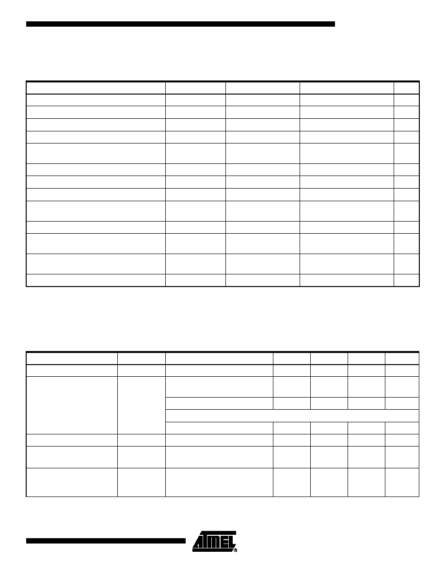
Specification
Note:
Absolute maximum ratings are short term limiting values (referenced to GND = 0V), to be applied individually, while other
parameters are within specified operating conditions. Long exposure to maximum ratings may affect device reliability. All inte-
grated circuits have to be handled with appropriate care to avoid damage due to ESD. Damage caused by inappropriate
handling or storage could range from performance degradation to complete failure.
Absolute Maximum Ratings
Parameter
Symbol
Comments
Value
Unit
Positive supply voltage
V
CC
GND to 6.0
V
Digital negative supply voltage
D
VEE
GND to -5.7
V
Digital positive supply voltage
V
PLUSD
GND - 1.1 to 2.5
V
Negative supply voltage
V
EE
GND to -5.5
V
Maximum difference between negative
supply voltages
D
VEE
to V
EE
0.3
V
Analog input voltages
V
IN
or V
INB
-1.5 to 1.5
V
Maximum difference between VIN and VINB
V
IN
- V
INB
-1.5 to 1.5
V
Clock input voltage
V
CLK
or V
CLKB
-1 to 1
V
Maximum difference between VCLK and
VCLKB
V
CLK
- V
CLKB
-1 to 1
Vpp
Static input voltage
V
D
GA, SDA
-5 to 0.8
V
Digital input voltage
V
D
SDAEN, DRRB, B/GB,
PGEB, DECB
-5 to 0.8
V
Digital output voltage
V
O
V
PLUSD
min operating -2.2 to
V
PLUSD
max operating + 0.8
V
Junction temperature
T
J
130
�C
Recommended Conditions of Use
Parameter
Symbol
Comments
Min
Typ
Max
Unit
Positive supply voltage
V
CC
4.75
5
5.25
V
Positive digital supply
voltage
V
PLUSD
Differential ECL output
compatibility
- 0.9
- 0.8
- 0.7
V
LVDS output compatibility
1.375
1.45
1.525
V
Grounded
(1)
Maximum operating VPLUSD
1.7
V
Negative supply voltages
V
EE
, D
VEE
- 5.25
- 5.0
- 4.75
V
Differential analog input
voltage (full-scale)
V
IN
, V
INB
V
IN
- V
INB
50
differential or single-ended
�113
450
�125
500
�137
550
mV
mVpp
Clock input power level
(ground common mode)
P
CLK
, P
CLKB
50
single-ended clock input or
100
differential clock
(recommended)
- 4
0
4
dBm
4
TS83102G0B
2101D�BDC�06/04
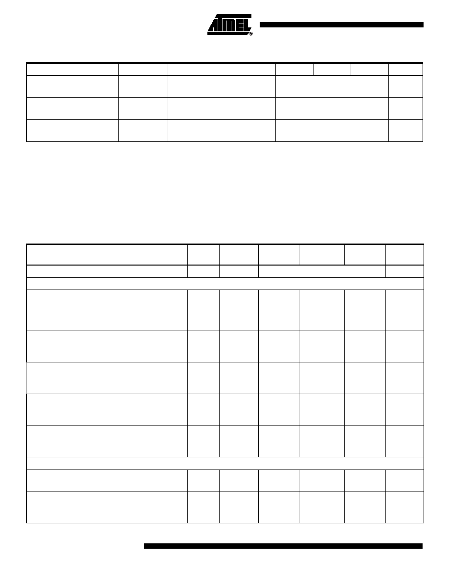
Note:
1.
ADC performances are independent on V
PLUSD
common mode voltage and performances are guaranteed in the
limits of the specified V
PLUSD
range (from -0.9V to 1.7V).
Operating Temperature
Range
Commercial "C" grade
Industrial "V" grade
0�C < T
C
; T
J
< 90�C
-20�C < T
C
; T
J
< 110�C
�C
Storage Temperature
Tstg
-65 to 150
�C
Lead Temperature
Tlead
300
�C
Electrical Operating Characteristics
V
CC
= 5V ; V
PLUSD
= 0V (unless otherwise specified). ADC performances are independent of V
PLUSD
common mode
voltage and performances are guaranteed within the limits of the specified V
PLUSD
range (from -0.9V to 1.7V);
V
EE
= D
VEE
= -5V; V
IN
- V
INB
= 500 mVpp (full-scale single-ended or differential input);
clock inputs differential driven; analog-input single-ended driven.
Parameter
Test
Level
Symbol
Min
Typ
Max
Unit
Resolution
10
Bits
Power Requirements
Positive supply voltage
- analog
- digital (ECL)
- digital (LVDS)
1
1
4
V
CC
V
PLUSD
V
PLUSD
4.75
5
- 0.8
1.45
5.25
V
V
V
Positive supply current
- analog
- digital
1
1
I
VCC
I
VPLUSD
138
154
205
200
mA
mA
Negative supply voltage
- analog
- digital
1
1
V
EE
D
VEE
-5.25
-5.25
-5
-5
-4.75
-4.75
V
V
Negative supply current
- analog
- digital
1
1
V
EE
I
DVEE
615
160
750
200
mA
mA
Power dissipation
- ECL
- LVDS
1
4
P
D
4.6
5.0
5.2
5.7
W
W
Analog Inputs
Full-scale input voltage range (differential mode)
(0 V common mode voltage)
4
4
V
IN,
V
INB
- 125
- 125
125
125
mV
mV
Full-scale input voltage range (single-ended input
option)
(0 V common mode voltage)
4
4
V
IN,
V
INB
- 250
0
250
mV
mV
Recommended Conditions of Use (Continued)
Parameter
Symbol
Comments
Min
Typ
Max
Unit
5
TS83102G0B
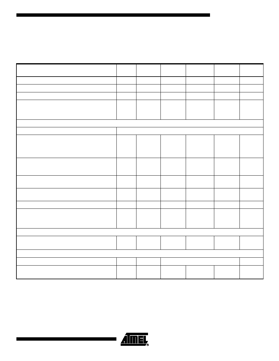
2101D�BDC�06/04
Analog input power level (50
single-ended)
4
P
IN
- 2
dBm
Analog input capacitance (die)
4
C
IN
0.3
pF
Input leakage current
4
I
IN
10
�A
Input resistance
- single-ended
- differential
4
4
R
IN
R
IN
49
98
50
100
51
102
Clock Inputs
Logic common mode compatibility for clock inputs
Differential ECL to LVDS
Clock inputs common voltage range (V
CLK
or V
CLKB
)
(DC coupled clock input)
AC coupled for LVDS compatibility (common mode
1.2V)
4
V
CM
-1.2
0
0.3
V
Clock input power level (low-phase noise sinewave
input)
50
single-ended or 100 differential
4
P
CLK
-4
0
4
dBm
Clock input swing (single ended; with CLKB = 50
to GND)
4
V
CLK
�200
�320
�500
mV
Clock input swing (differential voltage) - on each
clock input
4
V
CLK
V
CLKB
�141
�226
�354
mV
Clock input capacitance (die)
4
C
CLK
0.3
pF
Clock input resistance
- single-ended
- differential ended
R
CLK
R
CLK
45
90
50
100
55
110
Digital Inputs (SDAEN, PGEB, DECB/Diode, B/GB, DRRB)
- logic low
- logic high
4
V
IL
V
IH
-5
-2
-3
0
V
V
Digital Inputs (DRRB Only)
Logic Compatibility
Negative ECL
- logic low
- logic high
4
V
IL
V
IH
-1.810
-1.165
-1.625
-0.880
V
V
Electrical Operating Characteristics (Continued)
V
CC
= 5V ; V
PLUSD
= 0V (unless otherwise specified). ADC performances are independent of V
PLUSD
common mode
voltage and performances are guaranteed within the limits of the specified V
PLUSD
range (from -0.9V to 1.7V);
V
EE
= D
VEE
= -5V; V
IN
- V
INB
= 500 mVpp (full-scale single-ended or differential input);
clock inputs differential driven; analog-input single-ended driven.
Parameter
Test
Level
Symbol
Min
Typ
Max
Unit