1
Features
À
6.5 Ám x 6.5 Ám Photodiode Pixel, at 6.5 Ám Pitch
À
2 x 2 Outputs
À
High Output Data Rate: 4 x 5 MHz
À
High Dynamic Range: 10000: 1
À
Antiblooming and Exposure Time Control
À
Very Low Lag
À
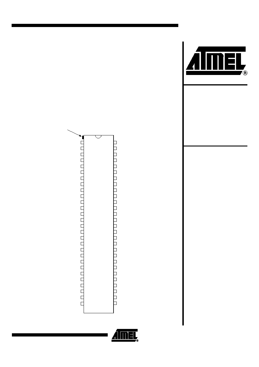
56 lead 0.6" DIL Package
Description
Atmel's TH7834C is a linear sensor based on charge-coupled device (CCD) technol-
ogy. It can be used in a wide range of applications thanks to operating mode flexibility,
very high definition and high dynamic range (document scanning, digital photography,
Art, Industrial and Scientific Applications).
1
2
3
4
5
6
7
8
9
10
11
12
13
14
15
16
17
18
19
20
21
22
23
24
25
26
27
28
56
55
54
53
52
51
50
49
48
47
46
45
44
43
42
41
40
39
38
37
36
35
34
33
32
31
30
29
VOS2
VDR2
VS2
VDD1-2
VSS
LS1-2
VA1-2
P1-2
VSS
3D
1D
4D
2D
VSS
VSS
2B
4B
1B
3B
VSS
VGS3-4
A3-4
VST
VSS
R3-4
VS4
VDR4
VOS4
VOS1
VDR1
VS1
R1-2
VSS
VST
A1-2
VGS1-2
VS
3A
1A
4A
2A
VSS
VSS
2C
4C
1C
3C
VSS
P3-4
VA3-4
LS3-4
VSS
VDD3-4
VS3
VDR3
VOS3
TOP VIEW
Pixel 1
mark
Very High-
resolution
Linear CCD
Image Sensor
(12000 Pixels)
TH7834C
Rev. 1997A¡IMAGE¡05/02
2
TH7834C
1997A¡IMAGE¡05/02
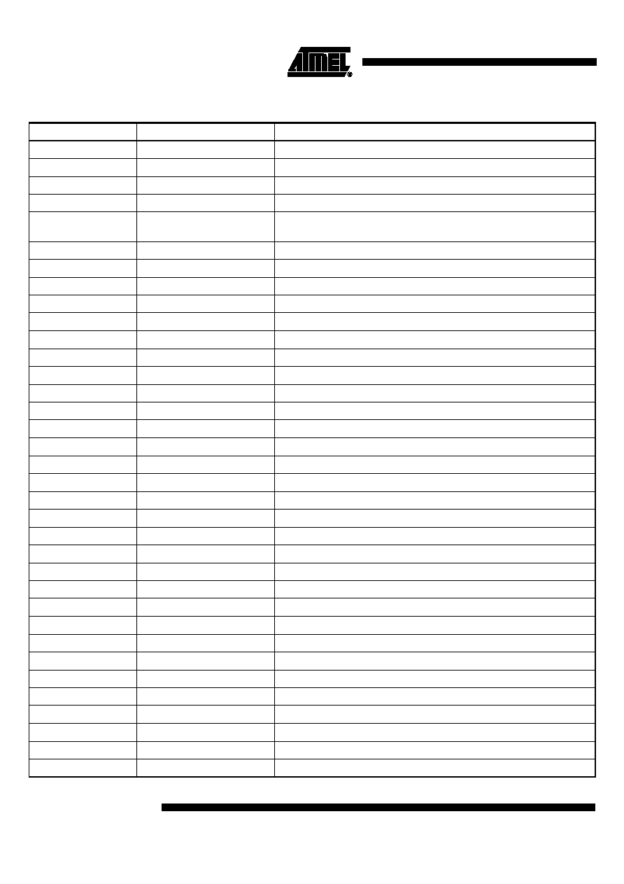
Pin Description
Pin Number
Symbol
Designation
1
V
OS1
Output 1 (Odd Pixels)
2
V
DR1
Reset DC Bias (Output 1)
3
V
S1
Amplifier Source Bias (Output 1)
4
R1-2
Reset Clock (Outputs 1 and 2)
5, 9, 14, 15, 20, 24, 33,
37, 42, 43, 48, 52
V
SS
Substrate Bias (Ground)
6, 34
VST
Pixel Storage Gate DC Bias
7
A1-2
Antiblooming and/or Exposure Time Control
8
V
GS1-2
Output Gate DC Bias
10
3A
Register Main Transport Clock
11
1A
Register Main Transport Clock
12
4A
Register Main Transport Clock
13
2A
Register Main Transport Clock
16
2C
Register Main Transport Clock
17
4C
Register Main Transport Clock
18
1C
Register Main Transport Clock
19
3C
Register Main Transport Clock
21
P3-4
Transfer Clock
22
VA
3-4
Antiblooming Diode Bias
23
LS3-4
Register End Transport Clock
25
V
DD3-4
Amplifier Drain Supplies (Outputs 3, 4)
26
V
S3
Amplifier Source Bias (Output 3)
27
V
DR3
Reset DC Bias (Output 3)
28
V
OS3
Output 3 (Odd Pixels)
29
V
OS4
Output 4 (Even Pixels)
30
V
DR4
Reset DC Bias (Output 4)
31
V
S4
Amplifier Source Bias (Output 4)
32
R3-4
Reset Clock (Outputs 3 and 4)
35
A3-4
Antiblooming and/or Exposure Time Control
36
V
GS3-4
Output Gate DC Bias
38
3D
Register Main Transport Clock
39
1D
Register Main Transport Clock
40
4D
Register Main Transport Clock
41
2D
Register Main Transport Clock
44
2B
Register Main Transport Clock
45
4B
Register Main Transport Clock

3
TH7834C
1997A¡IMAGE¡05/02
Notes:
1. Pins
A1-2
, V
GS1-2
,
P1-2
, VA
1-2
,
LS1-2
, V
DD1-2
,
R1-2
and respectively,
A3-4
, V
GS3-4
,
P3-4
, VA
3-4,
LS3-4
, V
DD3-4
,
R3-4
are not
connected together inside the package.
2. Two Pins V
ST
connected together inside the package.
Figure 1. TH7834 Block Diagram
Description
TH7834C high resolution linear array consists of 12000 useful pixel photosensitive line,
associated with four CCD shift registers and four output amplifiers. Transfer gates on
both sides of the photosensitive line enable delivery of charges, respectively:
À
on one side, charge accumulated by odd pixels (1, 3, 5... 11999), to CCD shift
registers A and C,
À
on the other side, charge accumulated by even pixels (2, 4, 6... 12000), to CCD
shift registers B and D.
Shift registers 1 and 2 collect charges generated by one half of the photosensitive line
(pixel 1 to 6000), whereas shift registers 3 and 4 collect charges generated by the sec-
ond half of the photosensitive line (pixels 12000 to 6001).
46
1B
Register Main Transport Clock
47
3B
Register Main Transport Clock
49
P1-2
Transfer Clock
50
VA
1-2
Antiblooming Diode Bias
51
LS1-2
Register End Transport Clock
53
V
DD1-2
Amplifier Drain Supplies (Outputs 1, 2)
54
V
S2
Amplifier Source Bias (Output 2)
55
V
DR2
Reset DC Bias (Output 2)
56
V
OS2
Output 2 (Even Pixels)
Pin Description (Continued)
Pin Number
Symbol
Designation
2B
2A
LS1-2
VDR2
VDR4
VS2
VS4
P1-2
VDD1-2
R1-2
P3-4
VDD3-4
R3-4
VST
VST
VGS1-2
VDR1
VDR3
VS1
VS3
VOS1
VOS3
CCD A
CCD C
VOS2
VOS4
CCD B
1
CCD D
12000
3D
3C
VGS3-4
LS3-4
4B
4A
1D
1C
1B
1A
4D
4C
3B
3A
2D
2C
4
TH7834C
1997A¡IMAGE¡05/02
The four CCD shift registers have separated clocks. The output signal can be, then,
delivered simultaneously or sequentially on the four outputs.
The four CCD shift registers are designed with 4 separated gates. According to the gate
connection, the signal can be read through 2 or 4 output amplifiers.
According to gate connection, 2 or 4 output operating mode can be chosen. In the 4 out-
put operating mode, signals associated to the end pixels of the array (either pixels
number 1, 2 or pixels number 11999, 12000) are delivered first in time and signals corre-
sponding to the center of the line (pixels number 5999, 6000 and 6001, 6002) are
delivered last in time. Thus, external circuitry and processing are needed to combine the
four video outputs and to restore the normal order of the pixels in accordance with their
spatial distribution on the photosensitive line.
Terminal stages for every CCD shift register have separate clock control inputs in order
to speed up the final charge to voltage conversion and reduce the video output settling
time.
Antiblooming and exposure time control functions are provided.
Symmetrical TH7834 package PIN OUT allow to inverted pin 1 and 56 positions without
damage.
To obtain optimal operating mode, separated driving circuits are recommended for each
readout shift register (at least
LS and
R).
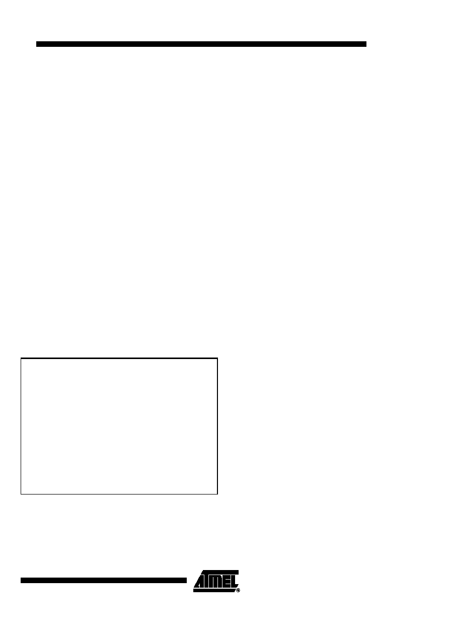
Figure 2. Driving Schematic
VOS1
VOS3
CCD A
CCD C
VOS2
VOS4
CCD B
2
6000
5999
6002
6001
11999
12000
1
Photosensitive line
CCD D
PHI3C
Pins
(1,2,3,4)B
Pins
(1,2,3,4)A
F
Pins
(1,2,3,4)D
Pins
(1,2,3,4)C
F
L1
L1
L1
L1
Logical signal :
Logical signal :
Logical signal :
Logical signal :
L2
L2
L2
L2
5
TH7834C
1997A¡IMAGE¡05/02
Readout Shift Register
Clocking
All gates of the 4 CCD shift registers are separated, enabling two or four output readout
modes.
To select 2 or 4 outputs operating mode, register main transport gates must be con-
nected as described here after:
À
4 outputs mode:
V
OS1
:
L1
=
2A
+
3A
;
L2
=
1A
+
4A
V
OS2
:
L1
=
2B
+
3B
;
L2
=
1B
+
4B
V
OS3
:
L1
=
2C
+
3C
;
L2
=
1C
+
4C
V
OS4
:
L1
=
2D
+
3D
;
L2
=
1D
+
4D
À
2 output mode: V
OS
1 and V
OS2
:
V
OS1
:
L1
=
2A
+
3A
+
1C
+
2C
L2
=
1A
+
4A
+
3C
+
4C
V
OS2
:
L1
=
2B
+
3B
+
1D
+
2D
L2
=
1B
+
4B
+
3D
+
4D
À
2 output mode: V
OS3
and V
OS4
:
V
OS3
:
L1
=
1A
+
2A
+
2C
+
3C
L2
=
3A
+
4A
+
1C
+
4C
V
OS4
:
L1
=
1B
+
2B
+
2D
+
3D
L2
=
3B
+
4B +
1D
+
4D
Note:
In 2 output mode, the unused outputs can be connected as following:
À
LS
=
R
= V
GS
= 0V
À 10V < V
DR
< 15V
À V
DD
= 15V
À V
S
not connected in order to cancel unused output amplifiers power consumption.
Operating Range
Operating range defines the temperature limits between which the functionality is guar-
anteed: 0░C to 70░C.
Absolute Maximum Ratings*
Storage Temperature ................................... -55░C to + 150░C
*NOTICE:
Stresses above those listed under absolute max-
imum ratings may cause permanent device fail-
ure. Functionality at or above these limits is not
implied. Exposure to absolute maximum ratings
for extended periods may affect reliability.
Operating Temperature .................................
0░C to + 70░C
Thermal Cycling.........................................................15░C/mm
Maximum Voltage:
À Pins: 4, 6, 7, 8, 10, 11, 12, 13, 16, 17, 18,
19, 21, 23, 32, 34, 35, 36, 38, 39, 40, 41, 44,
45, 46, 47, 49, 51...............................................-0.3V to + 15V
À Pins: 2, 3, 22, 25, 26, 27, 30,
31, 50, 53, 54, 55............................................-0.3V to + 15.5V
À Pins: 5, 9, 14, 15, 20, 24, 33, 37, 42, 43, 48, 52 .. Ground 0V