Rev. B - 30-Mar-01
1
Preliminary
T89C51RB2/RC2
8-bit Microcontroller with 16 Kbytes/ 32 Kbytes FLASH
1. Description
T89C51RB2/RC2 is a high performance FLASH version
of the 80C51 8-bit microcontrollers. It contains a 16K
or 32Kbytes Flash memory block for program and data.
The 16 Kbytes or 32 Kbytes FLASH memory can be
programmed either in parallel mode or in serial mode
with the ISP capability or with software. The
programming voltage is internally generated from the
standard V
CC
pin.
The T89C51RB2/RC2 retains all features of the 80C52
with 256 bytes of internal RAM, a 7-source 4-level
interrupt controller and three timer/counters.
In addition, the T89C51RB2/RC2 has a Programmable
Counter Array, an XRAM of 1024 byte, a Hardware
Watchdog Timer, a Keyboard Interface, a SPI Interface,
a more versatile serial channel that facilitates
multiprocessor communication (EUART) and a speed
improvement mechanism (X2 mode).
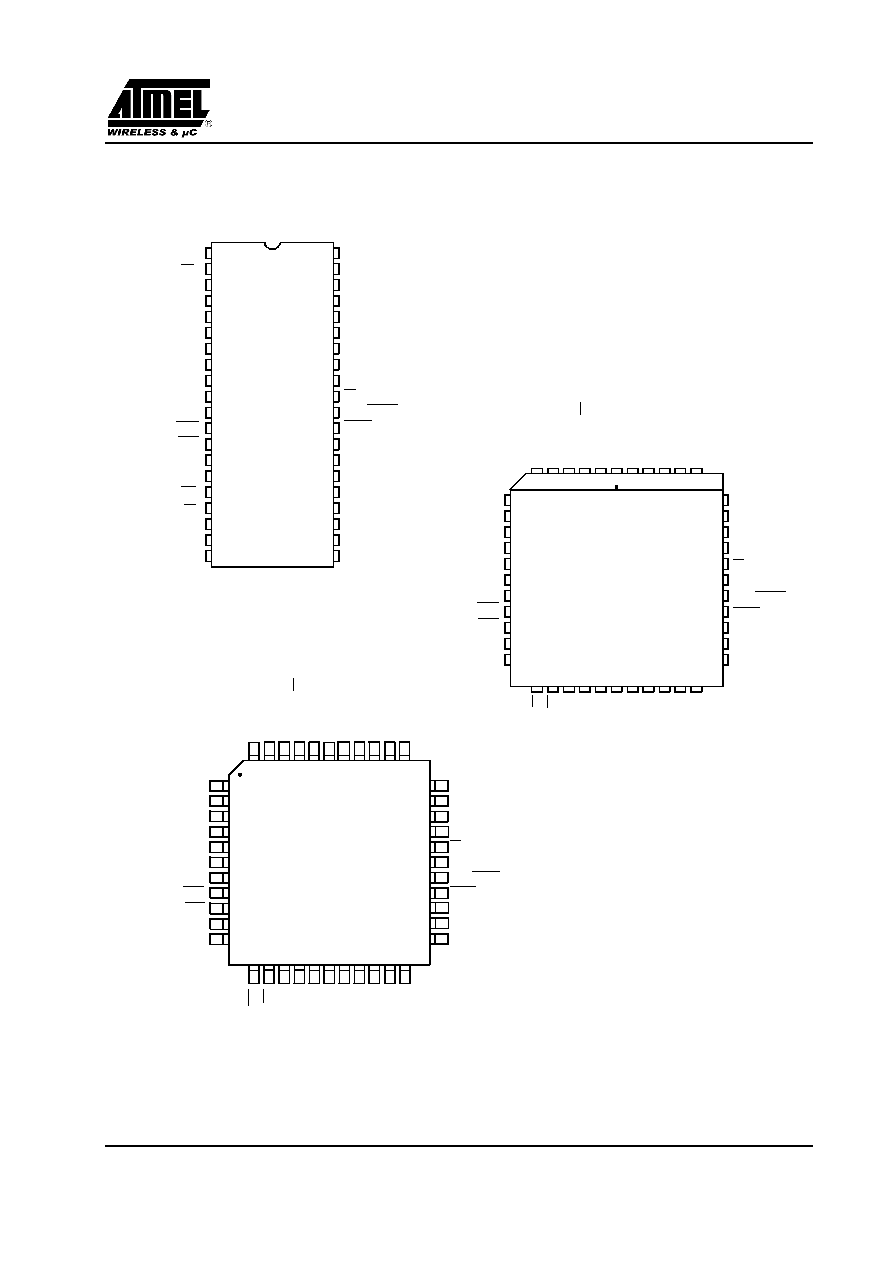
Pinout is the standard 40/44 pins of the C52.
The fully static design of the T89C51RB2/RC2 allows
to reduce system power consumption by bringing the
clock frequency down to any value, even DC, without
loss of data.
The T89C51RB2/RC2 has 2 software-selectable modes
of reduced activity and 8 bit clock prescaler for further
reduction in power consumption. In the Idle mode the
CPU is frozen while the peripherals and the interrupt
system are still operating. In the power-down mode the
RAM is saved and all other functions are inoperative.
The added features of the T89C51RB2/RC2 make it more
powerful for applications that need pulse width
modulation, high speed I/O and counting capabilities
such as alarms, motor control, corded phones, smart card
readers.
2. Features
�
80C52 Compatible
� 8051 pin and instruction compatible
� Four 8-bit I/O ports
� Three 16-bit timer/counters
� 256 bytes scratch pad RAM
� 10 Interrupt sources with 4 priority levels
� Dual Data Pointer
�
Variable length MOVX for slow RAM/peripherals
�
ISP (In System Programming) using standard V
CC
power supply.
�
Boot ROM contains low level FLASH programming
routines and a default serial loader
�
High-Speed Architecture
� 40 MHz in standard mode
� 20 MHz in X2 mode (6 clocks/machine cycle)
�
16K/32K bytes on-chip FLASH program / data
Memory
� Byte and page (128 bytes) erase and write
� 100k write cycles
�
On-chip 1024 bytes expanded RAM (XRAM)
� Software selectable size (0, 256, 512, 768, 1024
bytes)
� 256 bytes selected at reset for TS87C51RB2/RC2
compatibility
�
Keyboard interrupt interface on port P1
�
SPI Interface (Master / Slave Mode)
�
8-bit clock prescaler
�
Improved X2 mode with independant selection for
CPU and each peripheral
�
Programmable Counter Array 5 Channels with:
� High Speed Output,
� Compare / Capture,
� Pulse Width Modulator,
� Watchdog Timer Capabilities
�
Asynchronous port reset
�
Full duplex Enhanced UART
�
Dedicated Baud Rate Generator for UART
�
Low EMI (inhibit ALE)
2
Rev. B - 30-Mar-01
Preliminary
T89C51RB2/RC2
�
Hardware Watchdog Timer (One-time enabled with Reset-Out)
�
Power control modes:
� Idle Mode.
� Power-down mode.
- 50
�A at 3V
- 100
�A Commercial at 5V
- 150
�A Industrial at 5V
� Power-Off Flag.
�
Power supply: 4.5 to 5.5V or 2.7 to 3.6V
�
Temperature ranges: Commercial (0 to +70
�C) and industrial (-40�C to +85�C).
�
Packages: PDIL40, PLCC44, VQFP44
Table 1. Memory Size
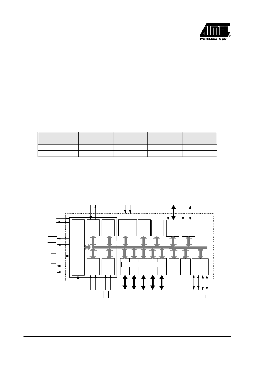
3. Block Diagram
Flash (bytes)
XRAM (bytes)
TOTAL RAM
(bytes)
I/O
T89C51RB2
16k
1024
1280
32
T89C51RC2 32k
1024
1280
32
Timer 0
INT
RAM
256x8
T0
T1
Rx
D
Tx
D
WR
RD
EA
PSEN
ALE/
XTAL2
XTAL1
EUART
CPU
Timer 1
IN
T
1
Ctrl
IN
T
0
(2)
(2)
C51
CORE
(2) (2)
(2) (2)
Port 0
P0
Port 1 Port 2 Port 3
Parallel I/O Ports & Ext. Bus
P1
P2
P3
XRAM
1Kx8
IB-bus
PCA
RE
S
E
T
PROG
Watch
Dog
PC
A
EC
I
Vs
s
V
CC
(2)
(2)
(1)
(1): Alternate function of Port 1
(2): Alternate function of Port 3
(1)
Timer2
T2
EX
T2
(1)
(1)
Port I2
PI
2
Flash
32Kx8 or
16Kx8
Key
Board
ROM
2Kx8
Boot
+
BRG
SPI
MIS
O
MO
S
I
SC
K
(1) (1) (1)
SS
(1)
Rev. B - 30-Mar-01
3
Preliminary
T89C51RB2/RC2
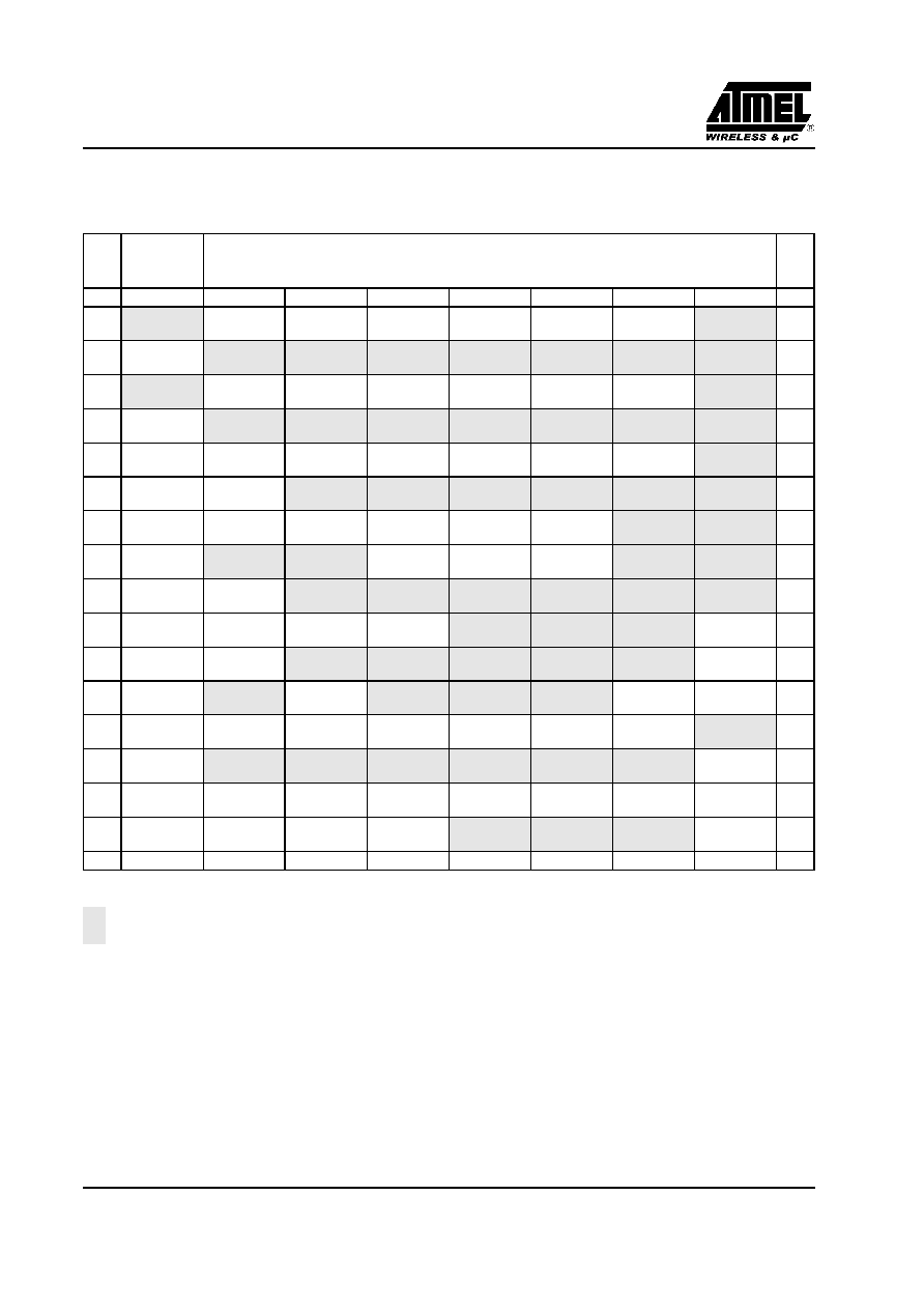
4. SFR Mapping
The Special Function Registers (SFRs) of the T89C51RB2/RC2 fall into the following categories:
� C51 core registers: ACC, B, DPH, DPL, PSW, SP
� I/O port registers: P0, P1, P2, P3
� Timer registers: T2CON, T2MOD, TCON, TH0, TH1, TH2, TMOD, TL0, TL1, TL2, RCAP2L, RCAP2H
� Serial I/O port registers: SADDR, SADEN, SBUF, SCON
� PCA ( Programmable Counter Array ) registers : CCON , CCAPMx , CL , CH , CCAPxH , CCAPxL (x : 0 to 4)
� Power and clock control registers: PCON
� Hardware Watchdog Timer registers : WDTRST, WDTPRG
� Interrupt system registers: IE0, IPL0, IPH0 , IE1 , IPL1 , IPH1
� Keyboard Interface registers : KBE , KBF , KBLS
� SPI registers : SPCON , SPSTR , SPDAT
� BRG ( Baud Rate Generator ) registers : BRL , BDRCON
� Flash register : FCON
� Clock Prescaler register : CKRL
� Others: AUXR, AUXR1 , CKCON0 , CKCON1