Rev. 4563C¡ISM¡01/04
Features
À
Single 3-V Supply Voltage
À
High-power-added Efficient Power Amplifier (P
out
Typically 28 dBm)
À
Ramp-controlled Output Power
À
Low-noise Preamplifier (NF Typically 2.1 dB)
À
Biasing for External PIN Diode T/R Switch
À
Current-saving Standby Mode
À
Few External Components
À
Package: QFN20
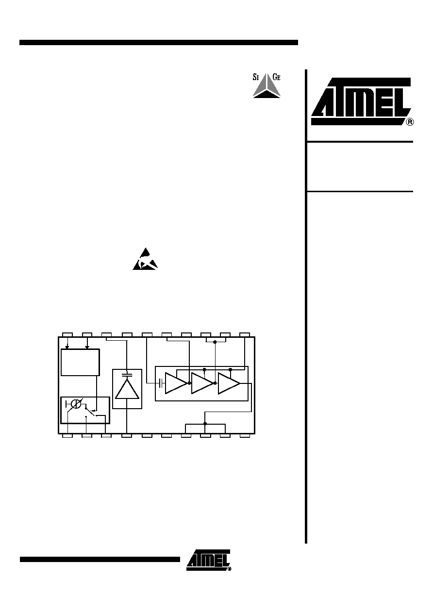
Description
The T7026 is a monolithic SiGe transmit/receive front-end IC with power amplifier,
low-noise amplifier and T/R switch driver. It is especially designed for operation in
TDMA systems like DECT, IEEE 802.11 FHSS WLAN, home RF and ISM proprietary
radios. Due to the ramp-control feature and a very low quiescent current, an external
switch transistor for V
S
is not required.
Electrostatic sensitive device.
Observe precautions for handling.
Figure 1. Block Diagram
G
N
D
V
2
_
P
A
V
1
_
P
A
V
S
_
L
N
A
V
3
_
P
A
_
O
U
T
L
N
A
_
I
N
P
A
_
I
N
V
2
_
P
A
G
N
D
R
A
M
P
G
N
D
P
U
TX/RX
standby
control
LNA
PA
R
X
_
O
N
L
N
A
_
O
U
T
G
N
D
R
_
S
W
I
T
C
H
S
W
I
T
C
H
_
O
U
T
_
R
X
SiGe FE
TX
V
3
_
P
A
_
O
U
T
V
3
_
P
A
_
O
U
T
T7026
S
W
I
T
C
H
_
O
U
T
_
T
X
ISM 2.4 GHz
Front End IC
T7026
2
T7026
4563C¡ISM¡01/04
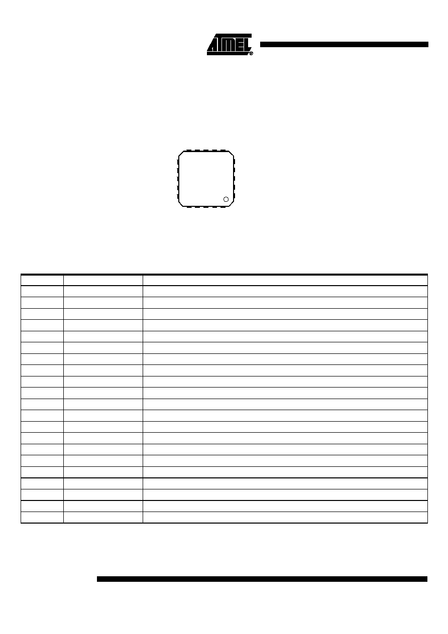
Pin Configuration
Figure 2. Pinning QFN20
1
2
3
4
5
15
14
13
12
11
10
6
7
8
9
16
20
19
18
17
RX_ON
R_SWITCH
SWITCH_OUT_RX
SWITCH_OUT_TX
GND_LNA1
V
3
_
P
A
_
O
U
T
V
3
_
P
A
_
O
U
T
V
3
_
P
A
_
O
U
T
G
N
D
_
L
N
A
2
L
N
A
_
I
N
V2_PA
V2_PA
GND
V1_PA
NC
R
A
M
P
P
A
_
I
N
V
S
_
L
N
A
L
N
A
_
O
U
T
P
U
T7026
Pin Description
Pin
Symbol
Function
1
RX_ON
RX active high
2
R_SWITCH
Resistor to GND sets the PIN diode current
3
SWITCH_OUT_RX
Switched current output for PIN diode (active in RX mode)
4
SWITCH_OUT_TX
Switched current output for PIN diode (active in TX mode)
5
GND_LNA1
Ground
6
LNA_IN
Low-noise amplifier input
7
GND_LNA2
Ground
8
V3_PA_OUT
Inductor to power supply and matching network for power amplifier output
9
V3_PA_OUT
Inductor to power supply and matching network for power amplifier output
10
V3_PA_OUT
Inductor to power supply and matching network for power amplifier output
11
V2_PA
Inductor to power supply for power amplifier
12
V2_PA
Inductor to power supply for power amplifier
13
GND
Ground
14
V1_PA
Supply voltage for power amplifier
15
NC
Not connected
16
RAMP
Power ramping control input
17
PA_IN
Power amplifier input
18
VS_LNA
Supply voltage input for low-noise amplifier
19
LNA_OUT
Low-noise amplifier output
20
PU
Power-up active high
Slug
GND
Ground

3
T7026
4563C¡ISM¡01/04
Absolute Maximum Ratings
Stresses beyond those listed under "Absolute Maximum Ratings" may cause permanent damage to the device. This is a stress rating
only and functional operation of the device at these or any other conditions beyond those indicated in the operational sections of this
specification is not implied. Exposure to absolute maximum rating conditions for extended periods may affect device reliability.
All voltages are referred to ground (pins GND and slug)
Parameters
Symbol
Value
Unit
Supply voltage
Pins VS_LNA, V1_PA, V2_PA and
V3_PA_OUT, no RF
V
S
5
V
Junction temperature
T
j
150
░C
Storage temperature
T
stg
-40 to +125
░C
RF input power LNA
P
inLNA
-5 dBm
dBm
RF input power PA
P
inPA
10 dBm
dBm
Thermal Resistance
Parameters
Symbol
Value
Unit
Junction ambient QFN20, slug soldered on
PCB
R
thJA
27
K/W
Operating Range
All voltages are referred to ground (pins GND and slug). Power supply points are VS_LNA, V1_PA, V2_PA, V3_PA_OUT. The following
table represents the sum of all supply currents depending on the TX/RX mode.
Parameters
Symbol
Min.
Typ.
Max.
Unit
Supply voltage
Pins V1_PA, V2_PA and V3_PA_OUT
V
S
2.7
3.6
4.6
V
Supply voltage Pin VS_LNA
V
S
2.7
3.0
5.5
V
Supply current
TX
RX
I
S
I
S
470
8
mA
mA
Standby current PU = 0
I
S
10
ÁA
Ambient temperature
T
amb
-25
+25
+70
░C
4
T7026
4563C¡ISM¡01/04
Electrical Characteristics
Test conditions (unless otherwise specified): V
S
= 3.6 V, T
amb
= 25░C
Parameters
Test Conditions
Symbol
Min.
Typ.
Max.
Unit
Power Amplifier
(1)
Supply voltage
Pins V1_PA, V2_PA and
V3_PA_OUT
V
S
2.7
3.6
4.6
V
Supply current
TX
I
S_TX
470
mA
RX (PA off), V
RAMP
ú
0.1 V
I
S_RX
10
ÁA
Standby current
Standby for V
RAMP
ú
0.1 V
I
S_standby
10
ÁA
Frequency range
TX
f
2.4
2.5
GHz
Gain-control range
TX
D
Gp
60
42
dB
Power gain maximum
TX
Pin PA_IN to V3_PA_OUT
Gp
28
34
33
dB
Power gain minimum
Gp
-40
-17
dB
Ramping voltage maximum
TX, power gain (max), pin RAMP
V
RAMP max
1.6
1.65
1.7
V
Ramping voltage minimum
TX, power gain (min), pin RAMP
V
RAMP min
1
V
Ramping current maximum
TX, V
RAMP
= 1.75 V, pin RAMP
I
RAMP max
0.1
mA
Power-added efficiency
TX
PAE
33
37
%
Saturated output power
TX, input power = 0 dBm referred to
pins V3_PA_OUT
P
sat
27
28
29
dBm
Input matching
(2)
TX pin PA_IN
Load
VSWR
< 1.5:1
Output matching
(2)
TX pins V3_PA_OUT
Load
VSWR
< 1.5:1
Harmonics at P 1dBCP
TX pins V3_PA_OUT
2 fo
-30
dBc
Harmonics at P 1dBCP
TX pins V3_PA_OUT
3 fo
-30
dBc
T/R-switch Driver (Current Programming by External Resistor from R_SWITCH to GND)
Switch-out current output
Standby, pin SWITCH_OUT
I
S_O_standby
1
ÁA
RX
I
S_O_RX
1
ÁA
TX at 100
W
I
S_O_100
1.7
mA
TX at 1.2 k
W
I
S_O_1k2
7
mA
TX at 33 k
W
I
S_O_33k
17
mA
TX at R switch open
I
S_O_R
19
mA
I_Switch_Out_RX maximum
7
mA
Low-noise Amplifier
(3)
Supply voltage
All, pin VS_LNA
V
S
2.7
3.0
5
V
Supply current
RX
I
S
8
10
mA
Supply current
(LNA and control logic)
TX (control logic active)
pin VS_LNA
I
S
0.5
mA
Standby current
Standby, pin VS_LNA
I
S_standby
1
10
ÁA
Frequency range
RX
f
2.4
2.5
GHz
Notes:
1. Power amplifier shall be unconditionally stable, maximum duty cycle 100%, true cw operation, maximum load mismatch
and duration: VSWR = 8:1 (all phases) 10 s, ZG = 50
W
, V
S
= 3.6 V.
2. With external matching network, load impedance 50
W
.
3. Low-noise amplifier shall be unconditionally stable.
4. With external matching components.
5
T7026
4563C¡ISM¡01/04
Power gain
RX, pin LNA_IN to LNA_OUT
Gp
15
16
19
dB
Noise figure
RX
NF
2.1
2.3
dB
Gain compression
RX, referred to pin LNA_OUT
O1dB
-9
-7
-6
dBm
Third-order input interception point
RX
IIP3
-16
-14
-13
dBm
Input matching
(4)
RX, pin LNA_IN
VSWRin
< 2:1
Output matching
(4)
RX, pin LNA_OUT
VSWRout
< 2:1
Logic Input Levels (RX_ON, PU)
High input level
= `1', pins RX_ON and PU
V
iH
2.4
V
S, LNA
V
Low input level
= `0'
V
iL
0
0.5
V
High input current
= `1', V
iH
= 2.4 V
I
iH
40
60
ÁA
Low input current
= `0'
I
iL
0.2
ÁA
Electrical Characteristics (Continued)
Test conditions (unless otherwise specified): V
S
= 3.6 V, T
amb
= 25░C
Parameters
Test Conditions
Symbol
Min.
Typ.
Max.
Unit
Notes:
1. Power amplifier shall be unconditionally stable, maximum duty cycle 100%, true cw operation, maximum load mismatch
and duration: VSWR = 8:1 (all phases) 10 s, ZG = 50
W
, V
S
= 3.6 V.
2. With external matching network, load impedance 50
W
.
3. Low-noise amplifier shall be unconditionally stable.
4. With external matching components.
Control Logic for LNA and T/R-switch Driver
Operation Mode
PU
RX_ON
Standby
0
0
TX
1
0
RX
1
1