
1
Features
À
High-density, High-performance, Electrically-erasable Complex Programmable
Logic Device
¡ 32 Macrocells
¡ 5 Product Terms per Macrocell, Expandable up to 40 per Macrocell
¡ 44 Pins
¡ 7.5 ns Maximum Pin-to-pin Delay
¡ Registered Operation up to 125 MHz
¡ Enhanced Routing Resources
À
In-System Programmability (ISP) via JTAG
À
Flexible Logic Macrocell
¡ D/T Latch Configurable Flip-flops
¡ Global and Individual Register Control Signals
¡ Global and Individual Output Enable
¡ Programmable Output Slew Rate
¡ Programmable Output Open Collector Option
¡ Maximum Logic Utilization by Burying a Register with a COM Output
À
Advanced Power Management Features
À
Automatic 10 ÁA Standby for "L" Version
À
Pin-controlled 1 mA Standby Mode
À
Programmable Pin-keeper Inputs and I/Os
À
Reduced-power Feature per Macrocell
À
Available in Commercial and Industrial Temperature Ranges
À
Available in 44-lead PLCC and TQFP
À
Advanced EEPROM Technology
¡ 100% Tested
¡ Completely Reprogrammable
¡ 10,000 Program/Erase Cycles
¡ 20-year Data Retention
¡ 2000V ESD Protection
¡ 200 mA Latch-up Immunity
À
JTAG Boundary-scan Testing to IEEE Std. 1149.1-1990 and 1149.1a-1993 Supported
À
PCI-compliant
À
Security Fuse Feature
Enhanced Features
À
Improved Connectivity (Additional Feedback Routing, Alternate Input Routing)
À
Output Enable Product Terms
À
D Latch Mode
À
Combinatorial Output with Registered Feedback within Any Macrocell
À
Three Global Clock Pins
À
ITD (Input Transition Detection) Circuits on Global Clocks, Inputs and I/O
("L" versions)
À
Fast Registered Input from Product Term
À
Programmable "Pin-keeper" Option
À
V
CC
Power-up Reset Option
À
Pull-up Option on JTAG Pins TMS and TDI
À
Advanced Power Management Features
¡ Input Transition Detection
¡ Power-down ("L" versions)
¡ Individual Macrocell Power Option
¡ Disable ITD on Global Clocks, Inputs and I/O
High-
performance
EEPROM CPLD
ATF1502AS
ATF1502ASL
Rev. 0995J¡PLD¡09/02
2
ATF1502AS(L)
0995J¡PLD¡09/02
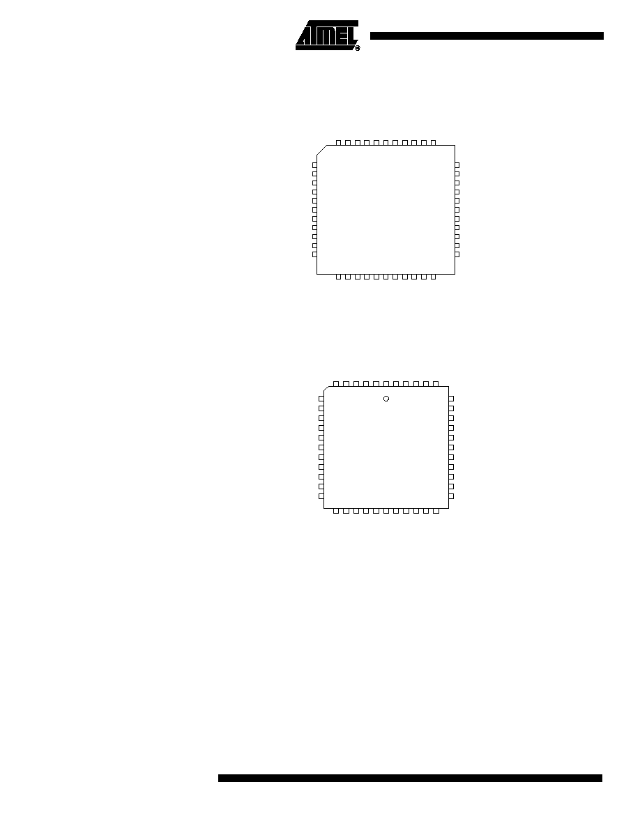
44-lead TQFP
Top View
44-lead PLCC
Top View
Description
The ATF1502AS is a high-performance, high-density complex programmable logic device
(CPLD) that utilizes Atmel's proven electrically-erasable technology. With 32 logic macrocells
and up to 36 inputs, it easily integrates logic from several TTL, SSI, MSI, LSI and classic
PLDs. The ATF1502AS's enhanced routing switch matrices increase usable gate count and
the odds of successful pin-locked design modifications.
The ATF1502AS has up to 32 bi-directional I/O pins and four dedicated input pins, depending
on the type of device package selected. Each dedicated pin can also serve as a global control
signal, register clock, register reset or output enable. Each of these control signals can be
selected for use individually within each macrocell.
1
2
3
4
5
6
7
8
9
10
11
33
32
31
30
29
28
27
26
25
24
23
I/O/TDI
I/O
I/O
GND
PD1/I/O
I/O
TMS/I/O
I/O
VCC
I/O
I/O
I/O
I/O/TDO
I/O
I/O
VCC
I/O
I/O
I/O/TCK
I/O
GND
I/O
44
43
42
41
40
39
38
37
36
35
34
12
13
14
15
16
17
18
19
20
21
22
I/O
I/O
I/O
I/O
GND
VCC
I/O
PD2/I/O
I/O
I/O
I/O
I/O
I/O
I/O
VCC
GCLK2/OE2/I
GCLR/I
I/OE1
GCLK1/I
GND
GCLK3/I/O
I/O
7
8
9
10
11
12
13
14
15
16
17
39
38
37
36
35
34
33
32
31
30
29
TDI/I/O
I/O
I/O
GND
PD1/I/O
I/O
I/O/TMS
I/O
VCC
I/O
I/O
I/O
I/O/TDO
I/O
I/O
VCC
I/O
I/O
I/O/TCK
I/O
GND
I/O
6
5
4
3
2
1
44
43
42
41
40
18
19
20
21
22
23
24
25
26
27
28
I/O
I/O
I/O
I/O
GND
VCC
I/O
PD2/I/O
I/O
I/O
I/O
I/O
I/O
I/O
VCC
GCLK2/OE2/I
GCLR/I
OE1/I
GCLK1/I
GND
GCLK3/I/O
I/O
3
ATF1502AS(L)
0995J¡PLD¡09/02
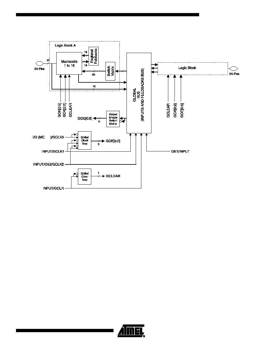
Block Diagram
Each of the 32 macrocells generates a buried feedback that goes to the global bus. Each input
and I/O pin also feeds into the global bus. The switch matrix in each logic block then selects 40
individual signals from the global bus. Each macrocell also generates a foldback logic term
that goes to a regional bus. Cascade logic between macrocells in the ATF1502AS allows fast,
efficient generation of complex logic functions. The ATF1502AS contains four such logic
chains, each capable of creating sum term logic with a fan-in of up to 40 product terms.
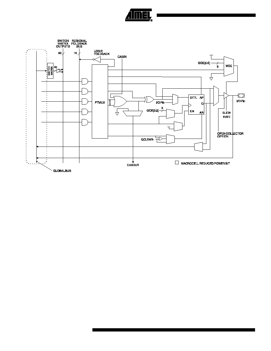
The ATF1502AS macrocell, shown in Figure 1, is flexible enough to support highly complex
logic functions operating at high speed. The macrocell consists of five sections: product terms
and product term select multiplexer, OR/XOR/CASCADE logic, a flip-flop, output select and
enable, and logic array inputs.
Unused product terms are automatically disabled by the compiler to decrease power con-
sumption. A security fuse, when programmed, protects the contents of the ATF1502AS. Two
bytes (16 bits) of User Signature are accessible to the user for purposes such as storing
project name, part number, revision or date. The User Signature is accessible regardless of
the state of the security fuse.
The ATF1502AS device is an in-system programmable (ISP) device. It uses the industry stan-
dard 4-pin JTAG interface (IEEE Std. 1149.1), and is fully compliant with JTAG's Boundary-
scan Description Language (BSDL). ISP allows the device to be programmed without remov-
ing it from the printed circuit board. In addition to simplifying the manufacturing flow, ISP also
allows design modifications to be made in the field via software.
B
32
4
ATF1502AS(L)
0995J¡PLD¡09/02
Figure 1. ATF1502AS Macrocell
Product Terms and
Select Mux
Each ATF1502AS macrocell has five product terms. Each product term receives as its inputs
all signals from both the global bus and regional bus.
The product term select multiplexer (PTMUX) allocates the five product terms as needed to
the macrocell logic gates and control signals. The PTMUX programming is determined by the
design compiler, which selects the optimum macrocell configuration.
OR/XOR/
CASCADE Logic
The ATF1502AS's logic structure is designed to efficiently support all types of logic. Within a
single macrocell, all the product terms can be routed to the OR gate, creating a 5-input
AND/OR sum term. With the addition of the CASIN from neighboring macrocells, this can be
expanded to as many as 40 product terms with little additional delay.
The macrocell's XOR gate allows efficient implementation of compare and arithmetic func-
tions. One input to the XOR comes from the OR sum term. The other XOR input can be a
product term or a fixed high or low level. For combinatorial outputs, the fixed level input allows
polarity selection. For registered functions, the fixed levels allow DeMorgan minimization of
product terms. The XOR gate is also used to emulate T- and JK-type flip-flops.
Flip-flop
The ATF1502AS's flip-flop has very flexible data and control functions. The data input can
come from either the XOR gate, from a separate product term or directly from the I/O pin.
Selecting the separate product term allows creation of a buried registered feedback within a
combinatorial output macrocell. (This feature is automatically implemented by the fitter soft-
ware). In addition to D, T, JK and SR operation, the flip-flop can also be configured as a flow-
through latch. In this mode, data passes through when the clock is high and is latched when
the clock is low.

5
ATF1502AS(L)
0995J¡PLD¡09/02
The clock itself can be either one of the Global CLK signals (GCK[0 : 2]) or an individual prod-
uct term. The flip-flop changes state on the clock's rising edge. When the GCK signal is used
as the clock, one of the macrocell product terms can be selected as a clock enable. When the
clock enable function is active and the enable signal (product term) is low, all clock edges are
ignored. The flip-flop's asynchronous reset signal (AR) can be either the Global Clear
(GCLEAR), a product term, or always off. AR can also be a logic OR of GCLEAR with a prod-
uct term. The asynchronous preset (AP) can be a product term or always off.
Extra Feedback
The ATF1502AS(L) macrocell output can be selected as registered or combinatorial. The
extra buried feedback signal can be either combinatorial or a registered signal regardless of
whether the output is combinatorial or registered. (This enhancement function is automatically
implemented by the fitter software.) Feedback of a buried combinatorial output allows the cre-
ation of a second latch within a macrocell.
I/O Control
The output enable multiplexer (MOE) controls the output enable signal. Each I/O can be indi-
vidually configured as an input, output or for bi-directional operation. The output enable for
each macrocell can be selected from the true or compliment of the two output enable pins, a
subset of the I/O pins, or a subset of the I/O macrocells. This selection is automatically done
by the fitter software when the I/O is configured as an input, all macrocell resources are still
available, including the buried feedback, expander and cascade logic.
Global Bus/Switch
Matrix
The global bus contains all input and I/O pin signals as well as the buried feedback signal from
all 32 macrocells. The switch matrix in each logic block receives as its inputs all signals from
the global bus. Under software control, up to 40 of these signals can be selected as inputs to
the logic block.
Foldback Bus
Each macrocell also generates a foldback product term. This signal goes to the regional bus
and is available to four macrocells. The foldback is an inverse polarity of one of the macrocell's
product terms. The four foldback terms in each region allow generation of high fan-in sum
terms (up to nine product terms) with little additional delay.
Programmable
Pin-keeper
Option for
Inputs and I/Os
The ATF1502AS offers the option of programming all input and I/O pins so that pin-keeper cir-
cuits can be utilized. When any pin is driven high or low and then subsequently left floating, it
will stay at that previous high or low level. This circuitry prevents unused input and I/O lines
from floating to intermediate voltage levels, which causes unnecessary power consumption
and system noise. The keeper circuits eliminate the need for external pull-up resistors and
eliminate their DC power consumption.