1
Features
·
Low-voltage and Standard-voltage Operation
2.7 (V
CC
= 2.7V to 5.5V)
1.8 (V
CC
= 1.8V to 5.5V)
·
User Selectable Internal Organization
16K: 2048 x 8 or 1024 x 16
·
3-wire Serial Interface
·
Sequential Read Operation
·
Schmitt Trigger, Filtered Inputs for Noise Suppression
·
2 MHz Clock Rate (5V) Compatibility
·
Self-timed Write Cycle (10 ms max)
·
High Reliability
Endurance: 1 Million Write Cycles
Data Retention: 100 Years
·
Automotive Grade, Extended Temperature and Lead-Free/Halogen-Free
Devices Available
·
8-lead PDIP, 8-lead JEDEC SOIC, 8-lead MAP and 8-lead TSSOP Packages
Description
The AT93C86A provides 16384 bits of serial electrically erasable programmable read
only memory (EEPROM) organized as 1024 words of 16 bits each when the ORG Pin
is connected to V
CC
and 2048 words of 8 bits each when it is tied to ground. The
device is optimized for use in many industrial and commercial applications where low
power and low voltage operations are essential. The AT93C86A is available in space
saving 8-lead PDIP, 8-lead JEDEC SOIC, 8-lead MAP and 8-lead TSSOP packages.
3-wire Serial
EEPROM
16K
(2048 x 8 or 1024 x 16)
AT93C86A
Preliminary
Rev. 3408CSEEPR1/04
Pin Configurations
Pin Name
Function
CS
Chip Select
SK
Serial Data Clock
DI
Serial Data Input
DO
Serial Data Output
GND
Ground
VCC
Power Supply
ORG
Internal Organization
DC
Don't Connect
8-lead PDIP
1
2
3
4
8
7
6
5
CS
SK
DI
DO
VCC
DC
ORG
GND
8-lead SOIC
1
2
3
4
8
7
6
5
CS
SK
DI
DO
VCC
DC
ORG
GND
8-lead TSSOP
1
2
3
4
8
7
6
5
CS
SK
DI
DO
VCC
DC
ORG
GND
8-lead MAP
Bottom View
1
2
3
4
8
7
6
5
VCC
DC
ORG
GND
CS
SK
DI
DO
2
AT93C86A [Preliminary]
3408CSEEPR1/04
The AT93C86A is enabled through the Chip Select pin (CS), and accessed via a 3-wire
serial interface consisting of Data Input (DI), Data Output (DO), and Shift Clock (SK).
Upon receiving a READ instruction at DI, the address is decoded and the data is
clocked out serially on the data output pin DO. The WRITE cycle is completely self-
timed and no separate ERASE cycle is required before WRITE. The WRITE cycle is
only enabled when the part is in the ERASE/WRITE ENABLE state. When CS is brought
"high" following the initiation of a WRITE cycle, the DO pin outputs the READY/BUSY
status of the part. The AT93C86A is available in a 2.7V to 5.5V version.
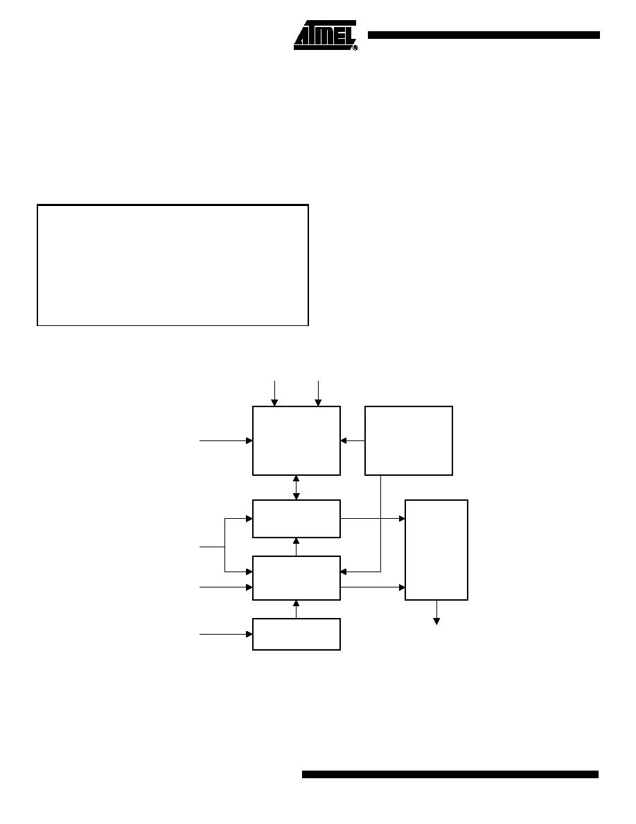
Block Diagram
Note:
1. When the ORG pin is connected to Vcc, the x 16 organization is selected. When it is connected to ground, the x 8 organiza-
tion is selected. If the ORG pin is left unconnected and the application does not load the input beyond the capability of the
internal 1 Meg ohm pullup, then the x 16 organization is selected. This feature is not available on the 1.8V devices.
Absolute Maximum Ratings*
Operating Temperature................................. -55
°
C to +125
°
C
*NOTICE:
Stresses beyond those listed under "Absolute
Maximum Ratings" may cause permanent dam-
age to the device. This is a stress rating only and
functional operation of the device at these or any
other conditions beyond those indicated in the
operational sections of this specification is not
implied. Exposure to absolute maximum rating
conditions for extended periods may affect
device reliability
Storage Temperature .................................... -65
°
C to +150
°
C
Voltage on any Pin
with Respect to Ground .....................................-1.0V to +7.0V
Maximum Operating Voltage .......................................... 6.25V
DC Output Current........................................................ 5.0 mA
ADDRESS
DECODER
OUTPUT
BUFFER
DO
ORG
DI
CS
SK
Vcc
GND
CLOCK
GENERATOR
MODE
DECODE
LOGIC
DATA
REGISTER
MEMORY ARRAY
2048 x 8
OR
1024 x 16
3
AT93C86A [Preliminary]
3408CSEEPR1/04
Note:
1. This parameter is characterized and is not 100% tested.
Note:
1. V
IL
min and V
IH
max are reference only and are not tested.
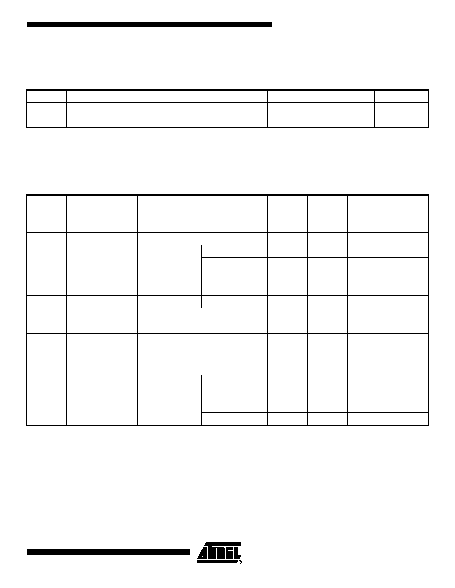
Pin Capacitance
(1)
Applicable over recommended operating range from T
A
= 25
°
C, f = 1.0 MHz, V
CC
= +5.0V (unless otherwise noted).
Symbol
Test Conditions
Max
Units
Conditions
C
OUT
Output Capacitance (DO)
5
pF
V
OUT
= 0V
C
IN
Input Capacitance (CS, SK, DI)
5
pF
V
IN
= 0V
DC Characteristics
Applicable over recommended operating range from: T
AI
= -40
°
C to +85
°
C, V
CC
= +1.8V to +5.5V,
T
AE
= -40
°
C to +125
°
C, V
CC
= +1.8V to +5.5V (unless otherwise noted).
Symbol
Parameter
Test Condition
Min
Typ
Max
Unit
V
CC1
Supply Voltage
1.8
5.5
V
V
CC2
Supply Voltage
2.7
5.5
V
V
CC3
Supply Voltage
4.5
5.5
V
I
CC
Supply Current
V
CC
= 5.0V
READ at 1.0 MHz
0.5
2.0
mA
WRITE at 1.0 MHz
0.5
2.0
mA
I
SB1
Standby Current
V
CC
= 1.8V
CS = 0V
0
0.1
µA
I
SB2
Standby Current
V
CC
= 2.7V
CS = 0V
6.0
10.0
µA
I
SB3
Standby Current
V
CC
= 5.0V
CS = 0V
17
30
µA
I
IL
Input Leakage
V
IN
= 0V to V
CC
0.1
3.0
µA
I
OL
Output Leakage
V
IN
= 0V to V
CC
0.1
3.0
µA
V
IL1
(1)
V
IH1
(1)
Input Low Voltage
Input High Voltage
2.7V
V
CC
5.5V
-0.6
2.0
0.8
V
CC
+ 1
V
V
IL2
(1)
V
IH2
(1)
Input Low Voltage
Input High Voltage
1.8V
V
CC
2.7V
-0.6
V
CC
x 0.7
V
CC
x 0.3
V
CC
+ 1
V
V
OL1
V
OH1
Output Low Voltage
Output High Voltage
2.7V
V
CC
5.5V
I
OL
= 2.1 mA
0.4
V
I
OH
= -0.4 mA
2.4
V
V
OL2
V
OH2
Output Low Voltage
Output High Voltage
1.8V
V
CC
2.7V
I
OL
= 0.15 mA
0.2
V
I
OH
= -100 µA
V
CC
- 0.2
V

4
AT93C86A [Preliminary]
3408CSEEPR1/04
Note:
1. This parameter is characterized and is not 100% tested.
AC Characteristics
Applicable over recommended operating range from T
AI
= -40°C to + 85°C, T
AE
= -40
°
C to +125
°
C, V
CC
= As Specified,
CL = 1 TTL Gate and 100 pF (unless otherwise noted).
Symbol
Parameter
Test Condition
Min
Typ
Max
Units
f
SK
SK Clock
Frequency
4.5V
V
CC
5.5V
2.7V
V
CC
5.5V
1.8V
V
CC
5.5V
0
0
0
2
1
0.25
MHz
t
SKH
SK High Time
2.7V
V
CC
5.5V
1.8V
V
CC
5.5V
250
1000
ns
t
SKL
SK Low Time
2.7V
V
CC
5.5V
1.8V
V
CC
5.5V
250
1000
ns
t
CS
Minimum CS
Low Time
2.7V
V
CC
5.5V
1.8V
V
CC
5.5V
250
1000
ns
t
CSS
CS Setup Time
Relative to SK
2.7V
V
CC
5.5V
1.8V
V
CC
5.5V
50
200
ns
t
DIS
DI Setup Time
Relative to SK
2.7V
V
CC
5.5V
1.8V
V
CC
5.5V
100
400
ns
t
CSH
CS Hold Time
Relative to SK
0
ns
t
DIH
DI Hold Time
Relative to SK
2.7V
V
CC
5.5V
1.8V
V
CC
5.5V
100
400
ns
t
PD1
Output Delay to `1'
AC Test
2.7V
V
CC
5.5V
1.8V
V
CC
5.5V
250
1000
ns
t
PD0
Output Delay to `0'
AC Test
2.7V
V
CC
5.5V
1.8V
V
CC
5.5V
250
1000
ns
t
SV
CS to Status Valid
AC Test
2.7V
V
CC
5.5V
1.8V
V
CC
5.5V
250
1000
ns
t
DF
CS to DO in High
Impedance
AC Test
CS = V
IL
2.7V
V
CC
5.5V
1.8V
V
CC
5.5V
150
400
ns
t
WP
Write Cycle Time
10
ms
4.5V
V
CC
5.5V
4
ms
Endurance
(1)
5.0V, 25°C, Page Mode
1M
Write Cycles
5
AT93C86A [Preliminary]
3408CSEEPR1/04
Functional
Description
The AT93C86A is accessed via a simple and versatile 3-wire serial communication
interface. Device operation is controlled by seven instructions issued by the host pro-
cessor. A valid instruction starts with a rising edge of CS and consists of a Start Bit
(logic "1") followed by the appropriate Op Code and the desired memory Address
location.
READ (READ): The Read (READ) instruction contains the Address code for the mem-
ory location to be read. After the instruction and address are decoded, data from the
selected memory location is available at the serial output pin DO. Output data changes
are synchronized with the rising edges of serial clock SK. It should be noted that a
dummy bit (logic "0") precedes the 8- or 16-bit data output string. The AT93C86A sup-
ports sequential read operations. The device will automatically increment the internal
address pointer and clock out the next memory location as long as Chip Select (CS) is
held high. In this case, the dummy bit (logic "0") will not be clocked out between memory
locations, thus allowing for a continuous stream of data to be read.
ERASE/WRITE (EWEN): To assure data integrity, the part automatically goes into the
Erase/Write Disable (EWDS) state when power is first applied. An Erase/Write Enable
(EWEN) instruction must be executed first before any programming instructions can be
carried out. Please note that once in the Erase/Write Enable state, programming
remains enabled until an Erase/Write Disable (EWDS) instruction is executed or V
CC
power is removed from the part.
ERASE (ERASE): The Erase (ERASE) instruction programs all bits in the specified
memory location to the logical "1" state. The self-timed erase cycle starts once the
ERASE instruction and address are decoded. The DO pin outputs the READY/BUSY
status of the part if CS is brought high after being kept low for a minimum of 250 ns (t
CS
).
A logic "1" at pin DO indicates that the selected memory location has been erased, and
the part is ready for another instruction.
WRITE (WRITE): The Write (WRITE) instruction contains the 8 or 16 bits of data to be
written into the specified memory location. The self-timed programming cycle, t
WP
, starts
after the last bit of data is received at serial data input pin DI. The DO pin outputs the
READY/BUSY status of the part if CS is brought high after being kept low for a minimum
Instruction Set for the AT93C86A
Instruction
SB
Op Code
Address
Data
Comments
x 8
x 16
x 8
x 16
READ
1
10
A
10
- A
0
A
9
- A
0
Reads data stored in memory,
at specified address.
EWEN
1
00
11XXXXXXXX
11XXXXXXXX
Write enable must precede all
programming modes.
ERASE
1
11
A
10
- A
0
A
9 -
A
0
Erases memory location A
n
- A
0
.
WRITE
1
01
A
10
- A
0
A
9
- A
0
D
7
- D
0
D
15
- D
0
Writes memory location A
n
- A
0
.
ERAL
1
00
10XXXXXXXX
10XXXXXXXX
Erases all memory locations.
Valid only at V
CC
= 4.5V to 5.5V.
WRAL
1
00
01XXXXXXXX
01XXXXXXXX
D
7
- D
0
D
15
- D
0
Writes all memory locations.
Valid when V
CC
= 4.5V to 5.5V and
Disable Register cleared.
EWDS
1
00
00XXXXXXXX
00XXXXXXXX
Disables all programming instructions.