6117ASŁATARMŁ20-Oct-04
Features
Ę
Incorporates the ARM7TDMI
«
ARM
«
Thumb
«
Processor
Ł High-performance 32-bit RISC Architecture
Ł High-density 16-bit Instruction Set
Ł Leader in MIPS/Watt
Ł Embedded ICE In-circuit Emulation, Debug Communication Channel Support
Ę
256 Kbytes of Internal High-speed Flash, Organized in 1024 Pages of 256 Bytes
Ł Single Cycle Access at Up to 30 MHz in Worst Case Conditions
Ł Prefetch Buffer Optimizing Thumb Instruction Execution at Maximum Speed
Ł Page Programming Time: 4 ms, Including Page Auto-erase, Full Erase Time: 10 ms
Ł 10,000 Write Cycles, 10-year Data Retention Capability, Sector Lock Capabilities,
Flash Security Bit
Ł Fast Flash Programming Interface for High Volume Production
Ę
64 Kbytes of Internal High-speed SRAM, Single-cycle Access at Maximum Speed
Ę
Memory Controller (MC)
Ł Embedded Flash Controller, Abort Status and Misalignment Detection
Ę
Reset Controller (RSTC)
Ł Based on Power-on Reset and Low-power Factory-calibrated Brownout Detector
Ł Provides External Reset Signal Shaping and Reset Source Status
Ę
Clock Generator (CKGR)
Ł Low-power RC Oscillator, 3 to 20 MHz On-chip Oscillator and one PLL
Ę
Power Management Controller (PMC)
Ł Software Power Optimization Capabilities, Including Slow Clock Mode (Down to
500 Hz) and Idle Mode
Ł Three Programmable External Clock Signals
Ę
Advanced Interrupt Controller (AIC)
Ł Individually Maskable, Eight-level Priority, Vectored Interrupt Sources
Ł Two External Interrupt Sources and One Fast Interrupt Source, Spurious Interrupt
Protected
Ę
Debug Unit (DBGU)
Ł 2-wire UART and Support for Debug Communication Channel interrupt,
Programmable ICE Access Prevention
Ę
Periodic Interval Timer (PIT)
Ł 20-bit Programmable Counter plus 12-bit Interval Counter
Ę
Windowed Watchdog (WDT)
Ł 12-bit key-protected Programmable Counter
Ł Provides Reset or Interrupt Signals to the System
Ł Counter May Be Stopped While the Processor is in Debug State or in Idle Mode
Ę
Real-time Timer (RTT)
Ł 32-bit Free-running Counter with Alarm
Ł Runs Off the Internal RC Oscillator
Ę
One Parallel Input/Output Controller (PIOA)
Ł Thirty-two Programmable I/O Lines Multiplexed with up to Two Peripheral I/Os
Ł Input Change Interrupt Capability on Each I/O Line
Ł Individually Programmable Open-drain, Pull-up Resistor and Synchronous Output
Ę
Eleven Peripheral Data Controller (PDC) Channels
Ę
One USB 2.0 Full Speed (12 Mbits per second) Device Port
Ł On-chip Transceiver, 328-byte Configurable Integrated FIFOs
Ę
One Synchronous Serial Controller (SSC)
Ł Independent Clock and Frame Sync Signals for Each Receiver and Transmitter
Ł I▓S Analog Interface Support, Time Division Multiplex Support
Ł High-speed Continuous Data Stream Capabilities with 32-bit Data Transfer
Ę
Two Universal Synchronous/Asynchronous Receiver Transmitters (USART)
Ł Individual Baud Rate Generator, IrDA Infrared Modulation/Demodulation
Ł Support for ISO7816 T0/T1 Smart Card, Hardware Handshaking, RS485 Support
Ł Full Modem Line Support on USART1
Ę
One Master/Slave Serial Peripheral Interface (SPI)
Ł 8- to 16-bit Programmable Data Length, Four External Peripheral Chip Selects
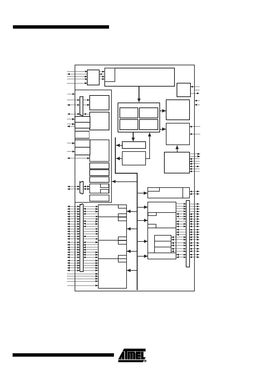
AT91 ARM
«
Thumb
«
-based
Microcontrollers
AT91SAM7S256
Summary
Preliminary
Note: This is a summary document. A complete document
is not available at this time. For more information, please
contact your local Atmel sales office.

2
AT91SAM7S256 Summary Preliminary
6117ASŁATARMŁ20-Oct-04
Ę
One Three-channel 16-bit Timer/Counter (TC)
Ł Three External Clock Inputs, Two Multi-purpose I/O Pins per Channel
Ł Double PWM Generation, Capture/Waveform Mode, Up/Down Capability
Ę
One Four-channel 16-bit PWM Controller (PWMC)
Ę
One Two-wire Interface (TWI)
Ł Master Mode Support Only, All Two-wire Atmel EEPROMs Supported
Ę
One 8-channel 10-bit Analog-to-Digital Converter, Four Channels Multiplexed with Digital I/Os
Ę
IEEE 1149.1 JTAG Boundary Scan on All Digital Pins
Ę
5V-tolerant I/Os, including Four High-current Drive I/O lines, Up to 16 mA Each
Ę
Power Supplies
Ł Embedded 1.8V Regulator, Drawing up to 100 mA for the Core and External Components
Ł 3.3V VDDIO I/O Lines Power Supply, Independent 3.3V VDDFLASH Flash Power Supply
Ł 1.8V VDDCORE Core Power Supply with Brownout Detector
Ę
Fully Static Operation: Up to 55 MHz at 1.65V and 85
░C Worst Case Conditions
Ę
Available in a 64-lead LQFP Package
Description
Atmel's AT91SAM7S256 is a member of a series of low pincount Flash microcontrollers
based on the 32-bit ARM RISC processor. It features a 256 Kbyte high-speed Flash and
a 64 Kbyte SRAM, a large set of peripherals, including a USB 2.0 device, and a com-
plete set of system functions minimizing the number of external components. The
device is an ideal migration path for 8-bit microcontroller users looking for additional per-
formance and extended memory.
The embedded Flash memory can be programmed in-system via the JTAG-ICE inter-
face or via a parallel interface on a production programmer prior to mounting. Built-in
lock bits and a security bit protect the firmware from accidental overwrite and preserves
its confidentiality.
The AT91SAM7S256 system controller includes a reset controller capable of managing
the power-on sequence of the microcontroller and the complete system. Correct device
operation can be monitored by a built-in brownout detector and a watchdog running off
an integrated RC oscillator.
The AT91SAM7S256 is a general-purpose microcontroller. Its integrated USB Device
port makes it an ideal device for peripheral applications requiring connectivity to a PC or
cellular phone. Its aggressive price point and high level of integration pushes its scope
of use far into the cost-sensitive, high-volume consumer market.