
1
Features
À
Low Power Consumption
À
Calendar from 1900 to 2099
À
Year 2000 Compliant
À
Programmable Periodic Interrupt Alarm Interrupt
À
AVR
«
User Interface Bus
À
Full Asynchronous Design
À
Full Scan Testable
À
Very Small Silicon Area
À
Test Vectors: at Least 93% Fault Coverage
À
Designed for Digital Keypad Applications (Parallel Load)
Description
The Real Time Clock (RTC) peripheral is designed for use with the AVR embedded
RISC core. It combines a complete time-of-day clock with alarm and a two-hundred
year Gregorian calendar, complemented by a programmable periodic interrupt. The
alarm and calendar registers are accessed by an 8-bit data bus.
The time and calendar values are coded in Binary-Coded Decimal (BCD) format. The
time format is 24-hour mode.
Updating time and calendar fields and configuring the alarm fields is performed by a
parallel capture on the 8-bit data bus. An entry control is performed to avoid loading
registers with incompatible BCD format data or with an incompatible date according to
the current month/year/century.
Year 2000 Conformity
The Real Time Clock Macrocell complies fully with the Year 2000 Conformity Require-
ments as stated in the British Standards Institution Document; Ref. BSI-DISC
PD2000-1: "Year 2000 conformity shall mean that neither performance nor functional-
ity is affected by dates prior to, during and after the year 2000".
It has been tested to be compliant with the four associated rules:
1.
No value for current date will cause any interruption in operation.
2.
Date-based functionality must behave consistently for dates prior to, during and
after year 2000.
3.
In all interfaces and data storage, the century in any date must be specified either
explicitly or by unambiguous algorithms or inferencing rules.
4.
Year 2000 must be recognized as a leap year.
The RTC represents the year as a four-digit number (..., 1998, 1999, 2000, 2001, etc.)
so that the century is unambiguously identified, in accordance with Rule 3.
Scan Test Configuration
The fault coverage is maximum if all non-scan inputs can be controlled and all non-
scan outputs can be observed. In order to achieve this, the ATPG vectors must be
generated on the entire circuit (top level) which includes the RTC or all RTC I/Os must
have a top level access and ATPG vectors must be applied to these pins.
Higher fault coverage may be achieved by applying manual vectors to the 32768
divider.
Embedded RISC
Microcontroller
Core Peripheral
Real Time Clock
(RTC)
Rev. 1302B¡07/01
2
RTC
1302B¡07/01
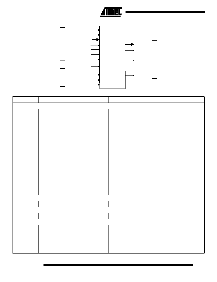
Figure 1. RTC Pin Configuration
Table 1. Pin Description
Pin Name
Description
Direction
Comments
AVR Control
cp2
CPU clock
Input
Any register in the RTC will update its contents only on the
positive edge of cp2.
ireset
Synchronous reset
Input
When high, ireset will reset internal registers by reading the value
on dbus_in which is forced to zero by the AVR Core.
dbus_in[7:0]
Data bus input
Input
dbus_out[7:0]
Data bus output
Output
Valid only when out_en is high.
out_en
Output enable strobe
Output
When high, out_en indicates that the RTC requires control of the
data bus.
cs
Chip Select
Input
When high, adr, iore and iowe are used to access internal RTC
I/Os. When low, the RTC cannot be accessed in either read or
write mode.
adr
I/O address input
Input
Connects to LSB of AVR adr[5:0] bus. Valid only when
accompanied by a strobe on iore or iowe.
iore
I/O read strobe
Input
Used to read the contents of the I/O location addressed by adr.
Active high.
iowe
I/O write strobe
Input
Used to update the contents of the I/O location addressed by adr.
Active high.
RTC
clk32768
Main clock for RTC
Input
F = 32.768 kHz (Crystal oscillator).
IRQ
rtc_int
Interrupt
Output
Programmable from alarm and/or event. Active high.
Scan Test
test_mode
Clock selection for test
purposes
Input
All flip-flops are driven with the same clock (clk32768). Active
high/low.
test_si
Test scan inputs
Input
Input of scan chain.
test_so
Test scan outputs
Output
Output of scan chain.
test_se
Test scan enable
Input
Scan shift/scan capture.
adr
dbus_in[7:0]
iore
iowe
clk32768
cp2
test_mode
out_en
test_so
RTC
AVR Control
AVR Control
test_se
test_si
Scan Test
Scan Test
ireset
dbus_out[7:0]
RTC
rtc_int
IRQ
cs

3
RTC
1302B¡07/01
Functional
Description
The RTC provides a full Binary-Coded Decimal (BCD) clock which includes century (19/20),
year (with leap years), month, date, day, hours, minutes and seconds.
The valid year range is 1900 to 2099, a two-hundred year Gregorian calendar achieving full
Y2K compliance.
The RTC operates in 24-hour mode.
Corrections for leap years are included (all years divisible by 4 being leap years, including
year 2000). This is correct up to the year 2099.
RTC Chip Select
(cs)
The RTC has the ability to be remapped inside the AVR I/O address range. A small amount of
glue logic must be inserted to generate the cs signal. To access the internal I/O locations of
the RTC, the following condition must be true:
cs = 1
Under this condition, iore, iowe and adr are used to access the internal RTC I/O for reading or
writing. The cs input is generated from the decoding of the five AVR adr MSBs. To obtain the
Base Address (BaseAdr) for RTC addressing, use the following logic:
cs = (adr[5:1] = = cs_adr[4:0])
Where the value of cs_adr is assigned by the designer; the binary value {cs_adr[4:0], 0} is the
Base Address (BaseAdr) for RTC addressing.
The BaseAdr and corresponding restrictions for each value of cs_adr are shown in Table 2.
The 1-bit adr provides the offset which locates the RTC registers, as shown in Table 3..
Table 2. cs_adr/BaseAdr
cs_adr
BaseAdr
Comment
0x00
0x01
.
.
.
.
0x0F
0x10
.
.
.
0x1b
0x1c
.
.
.
0x1F
0x00
0x02
.
.
.
.
0x1E
0x20
.
.
.
0x36
0x38
.
.
.
0x3E
Allowed
¡
.
.
.
.
¡
¡
.
.
.
¡
Not Allowed
.
.
.
Not Allowed
Table 3. RTC Address/Data Registers
adr
RTC Register
0
RTC Internal Address Register
1
RTC Internal Data Register

4
RTC
1302B¡07/01
Timing
The RTC is updated in real time at one second intervals in normal mode for the seconds
counter, at 1 minute intervals for the minutes counter and so on.
Due to the asynchronous operation of the RTC with respect to the rest of the chip, to be cer-
tain that the values read in the RTC registers (century, year, month, date, day, hours, minutes,
seconds) are valid and stable, it is necessary to read these registers twice. If the data is the
same both times, then it is valid. Therefore, a minimum of two and a maximum of three
accesses is required.
Alarm
The RTC has four programmable fields: date, hours, minutes and seconds. Each of these
fields can be enabled or disabled to match the alarm condition.
À
If all the fields are enabled, an alarm flag is generated (the corresponding flag is asserted
and an interrupt generated if enabled) at a given date/hour/minute/second.
À
If only the seconds field is enabled, then an alarm is generated every minute.
À
Depending on the combination of fields enabled, a large number of possibilities are
available to the user ranging from minutes to 365/366 days.
Error Checking
A verification of user interface data is performed when accessing the century, year, month,
date, day, hours, minutes, seconds and alarms. A check is performed for illegal BCD entries
such as illegal date of the month with regards to the year and century configured.
If one of the time fields is not correct, the data is not loaded into the register/counter and a flag
is set in the validity register. This flag cannot be reset by the user. It is reset as soon as an
acceptable value is programmed. This avoids any further side effects in the hardware. The
same procedure is done for the alarm.
The following checks are performed:
1.
Century (check if it is in range 19-20)
2.
Year (BCD entry check)
3.
Date (check range 01-31)
4.
Month (check if it is in BCD range 01-12, check validity regarding "date")
5.
The order of the following steps can be random.
6.
Day (check range 1-7)
7.
Hour (BCD check, check range 00-23)
8.
Minute (check BCD and range 00-59)
9.
Second (check BCD and range 00-59)
Updating
Time/Calendar
To update any of the time/calendar fields, the user must first stop the RTC by setting the corre-
sponding field in the Control Register (RTC_CR). Bit UPDTIM must be set to update time
fields (hour, minute, second) and bit UPDCAL must be set to update calendar fields (century,
year, month, date, day).
Then the user must poll or wait for the interrupt (if enabled) of bit ACKUPD in the Status Reg-
ister. Once the bit reads 1, the user can write to the appropriate register.
Once the update is finished, the user must reset (0) UPDTIM and/or UPDCAL in the control
register.
When programming the calendar fields, the time fields remain enabled. This avoids a time slip
in case the user stays in the calendar update phase for several tens of seconds or more.
5
RTC
1302B¡07/01
Read/Write Access
from the AVR
Only two registers can be directly accessed by the user:
À
The Internal Address Register (BaseAdr+0) stores the offset of the targeted RTC register
À
The Internal Data Register (BaseAdr+1) loads the data to the dedicated RTC register
identified by the offset.
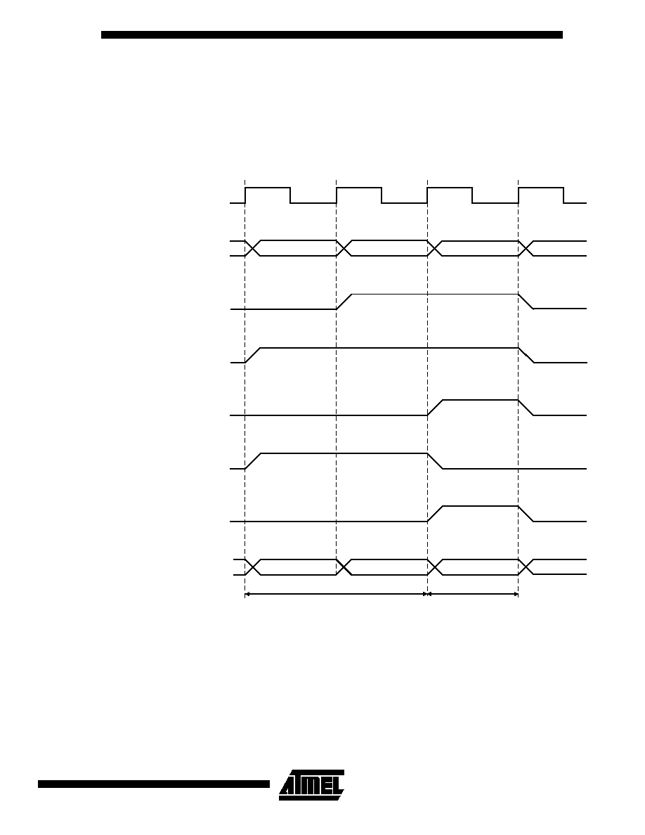
Timing Diagram
Figure 2. RTC Write Cycle
cp2
iowe
adr
iore
dbus_in
dbus_out
X
FF
0x00 (offset)
0xFF (data)
X
X
X
X
out_en
write cycle
read cycle
(from same
address as write)
cs