Note: This is a summary document. A complete document is
available under NDA. For more information, please contact your
local Atmel sales office.
Features
∑
Secure Computation of Public Key Signatures
∑
Secure Storage and Decryption of Symmetric Keys
∑
On-chip Cache for Frequently Used Keys
∑
SMBus Communications Port
∑
On-board Public Key Computation Engine and Microprocessor
∑
Physical and Logical Security Measures to Inhibit Attacks
∑
20-lead SOIC Package, 0
įC to +70įC Operating Range
∑
3.3V Ī10% Supply Voltage
Description
The AT90SP0801 is used to perform cryptographic operations, using asymmetric pri-
vate keys stored in its internal EEPROM. An arbitrary number of private keys can be
stored externally and decrypted by the chip when required. Communication to the sys-
tem processor is via the SMBus.
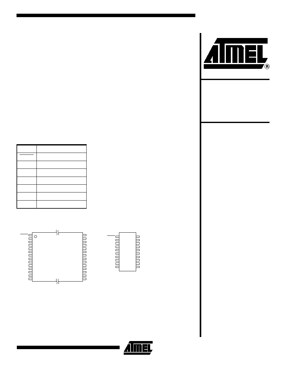
Figure 1. Pin Configuration
Name
Description
RESET
Reset Input, Active-low
SCL
SMBus Clock
SDA
SMBus Data
GND
Ground
CLKIN
Input Clock
VCC
Operating Voltage
TEST
Do Not Connect
1
2
3
4
5
6
7
8
9
10
11
12
13
14
RESET
NC
NC
NC
NC
NC
SCL
SDA
NC
NC
NC
GND
NC
NC
28
27
26
25
24
23
22
21
20
19
18
17
16
15
NC
NC
VCC
NC
NC
NC
NC
NC
CLKIN
TEST
TEST
NC
NC
NC
1
2
3
4
5
6
7
8
9
10
20
19
18
17
16
15
14
13
12
11
RESET
NC
NC
NC
NC
SCL
SDA
NC
NC
GND
VCC
NC
NC
NC
NC
CLKIN
TEST
NC
NC
TEST
28-lead TSSOP
28-lead SOIC
Secure
Signature
Generation Chip
AT90SP0801
Summary
Rev. 1495AS≠01/02

2
AT90SP0801
1495AS≠01/02
Figure 2. Block Diagram
I/O Buffer
8/16-bit
AVR
Ķp
Program
Memory
Crypto Data
Buffer
Public Key
Crypto
Engine
Hardware Key
Private Key
Password
EEPROM
Registers
User Key Buffer 0
Private Key
Password, Mode
CRC Tag
User Key Buffer 1
Private Key
Password, Mode
CRC Tag
Other Configuration
Registers:
LOCK, STATUS
ERROR, VERS
FAILCNT, CONFIG
Commands
Data
SMBus
Control:
Data:
CLKIN
RESET
Key:
3
AT90SP0801
1495AS≠01/02
Serial Interface
Data is transferred to or from the I/O buffer on the chip using the SMBus interface, in a
manner similar but not identical to that of standard two-wire serial EEPROMs.
All bits are sent to or read from the chip most significant bit first, in a manner consistent
with standard serial EEPROMs. Bit fields listed in this document are correspondingly
listed with the MSB on the left and the LSB on the right. Hex numbers are specified with
the "0x" prefix.
Multi-byte information sent to the chip is sent most significant byte first, following typical
conventions. Within the chip, the first byte sent to the chip is stored in memory at the
lowest address, and the address is incremented for subsequent bytes. When a mes-
sage digest (hash) is sent to the chip, the first byte of the hash value is the first byte to
be sent to the chip.
In both the text and graphics, the chip is the slave and the system is the master. The fol-
lowing abbreviations apply:
For the graphical representations, the direction of the data flow is indicated as below:
SMBus Standard Usage
Data transfer to and from the chip follows the SMBus V1.1 standard, using only some of
the command protocols.
The "write" command of this chip uses the "Block Write" protocol of the SMBus spec.
Note that in this chip the count value can exceed 32. This chip does not support the
"Write Byte" and "Write Word" protocols of the SMBus spec.
The "Read" command of this chip uses the "Block Read" protocol of the SMBus spec.
Note that in this chip the "Read" command can be optionally executed without the pre-
ceding partial block write command. This chip does not support the "Receive Byte",
"Read Byte" and "Read Word" protocols of the SMBus spec.
All other commands of this chip use the "Send Byte" protocol of the SMBus spec. Note
that the "Quick Command" and "Process Call" protocols of the SMBus spec are not sup-
ported by this chip.
Two-wire Serial EEPROM
Comparison
Some of the differences between this chip and a standard two-wire serial EEPROM are:
1.
The slave address of this chip is different from the A0-AF (hex) standard for
EEPROMs.
2.
The maximum clock rate is 100 kHz and Tdh is 300 ns. These specs are part of
SMbus.
3.
The supply voltage is 3.0V to 3.7V.
4.
The read address is not specified in the aborted read command.
5.
Multi-byte reads and writes are preceded by the number of bytes that will be
transferred.
A
Acknowledge (bus pulled low, master or slave)
N
Not Acknowledge (bus left high, master or slave)
S
Start (High-to-low on SDA with SCL high, master)
P
Stop (Low-to-high on SDA with SCL high, master)
Slave to Master
(Chip to System)
Master to Slave
(System to Chip)
4
AT90SP0801
1495AS≠01/02
6.
Multi-byte writes longer than the maximum size of the register (i.e., containing
more bytes) cause an error.
Commands Without Data
Transfer
There are a number of commands (described within the following Commands sections)
that perform various internal operations on the chip, using data already stored in either
the I/O buffer or the internal memories of the chip. All such commands are composed of
two bytes sent to the chip according to the following flow:
Write Commands
The write commands permit data to be transferred to the I/O buffer located within the
SRAM on the chip. Only block writes are supported, so transfers of 1 or 2 bytes require
the same basic sequence as 32 bytes.
The commands are encoded as follows:
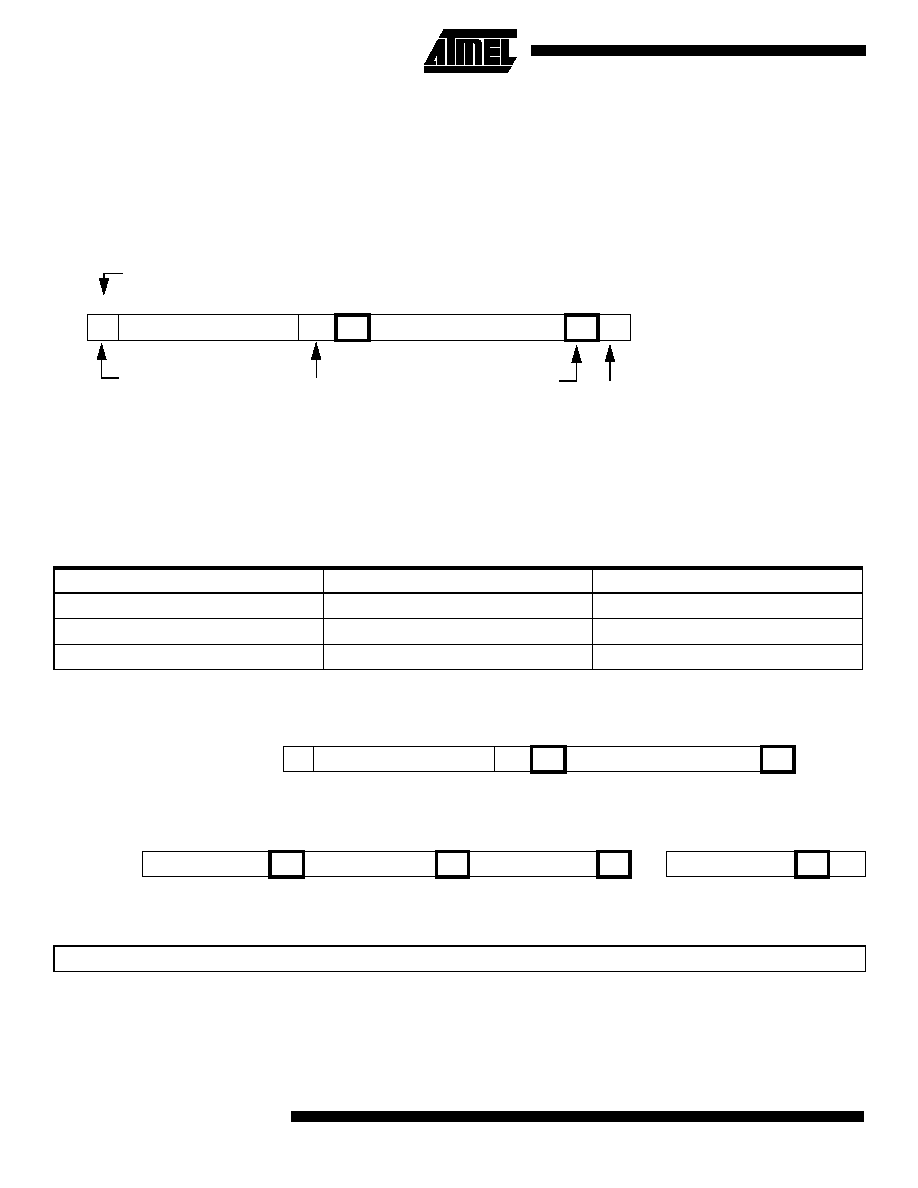
The following figure shows the structure for block write operations:
The write buffer command is followed by up to 255 bytes of data. All bytes are sourced
by the host and are formatted as follows:
Count denotes the total number of bytes that follows the command, including any CRC
bytes. A 0 value is illegal. 255 is the max. number of bytes that may be written per
command.
S
Slave Address
Wr
A
Command Code
A
P
Start Condition
R/W Bit
Acknowledge
Stop Condition
1
7
1
1
8
1
1
Number of bits
Slave Address
Command Code
Description
0 1 0 1 0 0 0 0
s
1
s
0
0 0 0 0 0 0
Write buffer, (+data)
0 1 0 1 0 0 1 0
0 1 1 1 1 1 1 1
Write command, ignored
0 1 0 1 0 0 0 0
0 1 1 1 1 1 1 1
Write command, ignored
1
7
1
1
8
1
...
S
Slave Address
Wr
A
Command Code
A
8
1
8
1
8
1
...
8
1
1
Byte Count = N
A
Data byte 1
A
Data byte 2
A
Data byte N
A
P
01010000
s
1
s
0
000000
count
data0
data1
...
dataN
crc0
crc1

5
AT90SP0801
1495AS≠01/02
Data is sent least significant byte first. In some circumstances, there may be no data,
only crc.
Depending on the value of ss, the crc bytes may or may not be included.
The two sequence bits s
1-0
within the command code tell the chip how to relate this
transfer to previous and subsequent transfers.
S
0
if set to a 1 indicates that this is the first transfer to the buffer and that data0 should
go into buffer address 0 and so on. If this bit is set to a 0, then data0 will be stored in the
next location within the buffer after that from the previous transfer. When set, this bit
also resets the CRC generator.
S
1
if set to a 1 indicates that this is the last transfer to the buffer. If set to a 0, the chip
must have previously executed a command where s
0
was set to a 1. When s
1
is set to a
1, the last two bytes of the information transferred in this block are a CRC value. The
chip will NACK the crc1 byte, if the value sent does not match that computed on the
incoming data. The CRC bytes may not be split across two blocks.
For instance, to write password information (64 bytes) to the chip, the following
sequence of three write commands would be used (assuming 32 byte loads). The
ACKs, NACKs and STOP conditions have been ignored for clarity.
For shorter data transfer values, it is perfectly legal for both s
0
and s
1
to be set. This indi-
cates that the entire transfer is taking place in a single block access. As an example of
this, the following command would write a single byte to the buffer:
The chip will NACK writes that attempt to write into the chip beyond the internal buffer,
which may be as short as 320 bytes.
S
01010000
01000000
00100000
data0
data1
data2
...
data31
S
01010000
00000000
00100000
data32
data33
data34
...
data63
S
01010000
10000000
00000010
crc0
crc1
S
01010000
11000000
00000011
data0
crc0
crc1