1
Features
·
Utilizes the AVR
®
RISC Architecture
·
AVR High-performance and Low-power RISC Architecture
89 Powerful Instructions Most Single Clock Cycle Execution
32 x 8 General Purpose Working Registers
Up to 12 MIPS Throughput at 12 MHz
·
Data and Non-volatile Program Memory
1K Byte of In-System Programmable Flash
Endurance: 1,000 Write/Erase Cycles
64 Bytes of In-System Programmable EEPROM
Endurance: 100,000 Write/Erase Cycles
Programming Lock for Flash Program and EEPROM Data Security
·
Peripheral Features
One 8-bit Timer/Counter with Separate Prescaler
On-chip Analog Comparator
Programmable Watchdog Timer with On-chip Oscillator
SPI Serial Interface for In-System Programming
·
Special Microcontroller Features
Low-power Idle and Power-down Modes
External and Internal Interrupt Sources
Selectable On-chip RC Oscillator for Zero External Components
·
Specifications
Low-power, High-speed CMOS Process Technology
Fully Static Operation
·
Power Consumption at 4 MHz, 3V, 25
°C
Active: 2.0 mA
Idle Mode: 0.4 mA
Power-down Mode: <1 µA
·
I/O and Packages
15 Programmable I/O Lines
20-pin PDIP, SOIC and SSOP
·
Operating Voltages
2.7 - 6.0V (AT90S1200-4)
4.0 - 6.0V (AT90S1200-12)
·
Speed Grades
0 - 4 MHz, (AT90S1200-4)
0 - 12 MHz, (AT90S1200-12)
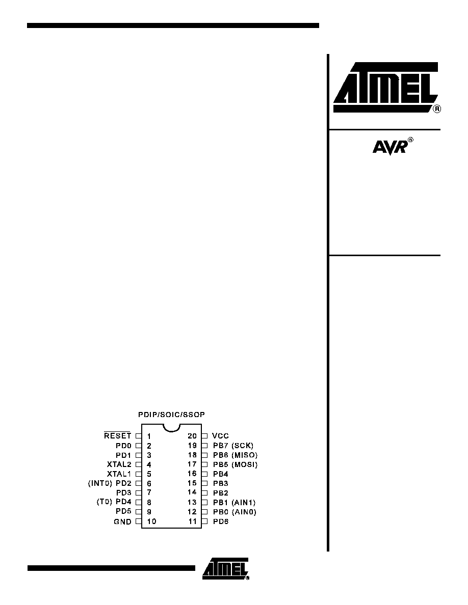
Pin Configuration
8-bit
Microcontroller
with 1K Byte
of In-System
Programmable
Flash
AT90S1200
Summary
Rev. 0838HSAVR03/02
Note: This is a summary document. A complete document is
available on our web site at
www.atmel.com
.
2
AT90S1200
0838HSAVR03/02
Description
The AT90S1200 is a low-power CMOS 8-bit microcontroller based on the AVR RISC
architecture. By executing powerful instructions in a single clock cycle, the AT90S1200
achieves throughputs approaching 1 MIPS per MHz allowing the system designer to
optimize power consumption versus processing speed.
The AVR core combines a rich instruction set with the 32 general purpose working reg-
isters. All the 32 registers are directly connected to the Arithmetic Logic Unit (ALU),
allowing two independent registers to be accessed in one single instruction executed in
one clock cycle. The resulting architecture is more code efficient while achieving
throughputs up to ten times faster than conventional CISC microcontrollers.
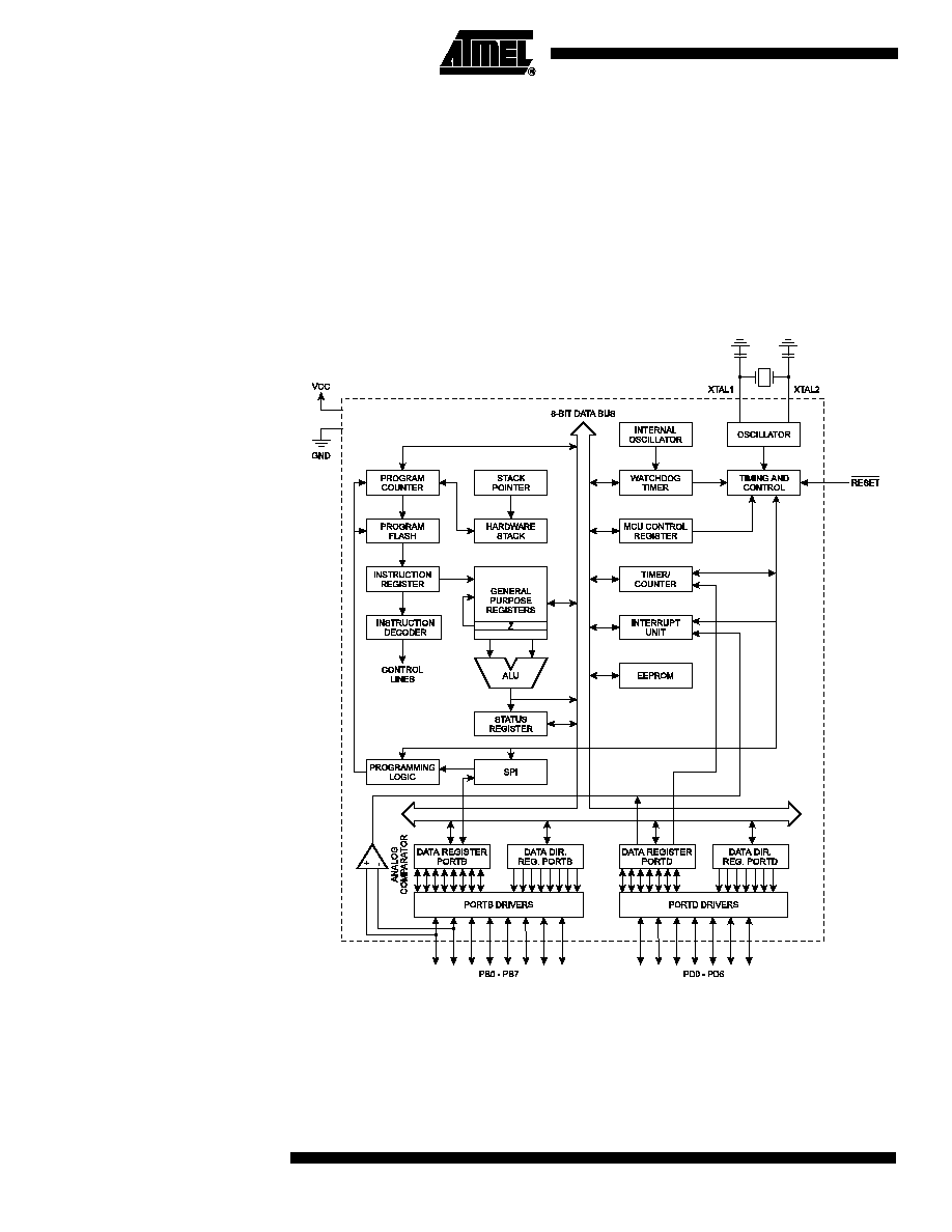
Block Diagram
Figure 1. The AT90S1200 Block Diagram
The architecture supports high-level languages efficiently as well as extremely dense
assembler code programs. The AT90S1200 provides the following features: 1K byte of
In-System Programmable Flash, 64 bytes EEPROM, 15 general purpose I/O lines, 32
general purpose working registers, internal and external interrupts, programmable
watchdog timer with internal oscillator, an SPI serial port for program downloading and
two software selectable power-saving modes. The Idle Mode stops the CPU while allow-

3
AT90S1200
0838HSAVR03/02
ing the Registers, Timer/Counter, Watchdog and Interrupt system to continue
functioning. The Power-down mode saves the register contents but freezes the Oscilla-
tor, disabling all other chip functions until the next External Interrupt or hardware Reset.
The device is manufactured using Atmel's high-density nonvolatile memory technology.
The On-chip In-System Programmable Flash allows the program memory to be repro-
grammed in-system through an SPI serial interface or by a conventional nonvolatile
memory programmer. By combining an enhanced RISC 8-bit CPU with In-System Pro-
g ram m abl e F la sh on a mo nol ithi c chi p, th e Atme l AT 90S1 200 is a p ower fu l
microcontroller that provides a highly flexible and cost-effective solution to many embed-
ded control applications.
The AT90S1200 AVR is supported with a full suite of program and system development
tools including: macro assemblers, program debugger/simulators, in-circuit emulators,
and evaluation kits.
Pin Descriptions
VCC
Supply voltage pin.
GND
Ground pin.
Port B (PB7..PB0)
Port B is an 8-bit bi-directional I/O port. Port pins can provide internal pull-up resistors
(selected for each bit). PB0 and PB1 also serve as the positive input (AIN0) and the
negative input (AIN1), respectively, of the On-chip Analog Comparator. The Port B out-
put buffers can sink 20 mA and thus drive LED displays directly. When pins PB0 to PB7
are used as inputs and are externally pulled low, they will source current if the internal
pull-up resistors are activated. The Port B pins are tri-stated when a reset condition
becomes active, even if the clock is not active.
Port B also serves the functions of various special features of the AT90S1200 as listed
on page 30.
Port D (PD6..PD0)
Port D has seven bi-directional I/O pins with internal pull-up resistors, PD6..PD0. The
Port D output buffers can sink 20 mA. As inputs, Port D pins that are externally pulled
low will source current if the pull-up resistors are activated. The Port D pins are tri-stated
when a reset condition becomes active, even if the clock is not active.
Port D also serves the functions of various special features of the AT90S1200 as listed
on page 34.
RESET
Reset input. A low level on this pin for more than 50 ns will generate a reset, even if the
clock is not running. Shorter pulses are not guaranteed to generate a reset.
XTAL1
Input to the inverting oscillator amplifier and input to the internal clock operating circuit.
XTAL2
Output from the inverting oscillator amplifier.
4
AT90S1200
0838HSAVR03/02
Notes:
1. For compatibility with future devices, reserved bits should be written to zero if accessed. Reserved I/O memory addresses
should never be written.
2. Some of the status flags are cleared by writing a logical "1" to them. Note that the CBI and SBI instructions will operate on all
bits in the I/O register, writing a "1" back into any flag read as set, thus clearing the flag. The CBI and SBI instructions work
with registers $00 to $1F only.
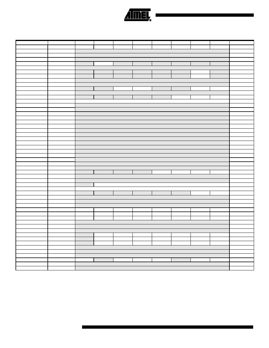
AT90S1200 Register Summary
Address
Name
Bit 7
Bit 6
Bit 5
Bit 4
Bit 3
Bit 2
Bit 1
Bit 0
Page
$3F
SREG
I
T
H
S
V
N
Z
C
page 11
$3E
Reserved
$3D
Reserved
$3C
Reserved
$3B
GIMSK
-
INT0
-
-
-
-
-
-
page 15
$3A
Reserved
$39
TIMSK
-
-
-
-
-
-
TOIE0
-
page 16
$38
TIFR
-
-
-
-
-
-
TOV0
-
page 16
$37
Reserved
$36
Reserved
$35
MCUCR
-
-
SE
SM
-
-
ISC01
ISC00
page 18
$34
Reserved
$33
TCCR0
-
-
-
-
-
CS02
CS01
CS00
page 21
$32
TCNT0
Timer/Counter0 (8 Bits)
page 22
$31
Reserved
$30
Reserved
$2F
Reserved
$2E
Reserved
$2D
Reserved
$2C
Reserved
$2B
Reserved
$2A
Reserved
$29
Reserved
$28
Reserved
$27
Reserved
$26
Reserved
$25
Reserved
$24
Reserved
$23
Reserved
$22
Reserved
$21
WDTCR
-
-
-
-
WDE
WDP2
WDP1
WDP0
page 23
$20
Reserved
$1F
Reserved
$1E
EEAR
-
EEPROM Address Register
page 25
$1D
EEDR
EEPROM Data Register
page 25
$1C
EECR
-
-
-
-
-
-
EEWE
EERE
page 25
$1B
Reserved
$1A
Reserved
$19
Reserved
$18
PORTB
PORTB7
PORTB6
PORTB5
PORTB4
PORTB3
PORTB2
PORTB1
PORTB0
page 29
$17
DDRB
DDB7
DDB6
DDB5
DDB4
DDB3
DDB2
DDB1
DDB0
page 29
$16
PINB
PINB7
PINB6
PINB5
PINB4
PINB3
PINB2
PINB1
PINB0
page 29
$15
Reserved
$14
Reserved
$13
Reserved
$12
PORTD
-
PORTD6
PORTD5
PORTD4
PORTD3
PORTD2
PORTD1
PORTD0
page 34
$11
DDRD
-
DDD6
DDD5
DDD4
DDD3
DDD2
DDD1
DDD0
page 34
$10
PIND
-
PIND6
PIND5
PIND4
PIND3
PIND2
PIND1
PIND0
page 34
$0F
Reserved
...
Reserved
$09
Reserved
$08
ACSR
ACD
-
ACO
ACI
ACIE
-
ACIS1
ACIS0
page 27
...
Reserved
$00
Reserved

5
AT90S1200
0838HSAVR03/02
Instruction Set Summary
Mnemonic
Operands
Description
Operation
Flags
# Clocks
ARITHMETIC AND LOGIC INSTRUCTIONS
ADD
Rd, Rr
Add Two Registers
Rd
Rd + Rr
Z,C,N,V,H
1
ADC
Rd, Rr
Add with Carry Two Registers
Rd
Rd + Rr + C
Z,C,N,V,H
1
SUB
Rd, Rr
Subtract Two Registers
Rd
Rd - Rr
Z,C,N,V,H
1
SUBI
Rd, K
Subtract Constant from Register
Rd
Rd - K
Z,C,N,V,H
1
SBC
Rd, Rr
Subtract with Carry Two Registers
Rd
Rd - Rr - C
Z,C,N,V,H
1
SBCI
Rd, K
Subtract with Carry Constant from Reg.
Rd
Rd - K - C
Z,C,N,V,H
1
AND
Rd, Rr
Logical AND Registers
Rd
Rd
·
Rr
Z,N,V
1
ANDI
Rd, K
Logical AND Register and Constant
Rd
Rd
·
K
Z,N,V
1
OR
Rd, Rr
Logical OR Registers
Rd
Rd v Rr
Z,N,V
1
ORI
Rd, K
Logical OR Register and Constant
Rd
Rd v K
Z,N,V
1
EOR
Rd, Rr
Exclusive OR Registers
Rd
Rd
Rr
Z,N,V
1
COM
Rd
One's Complement
Rd
$FF - Rd
Z,C,N,V
1
NEG
Rd
Two's Complement
Rd
$00 - Rd
Z,C,N,V,H
1
SBR
Rd, K
Set Bit(s) in Register
Rd
Rd v K
Z,N,V
1
CBR
Rd, K
Clear Bit(s) in Register
Rd
Rd
·
(FFh - K)
Z,N,V
1
INC
Rd
Increment
Rd
Rd + 1
Z,N,V
1
DEC
Rd
Decrement
Rd
Rd - 1
Z,N,V
1
TST
Rd
Test for Zero or Minus
Rd
Rd
·
Rd
Z,N,V
1
CLR
Rd
Clear Register
Rd
Rd
Rd
Z,N,V
1
SER
Rd
Set Register
Rd
$FF
None
1
BRANCH INSTRUCTIONS
RJMP
k
Relative Jump
PC
PC + k + 1
None
2
RCALL
k
Relative Subroutine Call
PC
PC + k + 1
None
3
RET
Subroutine Return
PC
STACK
None
4
RETI
Interrupt Return
PC
STACK
I
4
CPSE
Rd, Rr
Compare, Skip if Equal
if (Rd = Rr) PC
PC + 2 or 3
None
1/2
CP
Rd, Rr
Compare
Rd - Rr
Z,N,V,C,H
1
CPC
Rd, Rr
Compare with Carry
Rd - Rr - C
Z,N,V,C,H
1
CPI
Rd, K
Compare Register with Immediate
Rd - K
Z,N,V,C,H
1
SBRC
Rr, b
Skip if Bit in Register Cleared
if (Rr(b) = 0) PC
PC + 2 or 3
None
1/2
SBRS
Rr, b
Skip if Bit in Register is Set
if (Rr(b) = 1) PC
PC + 2 or 3
None
1/2
SBIC
P, b
Skip if Bit in I/O Register Cleared
if (P(b)= 0) PC
PC + 2 or 3
None
1/2
SBIS
P, b
Skip if Bit in I/O Register is Set
if (P(b) = 1) PC
PC + 2 or 3
None
1/2
BRBS
s, k
Branch if Status Flag Set
if (SREG(s) = 1) then PC
PC + k + 1
None
1/2
BRBC
s, k
Branch if Status Flag Cleared
if (SREG(s) = 0) then PC
PC + k + 1
None
1/2
BREQ
k
Branch if Equal
if (Z = 1) then PC
PC + k + 1
None
1/2
BRNE
k
Branch if Not Equal
if (Z = 0) then PC
PC + k + 1
None
1/2
BRCS
k
Branch if Carry Set
if (C = 1) then PC
PC + k + 1
None
1/2
BRCC
k
Branch if Carry Cleared
if (C = 0) then PC
PC + k + 1
None
1/2
BRSH
k
Branch if Same or Higher
if (C = 0) then PC
PC + k + 1
None
1/2
BRLO
k
Branch if Lower
if (C = 1) then PC
PC + k + 1
None
1/2
BRMI
k
Branch if Minus
if (N = 1) then PC
PC + k + 1
None
1/2
BRPL
k
Branch if Plus
if (N = 0) then PC
PC + k + 1
None
1/2
BRGE
k
Branch if Greater or Equal, Signed
if (N
V = 0) then PC
PC + k + 1
None
1/2
BRLT
k
Branch if Less than Zero, Signed
if (N
V = 1) then PC
PC + k + 1
None
1/2
BRHS
k
Branch if Half-carry Flag Set
if (H = 1) then PC
PC + k + 1
None
1/2
BRHC
k
Branch if Half-carry Flag Cleared
if (H = 0) then PC
PC + k + 1
None
1/2
BRTS
k
Branch if T-Flag Set
if (T = 1) then PC
PC + k + 1
None
1/2
BRTC
k
Branch if T-Flag Cleared
if (T = 0) then PC
PC + k + 1
None
1/2
BRVS
k
Branch if Overflow Flag is Set
if (V = 1) then PC
PC + k + 1
None
1/2
BRVC
k
Branch if Overflow Flag is Cleared
if (V = 0) then PC
PC + k + 1
None
1/2
BRIE
k
Branch if Interrupt Enabled
if (I = 1) then PC
PC + k + 1
None
1/2
BRID
k
Branch if Interrupt Disabled
if (I = 0) then PC
PC + k + 1
None
1/2
DATA TRANSFER INSTRUCTIONS
LD
Rd, Z
Load Register Indirect
Rd
(Z)
None
2
ST
Z, Rr
Store Register Indirect
(Z)
Rr
None
2
MOV
Rd, Rr
Move between Registers
Rd
Rr
None
1
LDI
Rd, K
Load Immediate
Rd
K
None
1
IN
Rd, P
In Port
Rd
P
None
1
OUT
P, Rr
Out Port
P
Rr
None
1