
5033ASWIRE10/03
Features
·
850930 MHz Output Frequency
·
Rx Current: 14.5 mA
·
Low Sleep Mode Current: 1 uA
·
DSSS Processing and BPSK Modulation/Demodulation
·
Battery Voltage Monitoring Circuitry
·
4 mW (6 dBm) Min. Transmit Power @ Vdd = 1.8V
·
Serial Peripheral Interface (SPI) Control
·
Power Supply Voltage Operating Range: 1.8V to 3.6V
·
Low External Component Count
·
48QFN Package
Applications
·
Low Band IEEE 802.15.4/ZigBee
TM
-based Systems
·
Industrial, Commercial, Home Lighting Control, Security, and HVAC
·
Inventory Management
·
Health Monitoring
·
Wireless PC Peripherals such as Mouse, Keyboard, and Joystick
·
Consumer Electronics Remote Controls and Toys
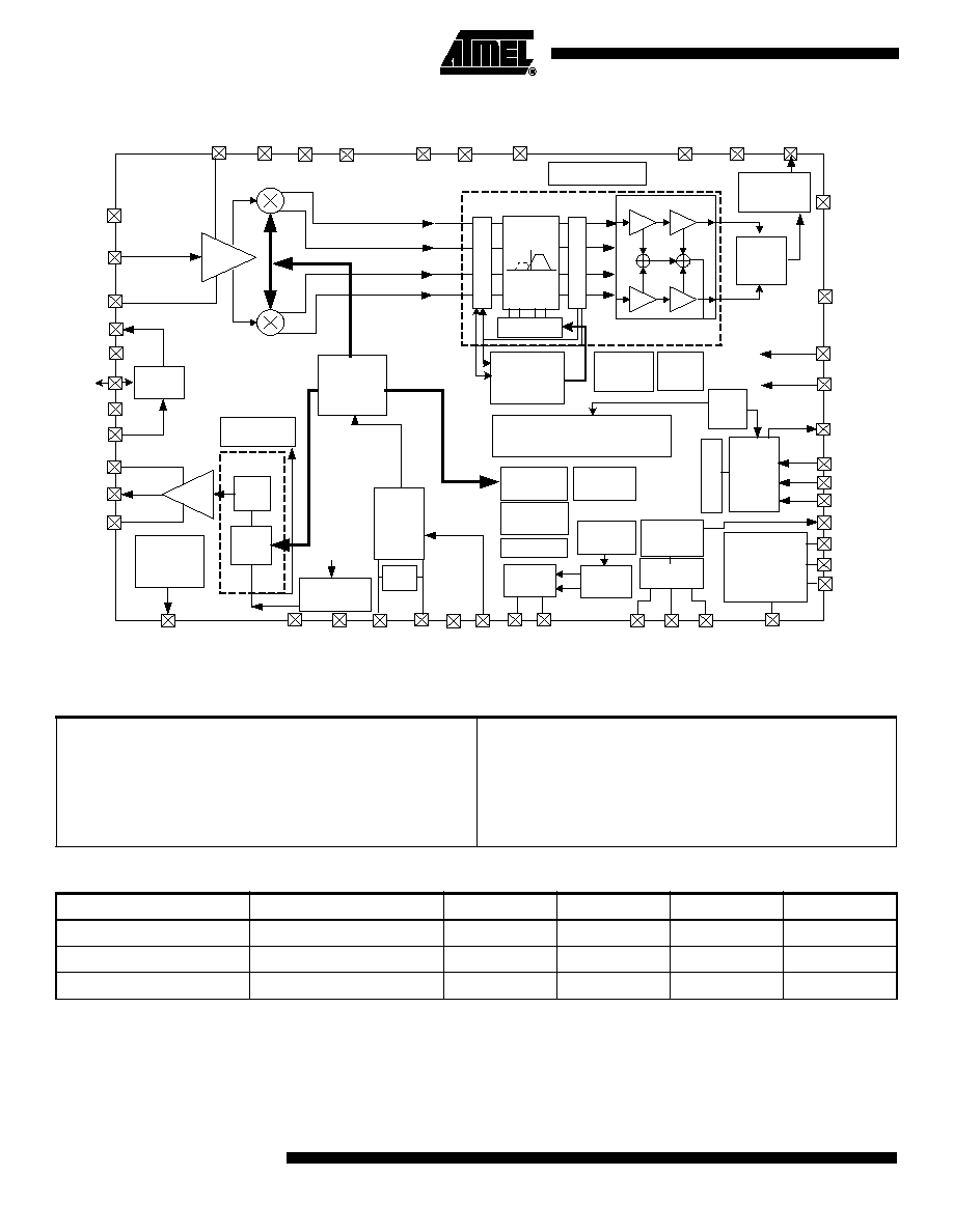
Description
The Atmel AT86RF210 Z-Link
TM
Transceiver is a fully integated, low-cost ZigBee
TM
transceiver capable of transmitting and receiving BPSK modulated digital data over a
frequency range of 868 MHz and 902928 MHz using a minimum number of external
components. It combines excellent RF performance with low cost, small size and low
current consumption. The AT86RF210 includes a crystal stabilized Fractional-N syn-
thesizer, BPSK transmitter and receiver, and full Direct Sequence Spread Spectrum
Signal (DSSS) processing, including spreading and despreading. The device is fully
compatable with IEEE 802.15.4 and ZigBee standards. It includes internal voltage
regulation and battery monitoring circuitry and requires a minimum number of external
support components.
Figure 1. Block Diagram
SEL
X
Synthesizer
Modulator
Polyphase
Filter
Power Amp
Low Noise
Amp
I/Q Mixer
IF Amp
Demodulator
Despreader
SPI Bus
Spreader
T/R Switch
Rx In
Tx Out
Data In
Data Out
Sw In
Sw Out
Ant In
SDI
SDO
SCLK
AT86RF210
Z-Link
TM
Transceiver
868/902928 MHz
Direct Sequence
Spread Spectrum
BPSK Transceiver
Preliminary
2
AT86RF210
5033ASWIRE10/03
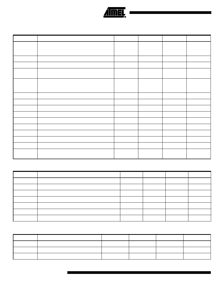
Figure 1. Functional Block Diagram
Note:
Unit operation is guaranteed by design when operating within these ranges.
Table 1. Absolute Maximum Ratings*
Storage Temperature ..............................................
-
65 to +150
*NOTE: Stresses beyond those listed in this table may cause per-
manent damage to the device. This is a stress rating
only; functional operation of the device at these or any
other conditions beyond those indicated in the opera-
tion al sections of the specification is not implied.
Exposure to the absolute maximum rating conditions for
extended periods may affect device reliability.
Maximum Input Voltage...........................................VDD + 0.5V
Maximum Operating Voltage (VDD ) ................................... 4,5
Table 2. Operating Conditions
Symbol
Parameter
Min
Typ
Max
Unit
TAMB
Operating temperature
-
40
85
°C
VSUPPLY
Voltage supply range
1.8
2.7
3.6
V
HUMIDITY
Humidity
10
90
%
LNAVSS
VSS
RSWOUT
LNAIN
ANT
Image
Reject
Filter
LNA
VCO
TUNE
GND
LNAOUT
IQ-Limiter Strip
1.2 MHz
SDI
SDO
SCL
CLK
RX
XTAL1
TR
SW
TSWIN
RSSI
RXD
START
PAREG
PA
Regulator
VDD
DBLR
Clock
Distribution
Serial
Configruation
Register
/2
with
Buffers
Fine
Atten
BPSKO
OK
MOD
SEL
P
P
F
M
U
X
2
DC DIST/BG/PTAT with
main BandGAP
1.200 MHz
FROM TXD
FSK
TUNE LOGIC
VSS
VSS
P
P
F
M
U
X
1
PPF
AUTOCAL
Circuit
bandwidth
Control
Low
Voltage
Detect
Reg Filter
Lim/PPF DC DIST
BPSK
Demod
RESET_
SUB
PA OUT
PA
VSS
Xstal Osc
XTAL2
XTALGND
Mode
Logic
CPVCO
VCO
Fcx2
Cap
Array
VCO
VSS
VCO
VCOREG
Tune Word
/N-M
SDMOD
PRGM
DIV
Phase
Detector
Charge
Pump
Coarse
Lock/Lock
Detect
VDDA
VSSA
VDDD
VSSD
TEST
CHP_RDY
S
T
A
T
U
S
TX
POR
TXD
NC
CCA
Despreader
Spreader
NC
NC
CPOUT

3
AT86RF210
5033ASWIRE10/03
Table 3. DC Characteristics
Symbol
Parameter
Min
Typ
Max
Unit
IDDRX
Supply current, receive mode
14.5
mA
IDDTX
Supply current, transmit mode VDD = 3.3V
60
mA
IDDSleep
Supply current, sleep mode
1
uA
VPOR
Power-on reset voltage
1.5
V
VIH
Digital input voltage high
0.7*VDD
V
VIL
Digital input voltage low
0.3*VDD
V
VOH
Digital output voltage high
0.7*VDD
V
VOL
Digital output voltage low
0.3*VDD
V
Table 4. Receiver AC Characteristics
Symbol
Parameter
Min
Typ
Max
Unit
FLO
Local oscillator operating range, external
inductor
850
930
MHz
ZRF
Port impedance antenna input
50
Ohm
Rx Sens
Sensitivity, PER = 1% 40 kB/s, BW = 600 kHz
BPSK modulation
-
95
dBm
Rx NF
Receiver noise figure
6.0
dB
Rx P1dB
Receiver input 1dB compression point LNA
gain max setting
-
40
dBm
Rx IP3
Input IP3
-
30
dBm
Rx LO Leakage
Receiver LO leakage (all possible paths)
-
80
dBm
Pin
Maximum input signal; LNA gain min setting
-
20
dBm
EDthresh
Default energy detection threshold
(programmable)
-
84
dBm
Ttx/rx
Turnaround time, transmit to receive
100
usec
Trx/tx
Turnaround time, receive to transmit
100
usec
RJAMadj
Receiver relative jamming resistance adjacent
channel (desired signal =
-
89 dBm)
0
dB
RJAMalt
Receiver relative jamming resistance alternate
channel (desired signal =
-
89 dBm)
30
dB
IFCF
IF center frequency
1.2
MHz
IFBW IF
bandwidth
600
KHz
Imreg
IF image rejection
-
35
dB
RX IFS/N
RX IF SNR (600 KHz BW) Min input signal =
-
100 dBm
10
dB
Rx DR
Receiver max data rate
40
Kb/s
RSSI GN
RSSI Gain
1.0
uA/dB
RSSI RG
RSSI RANGE
-
105
-
30
dBm
4
AT86RF210
5033ASWIRE10/03
.
Table 5. Transmitter AC Characteristics
Symbol
Parameter
Min
Typ
Max
Unit
Tx Pout
Transmitter output power:
Vdd = 1.8V
Vdd = 3.6V
6
12
dBm
Rsym
Tx symbol rate 915 MHz band
40
Kbit/s
Rsym
Tx symbol rate 868 MHz band
20
Kbit/s
EVM
Transmit error vector magnitude measured over
1000 chips
35%
PSD
Transmit power spectral density 915 MHz band;
|
ffc
|
>1.2 MHz (absolute measured in 100 KHz
resolution BW)
-
20
dBm
Tx Pvar
Transmitter power variation over temperature
3
dB
Tx/Rx Z
Antenna switch impedance
50
Ohm
Tx spur
Transmit spurious within ±2 MHz
-
25
dBc
Tx spur
Transmit spurious beyond ±2 MHz
-
35
dBc
Tx Pcon
Transmitter power control resolution
0.25
0.75
dB
Tx Pran
Transmitter power control range
25
dB
Tx lvt
Transmitter low-voltage threshold
1.8
1.9
Volt
Tx lvpo
Transmitter low-voltage output power
0.25
0.50
mwatt
Tx tot
Transmitter turn-on time 90% full power
10
usec
Tx tofft
Transmitter turn-off time less than 10% of output
power
10
usec
Table 6. Synthesizer AC Characteristics
Symbol
Parameter
Min
Typ
Max
Unit
F LO
Carrier frequency
850
930
MHz
LOPN
LO phase noise (integrated 10 Hz100 KHz rms)
6
deg
Fpull
Crystal oscillator frequency pulling @ 25°C
20
ppm
Lopno
Local oscillator phase noise 2.0 MHz offset from LO
-
95
dBc
TXtal Crystal
oscillator
settling
time
150
usec
TSynth
Phase locked loop settling time
100
usec
Synthres
Synthesizer tuning resolution
500
Hz
Table 7. Serial Configuration Register*
Symbol
Parameter
Min
Typ
Max
Unit
TRISE
CMOS input rise time
20
nsec
TFALL
CMOS input fall time
20
nsec
TCLKS
CLK setup time
25
nsec
5
AT86RF210
5033ASWIRE10/03
Note:
*Rise and fall time is measured 10%90%. Delay, setup, and hold times are measured 50%50%
TCLKH
CLK hold time
25
nsec
TCLKW
CLK pulse width
50
nsec
TSDIS
SDI setup time
25
nsec
TSDIH
SDI hold time
25
nsec
TSDOD
SDO delay time
25
nsec
Table 8. Low Battery Detector Characteristics
Symbol
Parameter
Min
Typ
Max
Unit
Lvbat 0
Low voltage battery detector threshold voltage mode
0 (5 bit resolution)
1.5
3.5
Volt
Table 7. Serial Configuration Register* (Continued)
Symbol
Parameter
Min
Typ
Max
Unit
Table 9. Preliminary PIN Description QFN48
PIN
Num
Type
Startup
Cond
Description
SUB
1
V_I/O
GND
Substrate connection
LNARFIN
2
RF_I
NA
Low-noise amplifier RF input
LNAVSS
3
RF_I/O
NA
Analog ground for the LNA
RSWOUT
4
RF_I/O
NA
Transmit-receive switch out. Signal from ANT is routed through the
TR switch to the LNA input.
VSS
5
RF_I/O
NA
Transmit-receive switch isolation ground 1.
ANT
6
RF_I/O
NA
Antenna RF input/output. Nominal impedance 50
, part of T/R
switch. Routes signal to the LNA or from the PA.
VSS
7
RF_I/O
NA
Transmit-receive switch isolation ground 2.
TSWIN
8
RF_I/O
NA
Transmit-receive switch input. Signal from PA comes into TR switch
and is routed to ANT.
PAOUT
9
RF_I/O
NA
PA signal routed into the T/R switch from the PA.
VSS
10
Pin not used
VDDA
11
V_I
NA
Secondary analog power supply input. Set in proximity to power
amplifier circuits.
PAREG
12
A_O
NA
PA regulator output. Settable current source output for charging a
large external capacitor during battery operation.
VCOVDD
13
V_I
NA
VCO power supply input
VCOREG
14
V_I
NA
External filter cap for the VCO regulator
No Connect
15
NA
Pin not used
No Connect
16
NA
Pin not used
VCOVSS
17
A_I/O
NA
VCO power supply ground
VCOTUNE
18
A_I
NA
LO VCO control input. An internal differential varactor diode tunes the
LO frequency. The control voltage should be referenced to LOGND.