Rev. 4341E�MP3�06/05
Features
�
MPEG I/II-Layer 3 Hardwired Decoder
� Stand-alone MP3 Decoder
� 48, 44.1, 32, 24, 22.05, 16 kHz Sampling Frequency
� Separated Digital Volume Control on Left and Right Channels (Software Control
using 31 Steps)
� Bass, Medium, and Treble Control (31 Steps)
� Bass Boost Sound Effect
� Ancillary Data Extraction
� CRC Error and MPEG Frame Synchronization Indicators
�
20-bit Stereo Audio DAC
� 93 dB SNR playback stereo channel
� 32 Ohm/ 20 mW stereo headset drivers
� Stereo Line Level Input, Differential Mono Auxiliary Input
�
Programmable Audio Output for Interfacing with External Audio System
� PCM Format Compatible
� I
2
S Format Compatible
�
Mono Audio Power Amplifier
� 440mW on 8 Ohms Load
�
8-bit MCU C51 Core Based (F
MAX
= 20 MHz)
�
2304 Bytes of Internal RAM
�
64K Bytes of Code Memory
� AT89C51SND2C: Flash (100K Erase/Write Cycles)
� AT83SND2C: ROM
�
4K Bytes of Boot Flash Memory (AT89C51SND2C)
� ISP: Download from USB (standard) or UART (option)
�
USB Rev 1.1 Controller
� Full Speed Data Transmission
�
Built-in PLL
� MP3 Audio Clocks
� USB Clock
�
MultiMedia Card
�
Interface Compatibility
�
Atmel DataFlash
�
SPI Interface Compatibility
�
IDE/ATAPI Interface
�
Up to 32 Bits of General-purpose I/Os
� 1 Interrupt Keyboard
� SmartMedia
�
Software Interface
�
2 Standard 16-bit Timers/Counters
�
Hardware Watchdog Timer
�
Standard Full Duplex UART with Baud Rate Generator
�
Two Wire Master and Slave Modes Controller
�
SPI Master and Slave Modes Controller
�
Power Management
� Power-on Reset
� Software Programmable MCU Clock
� Idle Mode, Power-down Mode
�
Operating Conditions:
� 2.7 to 3.6V
� 37mA Typical Operating at 25�C playing music on earphone
� Temperature Range: -40
�
C to +85
�
C
� Power amplifier supply 3.2V to 5.5V
�
Packages
� CTBGA100
Single-Chip
Flash
Microcontroller
with MP3
Decoder with
Full Audio
Interface
AT83SND2C
AT89C51SND2C

2
AT8xC51SND2C
4341E�MP3�06/05
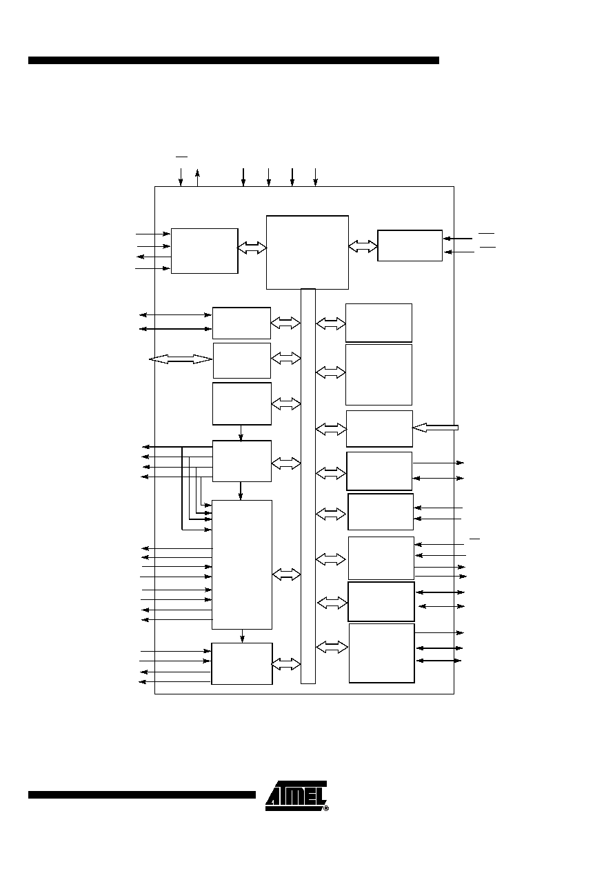
Description
The AT8xC51SND2C has been developed for handling MP3 ringing tones in mobile
phones and can replace sound generators while adding SD/MMC card reader, MP3
music decoding, and connection of the cell phone to a PC through USB. Cell phones
can also be used as a thumb drive extending cell phone capabilities.
The AT8xC51SND2C are fully integrated stand-alone hardwired MPEG I/II-Layer 3
decoder with a C51 microcontroller core handling data flow, MP3-player control, Stereo
Audio DAC and Mono Audio Power Amplifier for speaker control.
The AT89C51SND2C includes 64K Bytes of Flash memory and allows In-System Pro-
gramming through an embedded 4K Bytes of Boot Flash memory.
The AT83SND2C includes 64K Bytes of ROM memory.
The AT8xC51SND2C include 2304 Bytes of RAM memory.
The AT8xC51SND2C provides the necessary features for human interface like timers,
keyboard port, serial or parallel interface (USB, TWI, SPI, IDE), I
2
S output, and all exter-
nal memory interface (NAND or NOR Flash, SmartMedia, MultiMedia, DataFlash cards).
Typical Applications
�
MP3-Player
�
PDA, Camera, Mobile Phone MP3
�
Car Audio/Multimedia MP3
�
Home Audio/Multimedia MP3
5
AT8xC51SND2C
4341E�MP3�06/05
Signals
All the AT8xC51SND2C signals are detailed by functionality in Table 1 to Table 14.
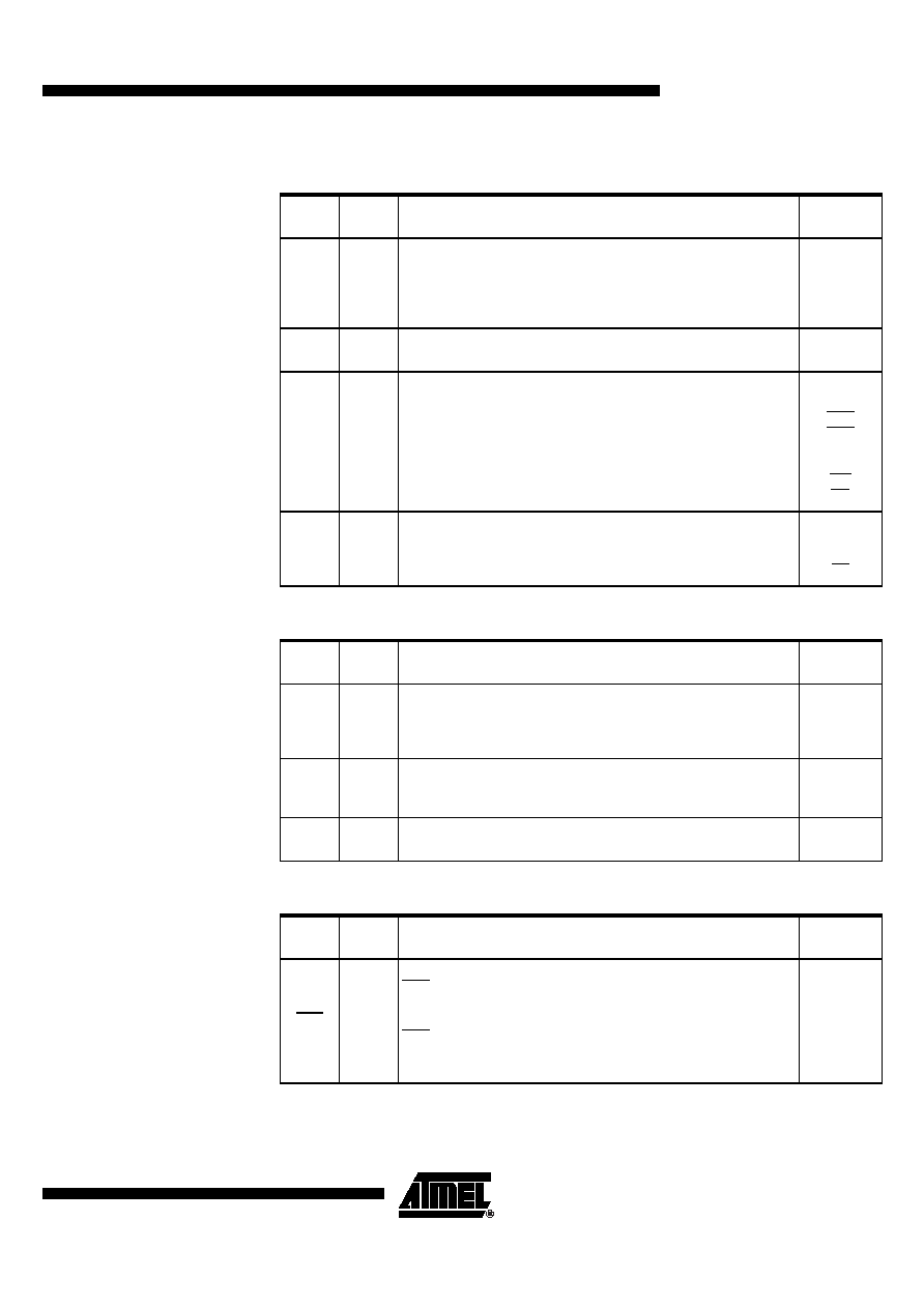
Table 1. Ports Signal Description
Table 2. Clock Signal Description
Table 3. Timer 0 and Timer 1 Signal Description
Signal
Name
Type
Description
Alternate
Function
P0.7:0
I/O
Port 0
P0 is an 8-bit open-drain bidirectional I/O port. Port 0 pins that have 1s
written to them float and can be used as high impedance inputs. To
avoid any parasitic current consumption, floating P0 inputs must be
polarized to V
DD
or V
SS
.
AD7:0
P2.7:0
I/O
Port 2
P2 is an 8-bit bidirectional I/O port with internal pull-ups.
A15:8
P3.7:0
I/O
Port 3
P3 is an 8-bit bidirectional I/O port with internal pull-ups.
RXD
TXD
INT0
INT1
T0
T1
WR
RD
P4.3:0
I/O
Port 4
P4 is an 8-bit bidirectional I/O port with internal pull-ups.
MISO
MOSI
SCK
SS
Signal
Name
Type
Description
Alternate
Function
X1
I
Input to the on-chip inverting oscillator amplifier
To use the internal oscillator, a crystal/resonator circuit is connected to
this pin. If an external oscillator is used, its output is connected to this
pin. X1 is the clock source for internal timing.
-
X2
O
Output of the on-chip inverting oscillator amplifier
To use the internal oscillator, a crystal/resonator circuit is connected to
this pin. If an external oscillator is used, leave X2 unconnected.
-
FILT
I
PLL Low Pass Filter input
FILT receives the RC network of the PLL low pass filter.
-
Signal
Name
Type
Description
Alternate
Function
INT0
I
Timer 0 Gate Input
INT0 serves as external run control for timer 0, when selected by
GATE0 bit in TCON register.
External Interrupt 0
INT0 input sets IE0 in the TCON register. If bit IT0 in this register is set,
bit IE0 is set by a falling edge on INT0#. If bit IT0 is cleared, bit IE0 is
set by a low level on INT0#.
P3.2