
1
4234ESCR09/04
Features
·
Smart Card Interface
Compliance with ISO 7816, EMV2000, GIE-CB, GSM and WHQL Standards
Card Clock Stop High or Low for Card Power-down Modes
Support Synchronous Cards with C4 and C8 Contacts
Card Detection and Automatic de-activation Sequence
Programmable Activation Sequence
Direct Connection to the Smart Card
Logic Level Shifters
Short Circuit Current Limitation (see electrical characteristics)
8kV+ ESD Protection (MIL/STD 883 Class 3)
Programmable Voltage
5V ±5% at 65 mA (Class A)
3V ±0.2V at 65 mA (Class B)
1.8V ±0.14V at 40 mA
Low Ripple Noise: < 200 mV
·
Versatile Host Interface
ICAM (Conditional Access) Compatible
Two Wire Interface (TWI) Link
Programmable Address Allow up to 8 Devices
Programmable Interrupt Output
Automatic Level Shifter (1.6V to V
CC
)
·
Reset Output Includes
Power-On Reset (POR)
Power-Fail Detector (PFD)
·
High-efficiency Step-up Converter: 80 to 98% Efficiency
·
Extended Voltage Operation: 3V to 5.5V
·
Low Power Consumption
180 mA Maximum In-rush Current
30
µ
A Typical Power-down Current (without Smart Card)
·
4 to 48 MHz Clock Input, 7 MHz Min for Step-up Converter (for AT83C24)
·
18 to 48MHz Clock input (for AT83C24NDS)
·
Industrial Temperature Range: -40 to +85
°
C
·
Packages: SO28 and QFN28
Description
The AT83C24 is a smart card reader interface IC for smart card reader/writer applica-
tions such as EFT/POS terminals and set top boxes. It enables the management of
any type of smart card from any kind of host. Up to 8 AT83C24 can be connected in
parallel using the programmable TWI address.
Its high efficiency DC/DC converter, low quiescent current in standby mode makes it
particularly suited to low power and portable applications. The reduced bill of material
allows reducing significantly the system cost. A sophisticated protection system guar-
antees timely and controlled shutdown upon error conditions.
The AT83C24NDS is a dedicated version approved by NDS for use with NDS Video-
Guard conditional access software in set-top boxes. All AT83C24 datasheet is
app licab le to AT83 C24N DS. T he m ain difference s b etween AT 83C2 4 and
AT83C24NDS are listed below:
1/
CLASS A card supplied with CVCC = 4.75 to 5.25V for AT83C24NDS,
CLASS A card supplied with CVCC = 4.6 to 5.25V for AT83C24
2/
18MHz minimum on input clock for AT83C24NDS
3/
Up to 10µF for capacitor connected on CVCC pin for AT83C24,
3.3µF mandatory for AT83C24NDS
Smart Card
Reader
Interface with
Power
Management
AT83C24
AT83C24NDS

2
AT83C24
4234ESCR09/04
Acronyms
TWI: Two-wire Interface
POR: Power On Reset
PFD: Power Fail Detect
ART: Automatic Reset Transition
ATR: Answer To Reset
MSB: Most Significant Bit
LSB: Least Significant bit
SCIB: Smart Card Interface Bus
Block Diagram
PRES/ INT
CLK
VSS
CRST
CPRES
CIO, CC4, CC8
CCLK
CVCC
LI
RESET
Voltage
supervisor
POR/PFD
TWI
Controller
Clocks Controller
DC/DC
Converter
Analog
Drivers
SCL
SDA
I/O, C4, C8
DVCC
EVCC
A2/CK, A1/RST, A0/3V, CMDVCC
Timer
16 Bits
Main
Control
& Logic Unit
CVSS
CVCCIN
VCC
3
AT83C24
4234ESCR09/04
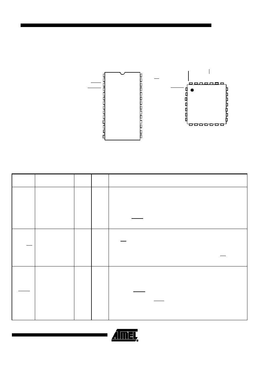
Pin Description
Pinouts (Top View)
28-pin SOIC Pinout
QFN28 pinout
Note:
1. NC = Not Connected
2. SOIC and QFN packages are available for
AT83C24 and for AT83C24NDS
Signals
A1
A2
A0
1
EVCC
CCLK
CRST
SCL
VCC
RESET
CVSS
CVCCin
I/O
CLK
2
3
4
5
6
7
8
9
10
28
27
26
25
24
23
22
21
20
19
LI
PRES/INT
DVCC
VSS
SDA
CPRES
12
18
17
11
C8
CIO
C4
16
15
CC8
CMDVCC
CC4
1
VSS
V
CC
CVSS
LI
2
3
4
5
6
7
8
9 10 11 12 13 14
16
15
17
18
19
20
21
22
23
24
25
26
27
28
TOP VIEW
QFN 28
CIO
CC
8
CVCCin
CRS
T
CP
RE
S
CC
4
CC
L
K
CMDVCC
R
ESET
DV
CC
C8
CL
K
PR
E
S
/
I
N
T
C4
/CK
/CK
/RST
A0
/RST
/3V
/3V
CVCC
CVCC
SDA
SCL
A1
A2
I/O
EVCC
13
14
NC
NC
NC
NC
Table 1. Ports Description
Pad Name
Pad Internal
Power Supply
ESD
Limits
Pad
Type
Description
A2/CK-
A1/RST-
A0/3V
EVCC
3 kV
I
Microcontroller Interface Function:
TWI bus slave address selection input.
A2/CK and A1/RST pins are respectively connected to CCLK and CRST signals in
"transparent mode" (see page 18 ).
A0/3V is used for hardware activation to select CVCC voltage (3V or 5V).
The slave address of the device is based on the value present on A2, A1, A0 on the
rising edge of RESET pin (see Table 2). In fact, the address is taken internally at the 11th
CLK rising edge.
PRES/INT
EVCC
3 kV
O
open-
drain
Microcontroller Interface Function:
Depending on IT_SEL value (see CONFIG4 register),
PRES/INT outputs card presence status or interruptions (page 9)
An internal Pull-up (typ 330k
,
see Table 18)to EVCC can be activated in the pad if
necessary using INT_PULLUP bit (CONFIG4 register).
Remark: during power up and before registers configuration, the PRES/INT signal must
be ignored.
RESET
VCC
3 kV
I/O
open-
drain
Microcontroller Interface Function:
·
Power-on reset
·
A low level on this pin keeps the AT83C24 under reset even if applied on power-on.
It also resets the AT83C24 if applied when the AT83C24 is running (see Power
monitoring §).
·
Asserting RESET when the chip is in Shut-down mode returns the chip to normal
operation.
·
AT83C24 is driving the Reset pin Low on power-on-reset or if power fail on V
CC
or
DVCC (see POWERMON bit in CONFIG4 register), this can be used to reset or
interrupt other devices. After reset, AT83C24 needs to be reconfigured before
starting a new card session.

4
AT83C24
4234ESCR09/04
SDA
VCC
3 kV
I/O
open-
drain
Microcontroller Interface Function
TWI serial data
SCL
VCC
3 kV
I/O
open-
drain
Microcontroller Interface Function
TWI serial clock
I/O
EVCC
3 kV
I/O
Microcontroller Interface Function
Copy of CIO pin and high level reference for EVCC.
An external pull up to EVCC is needed on IO pin.
I/O is the reference level for EVCC if EVCC is connected to a capacitor.
This feature is unused if EVCC is connected to VCC.
C4
EVCC
3 kV
I/O
(pull-up)
Microcontroller Interface Function
Copy of Card CC4.
C8
EVCC
3 kV
I/O
(pull-up)
Microcontroller Interface Function
Copy of Card CC8.
CLK
EVCC
3 kV
I
Microcontroller Interface Function
Master Clock
CIO
CVCC
8 kV+
I/O
(pull-up)
Smart card interface function
Card I/O
CC4
CVCC
8 kV+
I/O
(pull-up)
Smart card interface function
Card C4
CC8
CVCC
8 kV+
I/O
(pull-up)
Smart card interface function
Card C8
CPRES
VCC
8 kV+
I
(pull-up)
Smart card interface function
Card presence
An internal Pull-up to VCC can be activated in the pad if necessary using PULLUP bit
(CONFIG1 register).
CCLK
CVCC
8 kV+
O
Smart card interface function
Card clock
CRST
CVCC
8 kV+
O
Smart card interface function
Card reset
CMDVCC
EVCC
3 kV+
I
(pull-up)
Microcontroller Interface Function:
Activation/Shutdown of the smart card Interface.
VCC
3 kV+
PWR
Supply Voltage
V
CC
is used to power the internal voltage regulators and I/O buffers.
LI
3 kV+
PWR
DC/DC Input
LI must be tied to VCC pin through an external coil (typically 4.7
µ
H) and provides the
current for the charge pump of the DC/DC converter.
It may be directly connected to VCC if the step-up converter is not used (see STEPREG
bit in CONFIG4 register and see minimum VCC values in Table 20 (class A) and
Table 21 (class B)).
Table 1. Ports Description (Continued)
Pad Name
Pad Internal
Power Supply
ESD
Limits
Pad
Type
Description
5
AT83C24
4234ESCR09/04
Note:
ESD Test conditions: 3 positive and 3 negative pulses on each pin versus GND. Pulses
generated according to Mil/STD 883 Class3. Recommended capacitors soldered on
CVCC and VCC pins.
CVCC
8 kV+
PWR
Card Supply Voltage
CVCC is the programmable voltage output for the Card interface.
It must be connected to external decoupling capacitors (see page 35 and page 36).
CVCCin
8 kV+
PWR
Card Supply Voltage
This pin must be connected to CVCC.
DVCC
3 kV+
PWR
Digital Supply Voltage
Is internally generated and used to supply the digital core.
This pin has to be connected to an external capacitor of 100 nF and should not be
connected to other devices.
EVCC
3 kV+
PWR
Extra Supply Voltage (Microcontroller power supply)
EVCC is used to supply the internal level shifters of host interface pins.
EVCC voltage can be supplied from the external EVCC pin connected to the host power
supply.
If EVCC cannot be connected to the host power supply, it must be tied to an external
capacitor. EVCC voltage can be generated internally by an automatic follow up of the
logic high level on the I/O pin. In this configuration, connect a 100 nF + 100kOhms in
parallel between EVCC pin and VSS pin.
CVSS
8 kV+
GND
DC/DC Ground
CVSS is used to sink high shunt currents from the external coil.
VSS
GND
Ground
Table 1. Ports Description (Continued)
Pad Name
Pad Internal
Power Supply
ESD
Limits
Pad
Type
Description