1
Features
À
Single Voltage Read/Write Operation: 2.65V to 3.3V (BV), 3.0V to 3.6V (LV)
À
Access Time ¡ 85 ns
À
Sector Erase Architecture
¡ Sixty-three 32K Word (64K Bytes) Sectors with Individual Write Lockout
¡ Eight 4K Word (8K Bytes) Sectors with Individual Write Lockout
À
Fast Word Program Time ¡ 15 Ás
À
Fast Sector Erase Time ¡ 200 ms
À
Suspend/Resume Feature for Erase and Program
¡ Supports Reading and Programming from Any Sector by Suspending Erase
of a Different Sector
¡ Supports Reading Any Byte/Word by Suspending Programming of Any
Other Byte/Word
À
Low-power Operation
¡ 25 mA Active
¡ 10 ÁA Standby
À
Data Polling, Toggle Bit, Ready/Busy for End of Program Detection
À
VPP Pin for Write Protection
À
RESET Input for Device Initialization
À
Sector Lockdown Support
À
TSOP, CBGA and ÁBGA Package Options
À
Top or Bottom Boot Block Configuration Available
À
128-bit Protection Register
Description
The AT49BV/LV32X(T) is a 3.0-volt 32-megabit Flash m em or y organized as
2,097,152 words of 16 bits each or 4,194,304 bytes of 8 bits each. The x16 data
appears on I/O0 - I/O15; the x8 data appears on I/O0 - I/O7. The memory is divided
into 71 sectors for erase operations. The device is offered in 48-lead TSOP, and
48-ball CBGA and ÁBGA packages. The device has CE and OE control signals to
avoid any bus contention. This device can be read or reprogrammed using a single
power supply, making it ideally suited for in-system programming.
32-megabit
(2M x 16/4M x 8)
3-volt Only
Flash Memory
AT49BV320
AT49BV320T
AT49BV321
AT49BV321T
AT49LV320
AT49LV320T
AT49LV321
AT49LV321T
Recommend Using
AT49BV320A(T)/322A(T)
for New Designs.
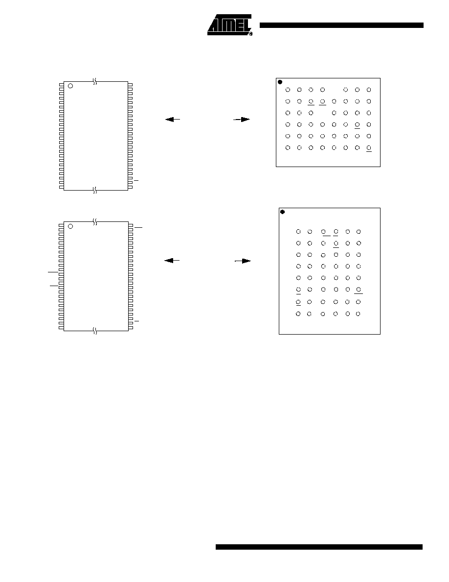
Pin Configurations
Pin Name
Function
A0 - A20
Addresses
CE
Chip Enable
OE
Output Enable
WE
Write Enable
RESET
Reset
RDY/BUSY
READY/BUSY Output
VPP
Write Protection
I/O0 - I/O14
Data Inputs/Outputs
I/O15 (A-1)
I/O15 (Data Input/Output, Word Mode)
A-1 (LSB Address Input, Byte Mode)
BYTE
Selects Byte or Word Mode
NC
No Connect
VCCQ
Output Power Supply
Rev. 1494H¡FLASH¡01/03
2
AT49BV/LV320(T)/321(T)
1494H¡FLASH¡01/03
TSOP Top View
Type 1
TSOP Top View
Type 1
1
2
3
4
5
6
7
8
9
10
11
12
13
14
15
16
17
18
19
20
21
22
23
24
48
47
46
45
44
43
42
41
40
39
38
37
36
35
34
33
32
31
30
29
28
27
26
25
A15
A14
A13
A12
A11
A10
A9
A8
NC
A20
WE
RESET
VPP
NC
A19
A18
A17
A7
A6
A5
A4
A3
A2
A1
A16
VCCQ
GND
I/O15
I/O7
I/O14
I/O6
I/O13
I/O5
I/O12
I/O4
VCC
I/O11
I/O3
I/O10
I/O2
I/O9
I/O1
I/O8
I/O0
OE
GND
CE
A0
1
2
3
4
5
6
7
8
9
10
11
12
13
14
15
16
17
18
19
20
21
22
23
24
48
47
46
45
44
43
42
41
40
39
38
37
36
35
34
33
32
31
30
29
28
27
26
25
A15
A14
A13
A12
A11
A10
A9
A8
A19
A20
WE
RESET
VPP
NC
RDY/BUSY
A18
A17
A7
A6
A5
A4
A3
A2
A1
A16
BYTE
GND
I/O15/A-1
I/O7
I/O14
I/O6
I/O13
I/O5
I/O12
I/O4
VCC
I/O11
I/O3
I/O10
I/O2
I/O9
I/O1
I/O8
I/O0
OE
GND
CE
A0
ÁBGA Top View (Ball Down)
CBGA Top View (Ball Down)
A
B
C
D
E
F
1
2
3
4
5
6
7
A13
A14
A15
A16
VCCQ
GND
A11
A10
A12
I/O14
I/O15
I/O7
A8
WE
A9
I/O5
I/O6
I/O13
VPP
RST
I/O11
I/O12
I/O4
A18
A20
I/O2
I/O3
VCC
A19
A17
A6
I/O8
I/O9
I/O10
A7
A5
A3
CE
I/O0
I/O1
A4
A2
A1
A0
GND
OE
8
A
B
C
D
E
F
G
H
1
2
3
4
5
6
RDY/BUSY
NC
A18
A20
I/O2
I/O10
I/O11
I/O3
A3
A4
A2
A1
A0
CE
OE
VSS
A7
A17
A6
A5
I/O0
I/O8
I/O9
I/O1
WE
RST
Vpp
A19
I/O5
I/O12
VCC
I/O4
A9
A8
A10
A11
I/O7
I/O14
I/O13
I/O6
A13
A12
A14
A15
A16
BTYE
I/015/A-1
VSS
AT49BV320(T)
AT49BV/LV320(T)
AT49BV/LV321(T)

3
AT49BV/LV320(T)/321(T)
1494H¡FLASH¡01/03
The device powers on in the read mode. Command sequences are used to place the device in
other operation modes such as program and erase. The device has the capability to protect
the data in any sector (see "Sector Lockdown" section).
To increase the flexibility of the device, it contains an Erase Suspend and Program Suspend
feature. This feature will put the erase or program on hold for any amount of time and let the
user read data from or program data to any of the remaining sectors within the memory. The
end of a program or an erase cycle is detected by the READY/BUSY pin, Data Polling or by
the toggle bit.
The VPP pin provides data protection. When the V
PP
input is below 0.8V, the program and
erase functions are inhibited. When V
PP
is at 1.65V or above, normal program and erase oper-
ations can be performed.
A six-byte command (Enter Single Pulse Program Mode) sequence to remove the requirement
of entering the three-byte program sequence is offered to further improve programming time.
After entering the six-byte code, only single pulses on the write control lines are required for
writing into the device. This mode (Single Pulse Byte/Word Program) is exited by powering
down the device, or by pulsing the RESET pin low for a minimum of 500 ns and then bringing
it back to V
CC
. Erase, Erase Suspend/Resume and Program Suspend/Resume commands will
not work while in this mode; if entered they will result in data being programmed into the
device. It is not recommended that the six-byte code reside in the software of the final product
but only exist in external programming code.
When using the AT49BV/LV320(T) pinout configuration, the device always operates in the
word mode. In the AT49BV/LV321(T) configuration, the BYTE pin controls whether the device
data I/O pins operate in the byte or word configuration. If the BYTE pin is set at logic "1", the
device is in word configuration, I/O0 - I/O15 are active and controlled by CE and OE.
If the BYTE pin is set at logic "0", the device is in byte configuration, and only data I/O pins
I/O0 - I/O7 are active and controlled by CE and OE. The data I/O pins I/O8 - I/O14 are tri-
stated, and the I/O15 pin is used as an input for the LSB (A-1) address function.
4
AT49BV/LV320(T)/321(T)
1494H¡FLASH¡01/03
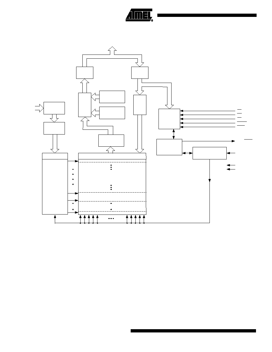
Block Diagram
IDENTIFIER
REGISTER
STATUS
REGISTER
DATA
COMPARATOR
OUTPUT
MULTIPLEXER
OUTPUT
BUFFER
INPUT
BUFFER
COMMAND
REGISTER
DATA
REGISTER
Y-GATING
WRITE STATE
MACHINE
PROGRAM/ERASE
VOLTAGE SWITCH
CE
WE
OE
RESET
BYTE
RDY/BUSY
VPP
VCC
GND
Y-DECODER
X-DECODER
INPUT
BUFFER
ADDRESS
LATCH
I/O0 - I/O15/A-1
A0 - A20
MAIN
MEMORY

5
AT49BV/LV320(T)/321(T)
1494H¡FLASH¡01/03
Device
Operation
READ: The AT49BV/LV32X(T) is accessed like an EPROM. When CE and OE are low and
WE is high, the data stored at the memory location determined by the address pins are
asserted on the outputs. The outputs are put in the high impedance state whenever CE or OE
is high. This dual-line control gives designers flexibility in preventing bus contention.
COMMAND SEQUENCES: When the device is first powered on, it will be reset to the read or
standby mode, depending upon the state of the control line inputs. In order to perform other
device functions, a series of command sequences are entered into the device. The command
sequences are shown in the "Command Definition in Hex" table on page 12 (I/O8 - I/O15 are
don't care inputs for the command codes). The command sequences are written by applying a
low pulse on the WE or CE input with CE or WE low (respectively) and OE high. The address
is latched on the falling edge of CE or WE, whichever occurs last. The data is latched by the
first rising edge of CE or WE. Standard microprocessor write timings are used. The address
locations used in the command sequences are not affected by entering the command
sequences.
RESET: A RESET input pin is provided to ease some system applications. When RESET is at
a logic high level, the device is in its standard operating mode. A low level on the RESET input
halts the present device operation and puts the outputs of the device in a high impedance
state. When a high level is reasserted on the RESET pin, the device returns to the read or
standby mode, depending upon the state of the control inputs.
ERASURE: Before a byte/word can be reprogrammed, it must be erased. The erased state of
memory bits is a logical "1". The entire device can be erased by using the Chip Erase com-
mand or individual sectors can be erased by using the Sector Erase command.
CHIP ERASE: The entire device can be erased at one time by using the six-byte chip erase
software code. After the chip erase has been initiated, the device will internally time the erase
operation so that no external clocks are required. The maximum time to erase the chip is t
EC
.
If the sector lockdown has been enabled, the chip erase will not erase the data in the sector
that has been locked out; it will erase only the unprotected sectors. After the chip erase, the
device will return to the read or standby mode.
SECTOR ERASE: As an alternative to a full chip erase, the device is organized into 71 sec-
tors (SA0 - SA70) that can be individually erased. The Sector Erase command is a six-bus
cycle operation. The sector address is latched on the falling WE edge of the sixth cycle while
the 30H data input command is latched on the rising edge of WE. The sector erase starts after
the rising edge of WE of the sixth cycle. The erase operation is internally controlled; it will
automatically time to completion. The maximum time to erase a sector is t
SEC
. When the sec-
tor programming lockdown feature is not enabled, the sector will erase (from the same Sector
Erase command). An attempt to erase a sector that has been protected will result in the oper-
ation terminating in 2 Ás.
BYTE/WORD PROGRAMMING: Once a memory block is erased, it is programmed (to a logi-
cal "0") on a byte-by-byte or on a word-by-word basis. Programming is accomplished via the
internal device command register and is a four-bus cycle operation. The device will automati-
cally generate the required internal program pulses.
Any commands written to the chip during the embedded programming cycle will be ignored. If
a hardware reset happens during programming, the data at the location being programmed
will be corrupted. Please note that a data "0" cannot be programmed back to a "1"; only erase
operations can convert "0"s to "1"s. Programming is completed after the specified t
BP
cycle
time. The Data Polling feature or the Toggle Bit feature may be used to indicate the end of a
program cycle. If the erase/program status bit is a "1", the device was not able to verify that the
erase or program operation was performed successfully.