1
Features
·
Single 2.7V - 3.6V Supply
·
Serial Peripheral Interface (SPI) Compatible
·
Page Program Operation
Single Cycle Reprogram (Erase and Program)
1024 Pages (264 Bytes/Page) Main Memory
·
Supports Page and Block Erase Operations
·
Two 264-byte SRAM Data Buffers Allows Receiving of Data
while Reprogramming of Nonvolatile Memory
·
Continuous Read Capability through Entire Array
Ideal for Code Shadowing Applications
·
Low Power Dissipation
4 mA Active Read Current Typical
2 µA CMOS Standby Current Typical
·
20 MHz Max Clock Frequency
·
Hardware Data Protection Feature
·
100% Compatible to AT45DB021 and AT45DB021A
·
5.0V-tolerant Inputs: SI, SCK, CS, RESET and WP Pins
·
Commercial and Industrial Temperature Ranges
Description
The AT45DB021B is a 2.7-volt only, serial interface Flash memory ideally suited for
a wide variety of digital voice-, image-, program code- and data-storage applications.
Its 2,162,688 bits of memory are organized as 1024 pages of 264 bytes each. In addi-
tion to the main memory, the AT45DB021B also contains two SRAM data buffers
of 264 bytes each. The buffers allow receiving of data while a page in the main mem-
ory is being reprogrammed, as well as reading or writing a continuous data stream.
2-megabit
2.7-volt Only
DataFlash
®
AT45DB021B
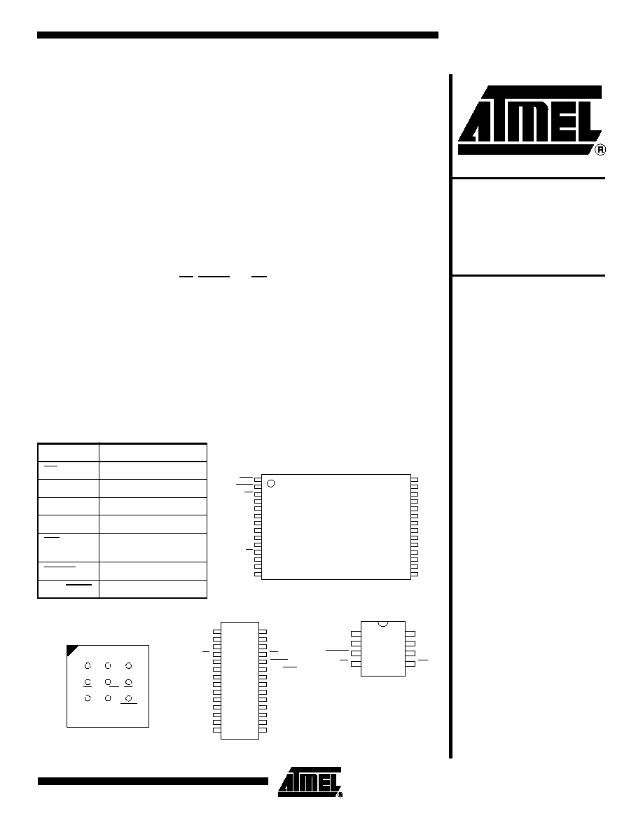
Pin Configurations
Pin Name
Function
CS
Chip Select
SCK
Serial Clock
SI
Serial Input
SO
Serial Output
WP
Hardware Page Write
Protect Pin
RESET
Chip Reset
RDY/BUSY
Ready/Busy
CBGA Top View
through Package
A
B
C
1
2
3
VCC
WP
RESET
GND
RDY/BSY
SI
SCK
CS
SO
TSOP Top View
Type 1
1
2
3
4
5
6
7
8
9
10
11
12
13
14
28
27
26
25
24
23
22
21
20
19
18
17
16
15
RDY/BUSY
RESET
WP
NC
NC
VCC
GND
NC
NC
NC
CS
SCK
SI
SO
NC
NC
NC
NC
NC
NC
NC
NC
NC
NC
NC
NC
NC
NC
28-SOIC
1
2
3
4
5
6
7
8
9
10
11
12
13
14
28
27
26
25
24
23
22
21
20
19
18
17
16
15
GND
NC
NC
CS
SCK
SI
SO
NC
NC
NC
NC
NC
NC
NC
VCC
NC
NC
WP
RESET
RDY/BUSY
NC
NC
NC
NC
NC
NC
NC
NC
8-SOIC
1
2
3
4
8
7
6
5
SI
SCK
RESET
CS
SO
GND
VCC
WP
Rev. 1937FDFLSH10/02
2
AT45DB021B
1937FDFLSH10/02
EEPROM emulation (bit or byte alterability) is easily handled with a self-contained three
step Read-Modify-Write operation. Unlike conventional Flash memories that are
accessed randomly with multiple address lines and a parallel interface, the DataFlash
uses a SPI serial interface to sequentially access its data. DataFlash supports SPI mode
0 and mode 3. The simple serial interface facilitates hardware layout, increases system
reliability, minimizes switching noise, and reduces package size and active pin count.
The device is optimized for use in many commercial and industrial applications where
high density, low pin count, low voltage, and low power are essential. The device oper-
ates at clock frequencies up to 20 MHz with a typical active read current consumption of
4 mA.
To allow for simple in-system reprogrammability, the AT45DB021B does not require
high input voltages for programming. The device operates from a single power supply,
2.7V to 3.6V, for both the program and read operations. The AT45DB021B is enabled
through the chip select pin (CS) and accessed via a three-wire interface consisting of
the Serial Input (SI), Serial Output (SO), and the Serial Clock (SCK).
All programming cycles are self-timed, and no separate erase cycle is required before
programming.
When the device is shipped from Atmel, the most significant page of the memory array
may not be erased. In other words, the contents of the last page may not be filled with
FFH.
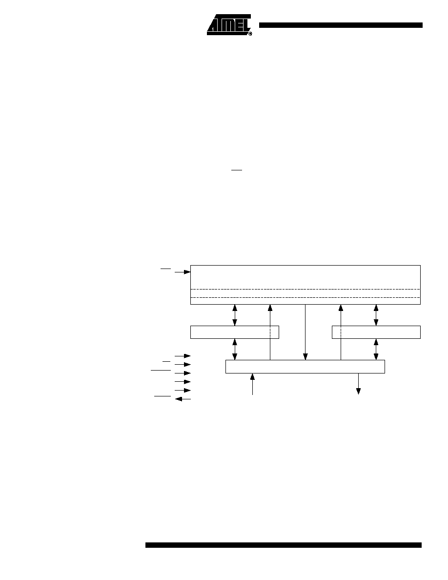
Block Diagram
Memory Array
To provide optimal flexibility, the memory array of the AT45DB021B is divided into three
levels of granularity comprised of sectors, blocks and pages. The Memory Architecture
Diagram illustrates the breakdown of each level and details the number of pages per
sector and block. All program operations to the DataFlash occur on a page-by-page
basis; however, the optional erase operations can be performed at the block or page
level.
FLASH MEMORY ARRAY
PAGE (264 BYTES)
BUFFER 2 (264 BYTES)
BUFFER 1 (264 BYTES)
I/O INTERFACE
SCK
CS
RESET
VCC
GND
RDY/BUSY
WP
SO
SI

3
AT45DB021B
1937FDFLSH10/02
Memory Architecture Diagram
Device Operation
The device operation is controlled by instructions from the host processor. The list of
instructions and their associated opcodes are contained in Tables 1 through 4 (pages 10
and 11). A valid instruction starts with the falling edge of CS followed by the appropriate
8-bit opcode and the desired buffer or main memory address location. While the CS pin
is low, toggling the SCK pin controls the loading of the opcode and the desired buffer or
main memory address location through the SI (serial input) pin. All instructions,
addresses, and data are transferred with the most significant bit (MSB) first.
Buffer addressing is referenced in the datasheet using the terminology BFA8 - BFA0 to
denote the nine address bits required to designate a byte address within a buffer. Main
memory addressing is referenced using the terminology PA9 -PA0 and BA8 -BA0 where
PA9 -PA0 denotes the 10 address bits required to designate a page address and BA8 -
BA0 denotes the nine address bits required to designate a byte address within the page.
Read Commands
By specifying the appropriate opcode, data can be read from the main memory or from
either one of the two data buffers. The DataFlash supports two categories of read
modes in relation to the SCK signal. The differences between the modes are in respect
to the inactive state of the SCK signal as well as which clock cycle data will begin to be
output. The two categories, which are comprised of four modes total, are defined as
Inactive Clock Polarity Low or Inactive Clock Polarity High and SPI Mode 0 or SPI
Mode 3. A separate opcode (refer to Table 1 on page 10 for a complete list) is used to
select which category will be used for reading. Please refer to the "Detailed Bit-level
Read Timing" diagrams in this datasheet for details on the clock cycle sequences for
each mode.
CONTINUOUS ARRAY READ: By supplying an initial starting address for the main
memory array, the Continuous Array Read command can be utilized to sequentially
read a continuous stream of data from the device by simply providing a clock signal; no
additional addressing information or control signals need to be provided. The DataFlash
incorporates an internal address counter that will automatically increment on every clock
SECTOR 0a = 8 Pages
2112 bytes (2K + 64)
SECTOR 0b = 248 Pages
65,472 bytes (62K + 1984)
Block = 2112 bytes
(2K + 64)
8 Pages
SECTOR 0
SECTOR 1
Page = 264 bytes
(256 + 8)
PAGE 0
PAGE 1
PAGE 6
PAGE 7
PAGE 8
PAGE 9
PAGE 1022
PAGE 1023
BLOCK 0
PAGE 14
PAGE 15
PAGE 16
PAGE 17
PAGE 18
PAGE 1021
BLOCK 1
SECTOR ARCHITECTURE
BLOCK ARCHITECTURE
PAGE ARCHITECTURE
BLOCK 0
BLOCK 1
BLOCK 30
BLOCK 31
BLOCK 32
BLOCK 33
BLOCK 126
BLOCK 127
BLOCK 62
BLOCK 63
BLOCK 64
BLOCK 65
SECTOR 2
BLOCK 2
SECTOR 0c = 256 Pages
67,584 bytes (64K + 2K)
SECTOR 1 = 512 Pages
135,168 bytes (128K + 4K)

4
AT45DB021B
1937FDFLSH10/02
cycle, allowing one continuous read operation without the need of additional address
sequences. To perform a continuous read, an opcode of 68H or E8H must be clocked
into the device followed by 24 address bits and 32 don't care bits. The first five bits of
the 24-bit address sequence are reserved for upward and downward compatibility to
larger and smaller density devices (see Notes under "Command Sequence for
Read/Write Operations" diagram). The next 10 address bits (PA9 - PA0) specify which
page of the main memory array to read, and the last nine bits (BA8 -BA0) of the 24-bit
address sequence specify the starting byte address within the page. The 32 don't care
bits that follow the 24 address bits are needed to initialize the read operation. Following
the 32 don't care bits, additional clock pulses on the SCK pin will result in serial data
being output on the SO (serial output) pin.
The CS pin must remain low during the loading of the opcode, the address bits, the don't
care bits, and the reading of data. When the end of a page in main memory is reached
during a Continuous Array Read, the device will continue reading at the beginning of the
next page with no delays incurred during the page boundary crossover (the crossover
from the end of one page to the beginning of the next page). When the last bit in the
main memory array has been read, the device will continue reading back at the begin-
ning of the first page of memory. As with crossing over page boundaries, no delays will
be incurred when wrapping around from the end of the array to the beginning of the
array.
A low-to-high transition on the CS pin will terminate the read operation and tri-state the
SO pin. The maximum SCK frequency allowable for the Continuous Array Read is
defined by the f
CAR
specification. The Continuous Array Read bypasses both data buff-
ers and leaves the contents of the buffers unchanged.
MAIN MEMORY PAGE READ: A Main Memory Page Read allows the user to read data
directly from any one of the 1024 pages in the main memory, bypassing both of the data
buffers and leaving the contents of the buffers unchanged. To start a page read, an
opcode of 52H or D2H must be clocked into the device followed by 24 address bits and
32 don't care bits. The first five bits of the 24-bit address sequence are reserved bits, the
next 10 address bits (PA9 -PA0) specify the page address, and the next nine address
bits (BA8-BA0) specify the starting byte address within the page. The 32 don't care bits
which follow the 24 address bits are sent to initialize the read operation. Following the
32 don't care bits, additional pulses on SCK result in serial data being output on the SO
(serial output) pin. The CS pin must remain low during the loading of the opcode, the
address bits, the don't care bits and the reading of data. When the end of a page in main
memory is reached during a Main Memory Page Read, the device will continue reading
at the beginning of the same page. A low-to-high transition on the CS pin will terminate
the read operation and tri-state the SO pin.
BUFFER READ: Data can be read from either one of the two buffers, using different
opcodes to specify which buffer to read from. An opcode of 54H or D4H is used to read
data from buffer 1, and an opcode of 56H or D6H is used to read data from buffer 2. To
perform a Buffer Read, the eight bits of the opcode must be followed by 15 don't care
bits, nine address bits, and eight don't care bits. Since the buffer size is 264-bytes, nine
address bits (BFA8 -BFA0) are required to specify the first byte of data to be read from
the buffer. The CS pin must remain low during the loading of the opcode, the address
bits, the don't care bits and the reading of data. When the end of a buffer is reached, the
device will continue reading back at the beginning of the buffer. A low-to-high transition
on the CS pin will terminate the read operation and tri-state the SO pin.

5
AT45DB021B
1937FDFLSH10/02
STATUS REGISTER READ: The status register can be used to determine the device's
ready/busy status, the result of a Main Memory Page to Buffer Compare operation, or
the device density. To read the status register, an opcode of 57H or D7H must be
loaded into the device. After the last bit of the opcode is shifted in, the eight bits of the
status register, starting with the MSB (bit 7), will be shifted out on the SO pin during the
next eight clock cycles. The five most-significant bits of the status register will contain
device information, while the remaining three least-significant bits are reserved for future
use and will have undefined values. After bit 0 of the status register has been shifted
out, the sequence will repeat itself (as long as CS remains low and SCK is being tog-
gled) starting again with bit 7. The data in the status register is constantly updated, so
each repeating sequence will output new data.
Ready/Busy status is indicated using bit 7 of the status register. If bit 7 is a 1, then the
device is not busy and is ready to accept the next command. If bit 7 is a 0, then the
device is in a busy state. The user can continuously poll bit 7 of the status register by
stopping SCK at a low level once bit 7 has been output. The status of bit 7 will continue
to be output on the SO pin, and once the device is no longer busy, the state of SO will
change from 0 to 1. There are eight operations that can cause the device to be in a busy
state: Main Memory Page to Buffer Transfer, Main Memory Page to Buffer Compare,
Buffer to Main Memory Page Program with Built-in Erase, Buffer to Main Memory Page
Program without Built-in Erase, Page Erase, Block Erase, Main Memory Page Program,
and Auto Page Rewrite.
The result of the most recent Main Memory Page to Buffer Compare operation is indi-
cated using bit 6 of the status register. If bit 6 is a 0, then the data in the main memory
page matches the data in the buffer. If bit 6 is a 1, then at least one bit of the data in the
main memory page does not match the data in the buffer.
The device density is indicated using bits 5, 4, 3 and 2 of the status register. For the
AT45DB021B, the four bits are 0, 1, 0 and 1. The decimal value of these four binary bits
does not equate to the device density; the four bits represent a combinational code
relating to differing densities of Serial DataFlash devices, allowing a total of sixteen dif-
ferent density configurations.
Program and Erase
Commands
BUFFER WRITE: Data can be shifted in from the SI pin into either buffer 1 or buffer 2.
To load data into either buffer, an 8-bit opcode, 84H for buffer 1 or 87H for buffer 2, must
be followed by 15 don't care bits and nine address bits (BFA8 -BFA0). The nine address
bits specify the first byte in the buffer to be written. The data is entered following the
address bits. If the end of the data buffer is reached, the device will wrap around back to
the beginning of the buffer. Data will continue to be loaded into the buffer until a low-to-
high transition is detected on the CS pin.
BUFFER TO MAIN MEMORY PAGE PROGRAM WITH BUILT-IN ERASE: Data written
into either buffer 1 or buffer 2 can be programmed into the main memory. To start the
operation, an 8-bit opcode (83H for buffer 1 or 86H for buffer 2) must be followed by the
five reserved bits, 10 address bits (PA9 -PA0) that specify the page in the main memory
to be written, and nine additional don't care bits. When a low-to-high transition occurs on
the CS pin, the part will first erase the selected page in main memory to all 1s and then
program the data stored in the buffer into the specified page in the main memory. Both
the erase and the programming of the page are internally self-timed and should take
Status Register Format
Bit 7
Bit 6
Bit 5
Bit 4
Bit 3
Bit 2
Bit 1
Bit 0
RDY/BUSY
COMP
0
1
0
1
X
X