
Symbol
V
DS
V
GS
I
DM
T
J
, T
STG
Symbol
Typ
Max
31
40
59
75
R
JL
16
24
Maximum Junction-to-Lead
C
Steady-State
°C/W
Thermal Characteristics
Parameter
Units
Maximum Junction-to-Ambient
A
t 10s
R
JA
°C/W
°C/W
Absolute Maximum Ratings T
A
=25°C unless otherwise noted
V
V
±20
Pulsed Drain Current
B
Power Dissipation
T
A
=25°C
Gate-Source Voltage
Drain-Source Voltage
Maximum Junction-to-Ambient
A
Steady-State
11
9.3
50
Continuous Drain
Current
A
Maximum
Units
Parameter
T
A
=25°C
T
A
=70°C
30
W
Junction and Storage Temperature Range
A
P
D
°C
3
2.1
-55 to 150
T
A
=70°C
I
D
AO4422
N-Channel Enhancement Mode Field Effect Transistor
Jan 2003
Features
V
DS
(V) = 30V
I
D
= 11A
R
DS(ON)
< 15m
(V
GS
= 10V)
R
DS(ON)
< 24m
(V
GS
= 4.5V)
General Description
The AO4422 uses advanced trench technology to
provide excellent R
DS(ON)
and low gate charge. This
device is suitable for use as a load switch or in PWM
applications. The source leads are separated to allow
a Kelvin connection to the source, which may be
used to bypass the source inductance.
SOIC-8
G
S
S
S
D
D
D
D
G
D
S
Alpha & Omega Semiconductor, Ltd.

AO4422
Symbol
Min
Typ
Max
Units
BV
DSS
30
V
1
T
J
=55°C
5
I
GSS
100
nA
V
GS(th)
1
1.8
3
V
I
D(ON)
40
A
12.6
15
T
J
=125°C
16.8
21
19.6
24
m
g
FS
25
S
V
SD
0.75
1
V
I
S
4.3
A
C
iss
1040
pF
C
oss
180
pF
C
rss
110
pF
R
g
0.7
Q
g
(10V)
19.8
nC
Q
g
(4.5V)
9.8
nC
Q
gs
2.5
nC
Q
gd
3.5
nC
t
D(on)
4.5
ns
t
r
3.9
ns
t
D(off)
17.4
ns
t
f
3.2
ns
t
rr
17.5
ns
Q
rr
7.6
nC
Body Diode Reverse Recovery Time
Body Diode Reverse Recovery Charge I
F
=11A, dI/dt=100A/
µs
Drain-Source Breakdown Voltage
On state drain current
I
D
=250
µA, V
GS
=0V
V
GS
=4.5V, V
DS
=5V
V
GS
=10V, I
D
=11A
Reverse Transfer Capacitance
I
F
=11A, dI/dt=100A/
µs
Electrical Characteristics (T
J
=25°C unless otherwise noted)
STATIC PARAMETERS
Parameter
Conditions
I
DSS
µA
Gate Threshold Voltage
V
DS
=V
GS
I
D
=250
µA
V
DS
=24V, V
GS
=0V
V
DS
=0V, V
GS
= ±20V
Zero Gate Voltage Drain Current
Gate-Body leakage current
R
DS(ON)
Static Drain-Source On-Resistance
Forward Transconductance
Diode Forward Voltage
m
V
GS
=4.5V, I
D
=10A
I
S
=1A,V
GS
=0V
V
DS
=5V, I
D
=11A
Total Gate Charge
Gate Source Charge
Gate resistance
V
GS
=0V, V
DS
=0V, f=1MHz
Turn-On Rise Time
Turn-Off DelayTime
V
GS
=10V, V
DS
=15V, R
L
=1.35
,
R
GEN
=3
Turn-Off Fall Time
Maximum Body-Diode Continuous Current
Input Capacitance
Output Capacitance
Turn-On DelayTime
DYNAMIC PARAMETERS
V
GS
=10V, V
DS
=15V, I
D
=11A
Total Gate Charge
Gate Drain Charge
V
GS
=0V, V
DS
=15V, f=1MHz
SWITCHING PARAMETERS
A: The value of R
JA
is measured with the device mounted on 1in
2
FR-4 board with 2oz. Copper, in a still air environment with T
A
=25°C. The value
in any a given application depends on the user's specific board design. The current rating is based on the t
10s thermal resistance rating.
B: Repetitive rating, pulse width limited by junction temperature.
C. The R
JA
is the sum of the thermal impedence from junction to lead R
JL
and lead to ambient.
D. The static characteristics in Figures 1 to 6 are obtained using 80
µs pulses, duty cycle 0.5% max.
E. These tests are performed with the device mounted on 1 in
2
FR-4 board with 2oz. Copper, in a still air environment with T
A
=25°C. The SOA
curve provides a single pulse rating.
Alpha & Omega Semiconductor, Ltd.
AO4422
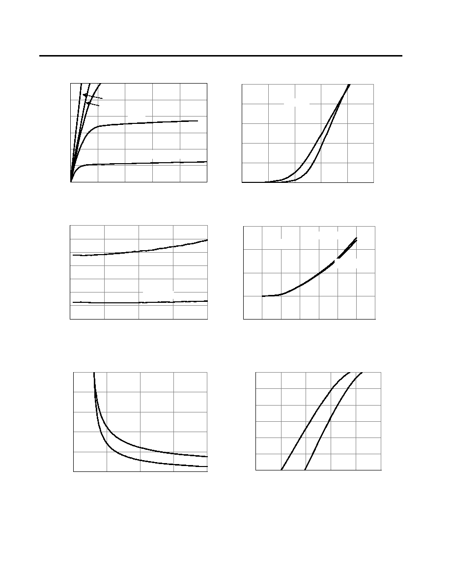
TYPICAL ELECTRICAL AND THERMAL CHARACTERISTICS
0
5
10
15
20
25
30
0
1
2
3
4
5
V
DS
(Volts)
Fig 1: On-Region Characteristics
I
D
(A
)
V
GS
=3V
3.5V
4V
4.5V
10V
0
4
8
12
16
20
1.5
2
2.5
3
3.5
4
V
GS
(Volts)
Figure 2: Transfer Characteristics
I
D
(A
)
10
12
14
16
18
20
22
24
0
5
10
15
20
I
D
(A)
Figure 3: On-Resistance vs. Drain Current and
Gate Voltage
R
DS
(
O
N)
(m
)
1.0E-05
1.0E-04
1.0E-03
1.0E-02
1.0E-01
1.0E+00
1.0E+01
0.0
0.2
0.4
0.6
0.8
1.0
V
SD
(Volts)
Figure 6: Body-Diode Characteristics
I
S
(A
)
25°C
125°C
0.8
1
1.2
1.4
1.6
0
25
50
75
100
125
150
175
Temperature (°C)
Figure 4: On-Resistance vs. Junction
Temperature
N
o
r
m
a
lized
On
-
R
esist
a
n
c
e
V
GS
=10V
V
GS
=4.5V
10
20
30
40
50
60
2
4
6
8
10
V
GS
(Volts)
Figure 5: On-Resistance vs. Gate-Source Voltage
R
DS
(
O
N)
(m
)
25°C
125°C
V
DS
=5V
V
GS
=4.5V
V
GS
=10V
I
D
=10A
25°C
125°C
I
D
=10A
Alpha & Omega Semiconductor, Ltd.
AO4422
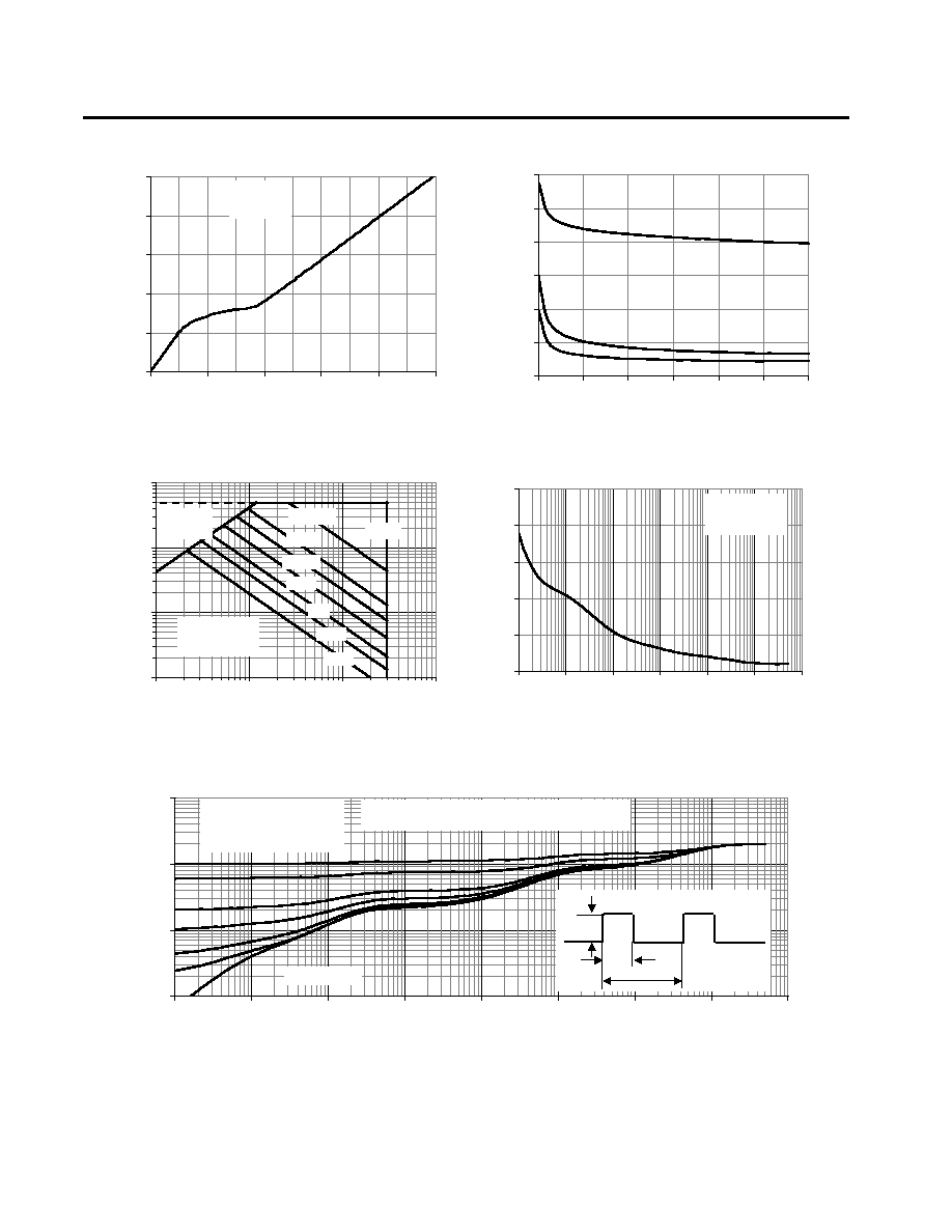
TYPICAL ELECTRICAL AND THERMAL CHARACTERISTICS
0
2
4
6
8
10
0
4
8
12
16
20
Q
g
(nC)
Figure 7: Gate-Charge Characteristics
V
GS
(V
ol
ts)
0
250
500
750
1000
1250
1500
0
5
10
15
20
25
30
V
DS
(Volts)
Figure 8: Capacitance Characteristics
C
a
p
acitan
ce (p
F
)
C
iss
0
10
20
30
40
50
0.001
0.01
0.1
1
10
100
1000
Pulse Width (s)
Figure 10: Single Pulse Power Rating Junction-to-
Ambient (Note E)
Po
w
e
r (
W
)
0.01
0.1
1
10
0.00001
0.0001
0.001
0.01
0.1
1
10
100
1000
Pulse Width (s)
Figure 11: Normalized Maximum Transient Thermal Impedance
Z
JA
N
o
r
m
a
liz
ed
T
r
an
sien
t
T
h
er
m
al R
esistan
ce
C
oss
C
rss
0.1
1.0
10.0
100.0
0.1
1
10
100
V
DS
(Volts)
I
D
(A
m
p
s)
Figure 9: Maximum Forward Biased Safe
Operating Area (Note E)
100
µs
10ms
1ms
0.1s
1s
10s
DC
R
DS(ON)
limited
T
J(Max)
=150°C
T
A
=25°C
V
DS
=15V
I
D
=11A
Single Pulse
D=T
on
/T
T
J,PK
=T
A
+P
DM
.Z
JA
.R
JA
R
JA
=40°C/W
T
on
T
P
D
In descending order
D=0.5, 0.3, 0.1, 0.05, 0.02, 0.01, single pulse
T
J(Max)
=150°C
T
A
=25°C
10
µs
Alpha & Omega Semiconductor, Ltd.