
P-Channel Enhancement Mode MOSFET
Copyright
ANPEC Electronics Corp.
Rev. A.1 - Sep., 2003
APM4429
www.anpec.com.tw
1
ANPEC reserves the right to make changes to improve reliability or manufacturability without notice, and advise
customers to obtain the latest version of relevant information to verify before placing orders.
Pin Description
Ordering and Marking Information
Features
Applications
·
Power Management in Notebook Computer,
Portable Equipment and Battery Powered
Systems
SO
-
8
·
-30V/-13A, R
DS(ON)
= 8m
(typ.) @ V
GS
= -20V
R
DS(ON)
= 9m
(typ.) @ V
GS
= -10V
R
DS(ON)
=13m
(typ.) @ V
GS
= -4.5V
··
··
·
Super High Density Cell Design
··
··
·
Reliable and Rugged
··
··
·
SO-8 Package
Symbol
Parameter
Rating
Unit
V
DSS
Drain-Source Voltage
-30
V
GSS
Gate-Source Voltage
±20
V
I
D
*
Maximum Drain Current Continuous T
A
= 25
°
C
-13
I
DM
Maximum Drain Current Pulsed
-50
A
* Surface Mounted on FR4 Board, t
10 sec.
Absolute Maximum Ratings
(T
A
= 25
°
C unless otherwise noted)
!
"
#
$
%
&
5
5
5
/
,
,
,
,
P-Channel MOSFET
G
D
S
S
S
D D D
A PM 4429
H a n d lin g C o d e
T e m p . R a ng e
P a c kag e C o d e
P a c ka g e C o d e
K : S O -8
O pe ra tio n J u n c tio n T e m p . R an g e
C : -5 5 to 1 5 0°C
H a n d lin g C o d e
T U : T u b e T R : T a p e & R e e l
L e a d F re e C o d e
L : L e a d F re e D e vic e B la n d : O rg ina l D e vice
A P M 4 4 2 9 K :
A P M 4 4 2 9
XXXX X
XXXX X - D a te C o d e
L e a d F re e C o d e
Copyright
ANPEC Electronics Corp.
Rev. A.1 - Sep., 2003
APM4429
www.anpec.com.tw
2
Symbol
Parameter
Rating
Unit
T
A
= 25
°
C
2.5
P
D
Maximum Power Dissipation
T
A
= 100
°
C
1.0
W
T
J
)
T
STG
Maximum Operating and Storage Junction Temperature
-55 to 150
°
C
R
JA
*
Thermal Resistance - Junction to Ambient
62.5
°C/W
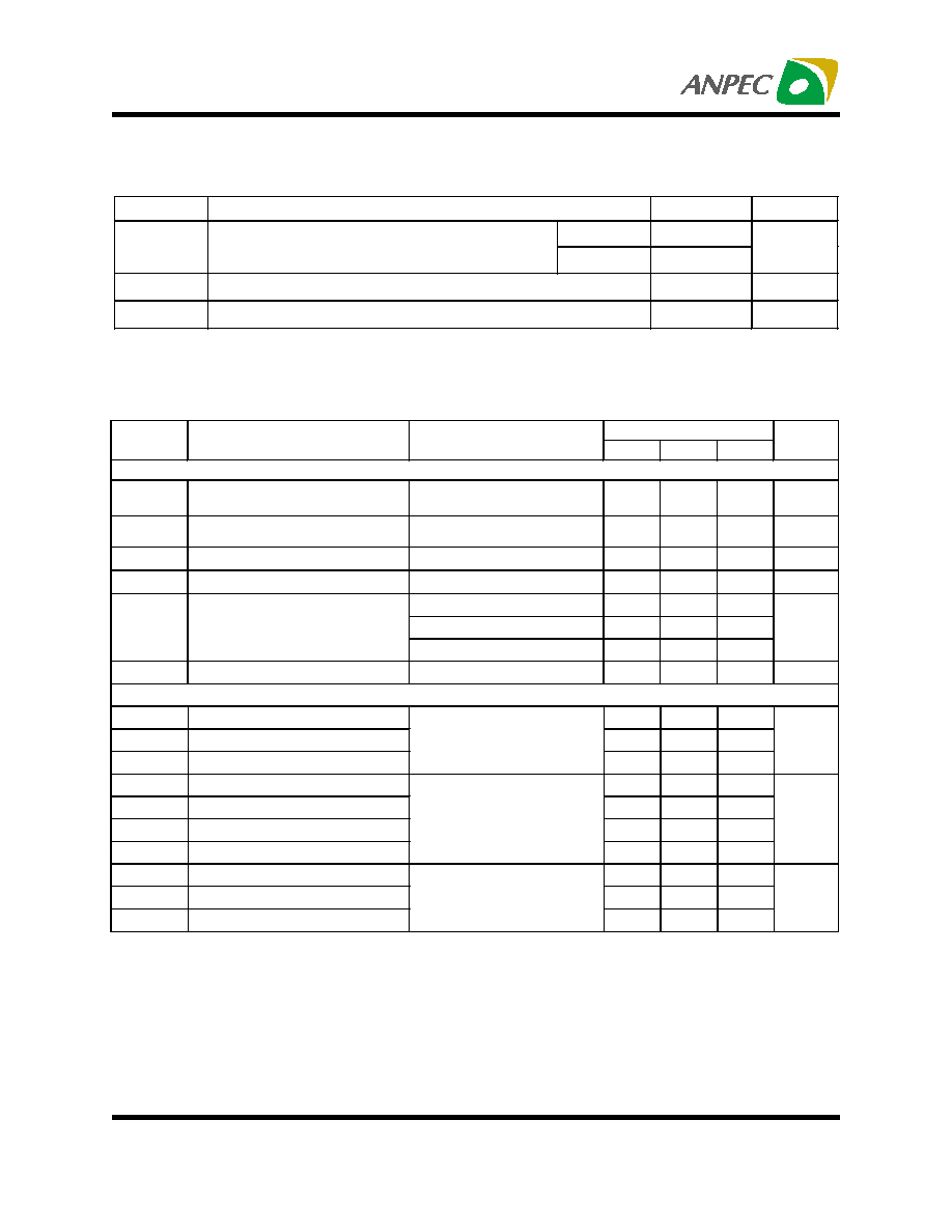
Electrical Characteristics
(T
A
= 25
°
C unless otherwise noted)
Absolute Maximum Ratings
(T
A
= 25
°
C unless otherwise noted)
APM 4429
Sym bol
Param eter
Test Condition
M in.
Typ
=
.
M ax.
Unit
Static
BV
D SS
D rain-Source Breakdown
Voltage
V
G S
=0V , I
D S
=-250
µ
A
-30
V
I
D SS
Zero G ate Voltage D rain
C urrent
V
D S
=-24V , V
G S
=0V
-1
µ
A
V
G S(th)
G ate T hreshold Voltage
V
D S
=V
G S
, I
D S
=-250
µ
A
-1
-1.5
-2
V
I
G SS
G ate Leakage C urrent
V
G S
=
±
20V , V
D S
=0V
±
100
nA
V
G S
=-20V , I
D S
=-13A
8
11
V
G S
=-10V , I
D S
=-13A
9
12
R
D S(O N )
D rain-Source O n-state
R esistance
>
V
G S
=-4.5V , I
D
=-12A
13
17
m
V
SD
D iode Forward Voltage
>
I
SD
=-3A, V
G S
=0V
-0.7
-1.3
V
Dynam ic
=
Q
g
Total G ate C harge
105
135
Q
gs
G ate-Source C harge
10.8
Q
gd
G ate-D rain C harge
V
D S
=-15V , V
G S
=-10V
l
D
=-13A
13.6
nC
t
d(O N )
Turn-on D elay Tim e
15
30
T
r
Turn-on R ise Tim e
20
30
t
d(O FF)
Turn-off D elay Tim e
55
85
T
f
Turn-off Fall Tim e
V
D D
=-15V , I
D
=-1A ,
V
G EN
=-10V , R
G
=6
R
L
=15
40
65
ns
C
iss
Input C apacitance
4730
C
oss
O utput C apacitance
800
C
rss
R everse Transfer C apacitance
V
G S
=0V
V
D S
=-25V
Frequency=1.0M H z
240
pF
Notes
a
: Pulse test ; pulse width
300
µ
s, duty cycle
2
%
b
: Guaranteed by design, not subject to production testing
Copyright
ANPEC Electronics Corp.
Rev. A.1 - Sep., 2003
APM4429
www.anpec.com.tw
3
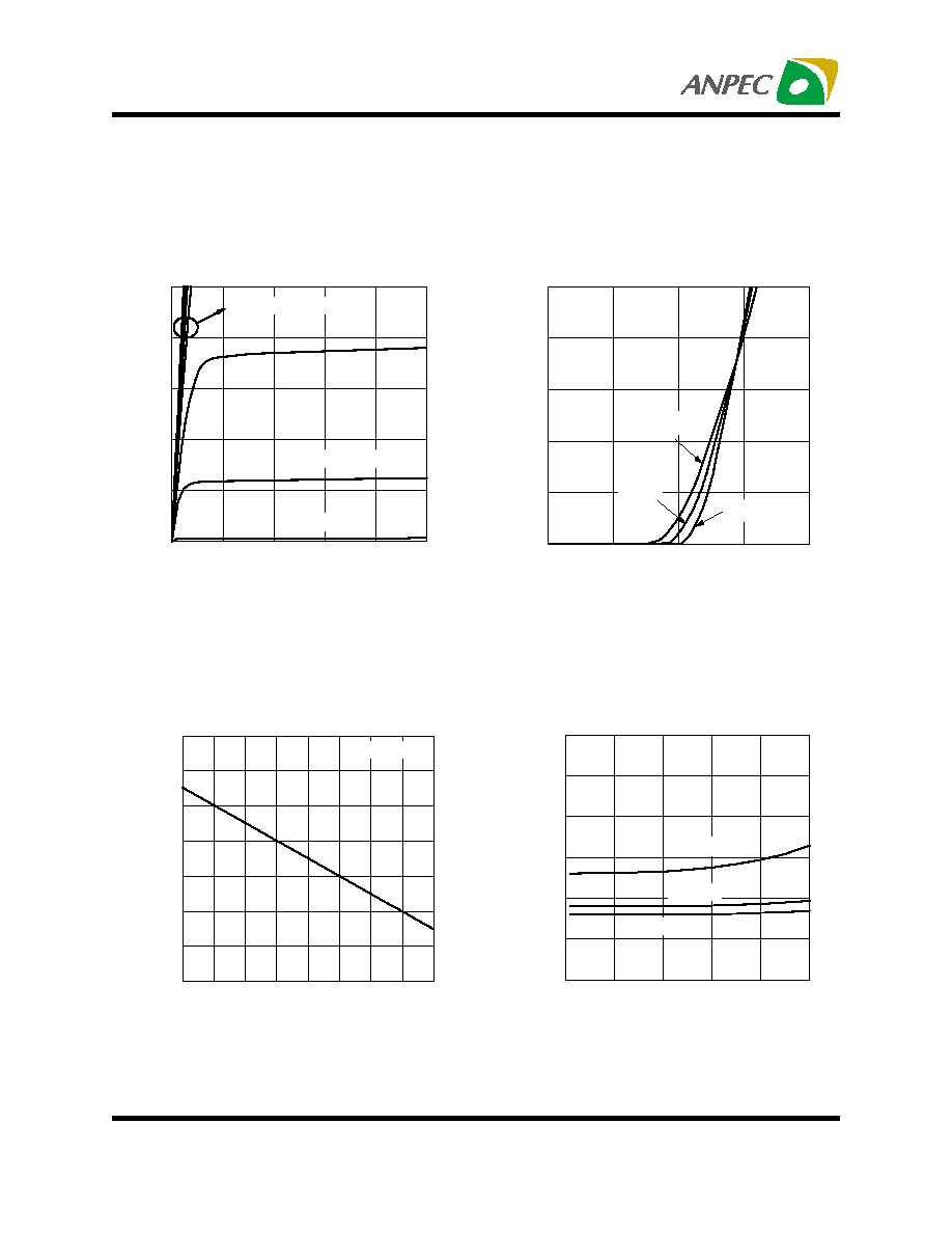
Typical Characteristics
-I
D-
Drain
Current
(
A)
Transfer Characteristics
-V
GS
- Gate-to-Source Voltage (V)
Threshold Voltage vs. Junction Temperature
Tj - Junction Temperature (°C)
-V
GS(th)-
Threshold
V
o
ltage
(V)
(Normalized)
On-Resistance vs. Drain Current
-I
D
- Drain Current (A)
R
DS(on)
-On-Resistance
(
)
Output Characteristics
-I
D
-Drain
Current
(A)
-V
DS
- Drain-to-Source Voltage (V)
0
1
2
3
4
0
10
20
30
40
50
T
j
=125
o
C
T
j
=25
o
C
T
j
=-55
o
C
-50 -25
0
25
50
75 100 125 150
0.00
0.25
0.50
0.75
1.00
1.25
1.50
1.75
-I
DS
=250
µ
A
0
20
40
60
80
100
0.000
0.005
0.010
0.015
0.020
0.025
0.030
-V
GS
=20V
-V
GS
=10V
-V
GS
=4.5V
0
2
4
6
8
10
0
10
20
30
40
50
-V
GS
=2.5V
-V
GS
=2V
-V
GS
=3V
-V
GS
= 4,5,6,7,8,9,10V
Copyright
ANPEC Electronics Corp.
Rev. A.1 - Sep., 2003
APM4429
www.anpec.com.tw
4
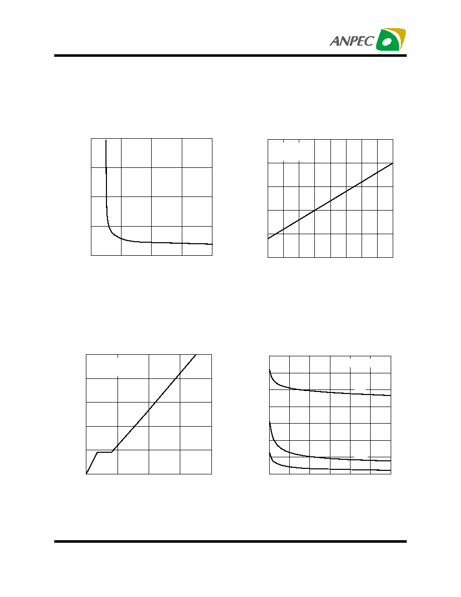
Typical Characteristics
-V
GS
- Gate-to-Source Voltage (V)
R
DS(on)
-On-Resistance
(
)
On-Resistance vs. Gate-to-Source Voltage
R
DS(on)
-On-Resistance
(
)
(Normalized)
On-Resistance vs. Junction Temperature
T
J
- Junction Temperature (°C)
-V
DS
- Drain-to-Source Voltage (V)
Capacitance
Capacitance
(pF)
Gate Charge
Q
G
- Gate Charge (nC)
-V
GS
-Gate-Source
V
o
ltage
(V)
0
5
10
15
20
0.00
0.02
0.04
0.06
0.08
-I
D
= 13A
-50 -25
0
25
50
75 100 125 150
0.50
0.75
1.00
1.25
1.50
1.75
-V
GS
= 10V
-I
D
= 13A
0
30
60
90
120
0
2
4
6
8
10
-V
DS
= 15 V
-I
D
= 13 A
0
5
10
15
20
25
30
0
1000
2000
3000
4000
5000
6000
7000
Frequency=1MHz
Crss
Coss
Ciss
Copyright
ANPEC Electronics Corp.
Rev. A.1 - Sep., 2003
APM4429
www.anpec.com.tw
5
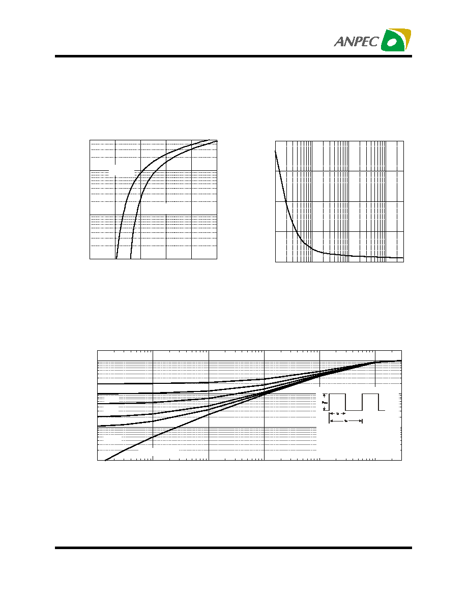
1E-4
1E-3
0.01
0.1
1
10
30
1E-3
0.01
0.1
1
2
D=0.02
D=0.05
D=0.1
D=0.2
Duty Cycle=0.5
SINGLE PULSE
1.Duty Cycle, D= t1/t2
2.Per Unit Base=R
thJA
=62.5
o
C/W
3.T
JM
-T
A
=P
DM
Z
thJA
4.Surface Mounted
0.0
0.4
0.8
1.2
1.6
2.0
0.1
1
10
50
T
j
=150
o
C
T
j
=25
o
C
Typical Characteristics
Single Pulse Power
Time (sec)
Square Wave Pulse Duration (sec)
Normalized
Effective
Transient
Thermal
I
mpedance
Normalized Thermal Transient Impedence, Junction to Ambient
Power
(
W)
Source-Drain Diode Forward Voltage
-V
SD
-Source-to-Drain Voltage (V )
-I
S
-Source
Current
(A)
0.01
0.1
1
10
30
0
30
60
90
120