Available on Tape
and Reel For Pick and
Place Manufacturing.
USA/Canada:
Toll Free:
Europe
:
(315) 432-8909
(800) 544-2414
+44 2392-232392
Model XDL20-3-050
Rev. B
Delay Line
Description
The XDL20-3-050 is a surface mount delay line that uses a slow wave
coupling structure that maximizes the amount of delay per unit area over
other distributed delay structures. The XDL20-3-050 can be used in
amplifier linearization applications from 850 2200 MHz. The XDL20-3-
050 is ideal for the delay element required in the main loop of feed forward
amplifiers. The Xinger® delay lines are a low cost, high quality alternative
to the traditional coaxial and filter solutions presently available. Parts have
been subjected to rigorous qualification testing and units are 100% tested
ELECTRICAL
SPECIFICATIONS
Frequency (MHz.)
869-894
AMPS Band
925-960
GSM Band
1805-1880
DCS Band
19301990
PCS Band
2110-2170
UMTS Band
Mean Delay (nS)
3.0
±
0.06
3.06
±
0.06
4.90
±
0.1
5.00
±
0.1
4.85
±
0.1
Deviation from Linear
Phase (Degrees Max)
±
0.50
±
0.50
±
1.00
±
1.00
±
1.00
Amplitude Flatness
(dB p-p)
0.10
0.10
0.15
0.10
0.10
Return Loss (dB min)
20
20
20
20
20
Insertion Loss (dB/nS)
0.40
0.45
0.55
0.55
0.60
Power Handling
(Watts)
40
40
40
40
40
Features:
·
Production Friendly
·
Consistent Delay
·
Stable over
Temperature
·
Surface Mountable
·
Available in
Tape&Reel
·
Non-Lead Solder
Paste Compatible
·
100% Tested
JC (°C/watts)
2
2
2
2
2
Specification based on performance of unit properly installed on microstrip printed circuit boards with 50
nominal impedance. Specifications subject to change without notice.
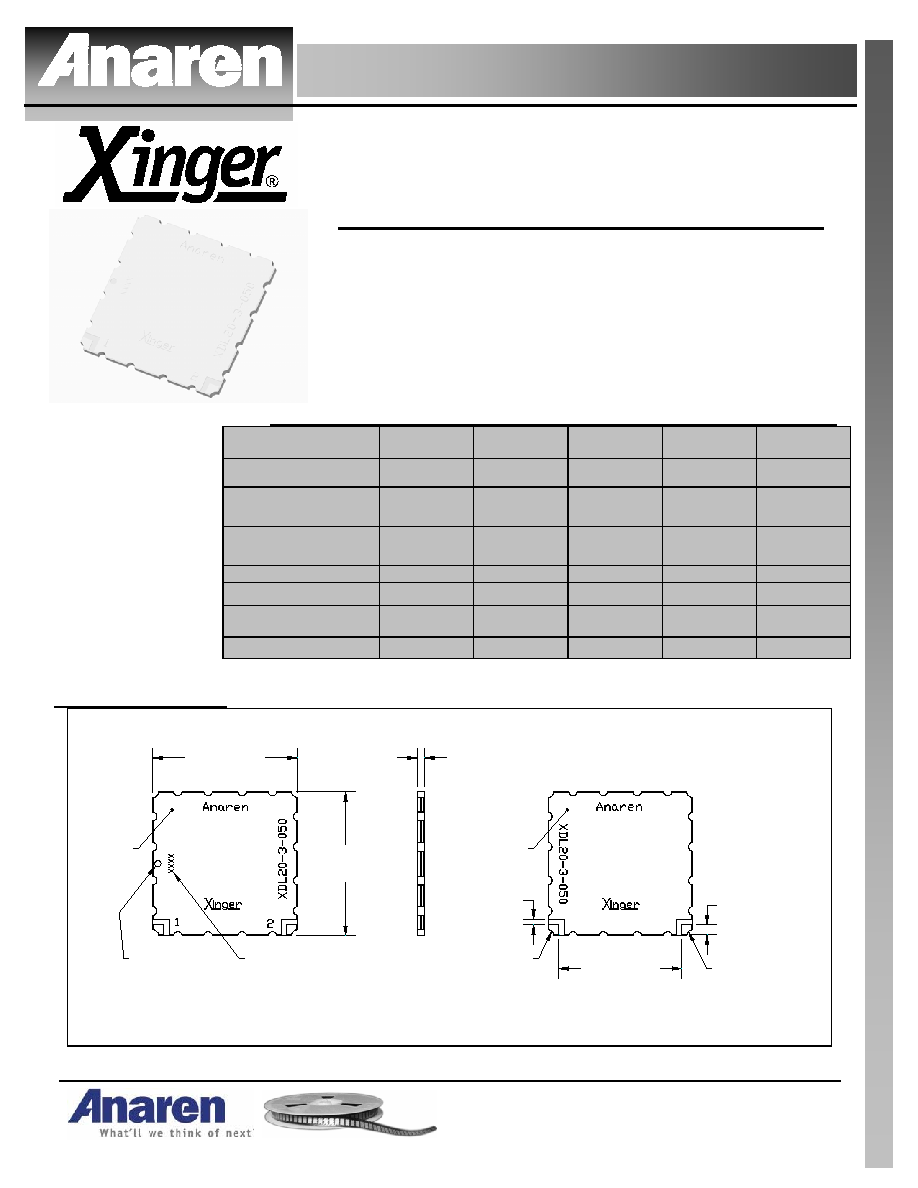
Mechanical Drawing
XDL20-3-050 Rev A Mechanical Outline
Dimensions are in Inches [Millimeters]
.051
±.005
[1.28
±0.13
]
Side View
1.000
±.010
[25.40
±0.25
]
1.000
±.010
[25.40
±0.25
]
Top View (Near-side)
Bottom View (Far-side)
Orientation
Marker Denotes
Pin Location
2X .037
±.004
[0.94
±0.10
]
Denotes
Array Number
Pin 2
Pin 1
GND
GND
.848
±.004
[21.54
±0.10
]
2X .070
±.004
SQ
[1.78
±0.10
]

USA/Canada:
Toll Free:
Europe:
(315) 432-8909
(800) 544-2414
+44 2392-232392
Available on Tape and
Reel For Pick and Place
Manufacturing.
Model XDL20-3-050
Rev. B
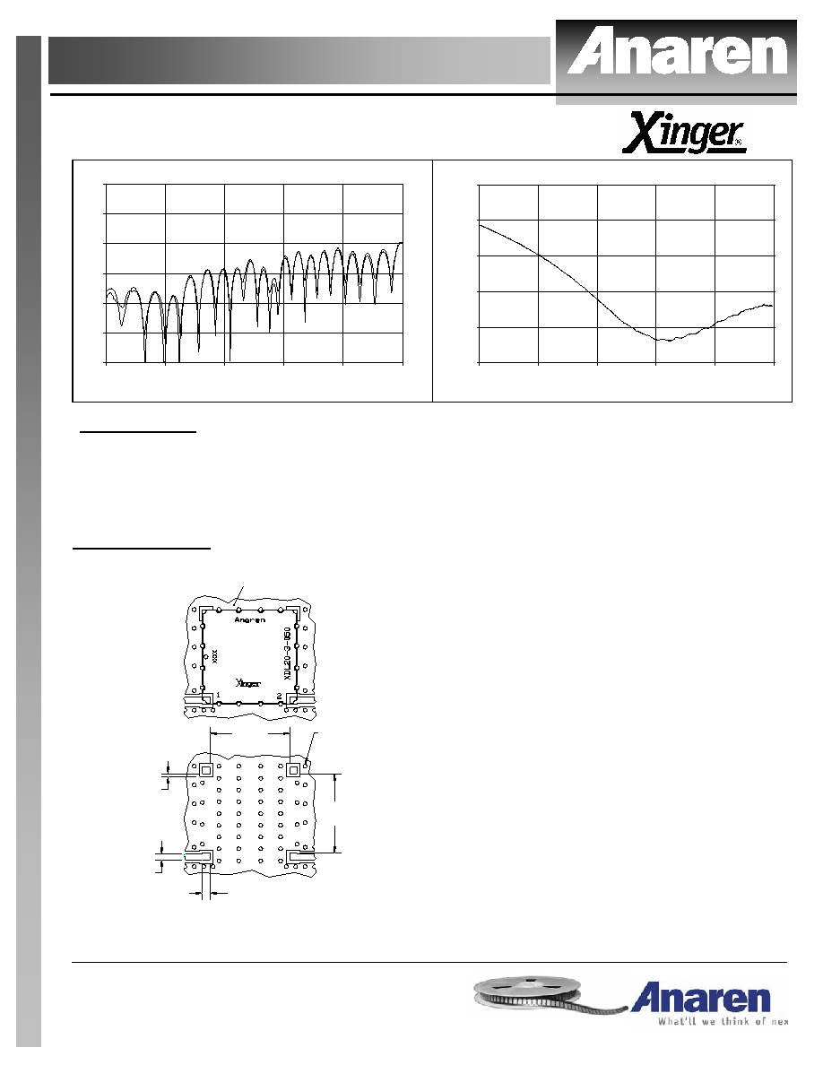
Typical Performance: 0.5GHz. to 3.0GHz.
Return Loss XDL20-3-050
-60
-50
-40
-30
-20
-10
0
500
1000
1500
2000
2500
3000
Frequency [MHz]
R
e
t
u
r
n
L
o
ss
[
d
B
]
Insertion Loss XDL20-3-050
-2.5
-2
-1.5
-1
-0.5
0
500
1000
1500
2000
2500
3000
Frequency [MHz]
I
n
s
e
r
t
ion Los
s
[
d
B
]
AVERAGE DELAY
The average delay is defined as the group delay of the input signal through the delay line. Because the Xinger delay
lines take advantage of a narrow band tuning technique, the average delay over the broad band varies. Because the
XDL20-3-050 is tuned at 2.0GHz, the average delay in that range is larger than at 1.0 GHz and specifications reflects
this variation. The lot-to-lot variation is reflected in the plus/minus tolerance given in specifications.
Refer to Anaren Application Note AAN-232 for further information on Xinger delay lines.
Mounting Guidelines:
XDL20-3-050 Rev A Mounting Footprint
Dimensions are in Inches [Millimeters]
To ensure proper electrical and thermal performance
there must be a ground plane with 100%
solder connection underneath the part
.848
[21.54]
4X .037
[0.94]
Multiple
plated thru holes
to ground
.848
[21.54]
4X .076 SQ
[1.93]
2X 50
Transmission
Line
In order for Xinger surface mount delay lines to work
optimally, there must be 50
transmission lines leading to
and from all of the RF ports. Also, there must be a very
good ground plane under the part with a number of plated
thru holes to ensure proper electrical performance. If any
of these conditions are not satisfied, insertion loss,
average delay and VSWR may not meet published
specifications.
When a surface mount delay line is mounted to a printed
circuit board (PCB), the primary concerns are; insuring
the RF pads of the device are in contact with the circuit
trace of the PCB and the ground plane of neither the
component nor the PCB are in contact with the RF signal.
An example of how
the PCB footprint could look is shown
below. In particular designs, the 50
lines need to be
adjusted to the unique dielectric coefficients and
thicknesses as well as varying pick and place equipment
tolerances.
