Available on Tape
and Reel For Pick and
Place Manufacturing.
USA/Canada:
Toll Free:
Europe
:
(315) 432-8909
(800) 544-2414
+44 2392-232392
Model X2B
Rev. A
SMT Crossover
Description
The X2B is a low profile crossover to intersect an RF and RF circuit trace in
an easy to use surface mount package designed for frequencies up to 6
GHz. The X2B is ideal for any application where an RF circuit must intersect
with another RF circuit without resorting to a multilayer PCB. Parts have
been run through rigorous qualification testing and units are 100% tested.
They are manufactured using materials with x and y thermal expansion
coefficients compatible with common substrates such as FR4, G-10 and
polyamide.
ELECTRICAL
SPECIFICATIONS**
Frequency
Port Impedance
Return Loss
Isolation
GHz
Ohms
dB Min
DB Min
DC � 2.5
50
20
50
2.5 � 4.0
50
20
30
4.0 � 6.0
50
15
20
Insertion Loss
Power
JC
Operating
Temp.
dB Max
Watts
�C / Watt
�C
0.05
30
143.4
-55 to +85
0.10
15
143.4
-55 to +85
Features:
� DC � 6.0 GHz
� RF � RF Crossover
� Low Loss
� High Isolation
� Surface Mountable
� Tape And Reel
� Convenient Package
� 100% Tested
0.15
10
143.4
-55 to +85
**Specification based on performance of unit properly installed on microstrip printed circuit
boards with 50
nominal impedance. Specifications subject to change without notice.
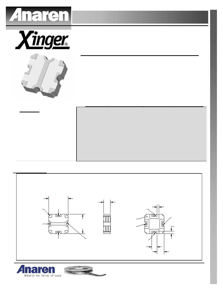
Outline Drawing
X2B Rev A Mechanical Outline
Dimensions are in Inches [Millimeters]
Side View
Bottom View (Far-side)
Top View (Near-side)
.200
�.010
[5.08
�0.25
]
.200
�.010
[5.08
�0.25
]
.071
�.007
[1.80
�0.18
]
.056
�.004
[1.42
�0.10
]
.025
�.008
[0.65
�0.20
]
.020
�.004
TYP
[0.51
�0.10
]
.072
�.008
[1.83
�0.20
]
4X GND
RF IN/OUT
RF IN/OUT
RF IN/OUT
RF IN/OUT
RF IN/OUT
RF IN/OUT
RF IN/OUT
RF IN/OUT
GND

USA/Canada:
Toll Free:
Europe:
(315) 432-8909
(800) 544-2414
+44 2392-232392
Available on Tape and
Reel For Pick and Place
Manufacturing.
Model X2B
Rev. A
Typical Performance: 0 GHz. to 6.0 GHz.
Return Loss X2B
-60
-50
-40
-30
-20
-10
500
1000
1500
2000
2500
3000
3500
4000
4500
5000
5500
6000
Frequency (MHz)
R
e
tu
r
n
L
o
s
s
(
d
B
)
Insertion Loss X2B
-0.50
-0.40
-0.30
-0.20
-0.10
0.00
500
1000
1500
2000
2500
3000
3500
4000
4500
5000
5500
6000
Frequency (MHz)
I
n
ser
t
i
o
n Loss
(
d
B
)
Isolation X2B
-80.00
-70.00
-60.00
-50.00
-40.00
-30.00
-20.00
500
1000
1500
2000
2500
3000
3500
4000
4500
5000
5500
6000
Frequency (MHz)
I
s
ol
at
i
on (
d
B
)
Phase Balance X2B
-6.0
-4.0
-2.0
0.0
2.0
4.0
6.0
500
1000
1500
2000
2500
3000
3500
4000
4500
5000
5500
6000
Frequency (MHz)
P
h
a
s
e B
a
l
anc
e (
D
egr
e
e
s
)
Mounting Mounting
Footprint
In order for Xinger crossovers to work optimally, there must be
50 transmission lines leading to and from all of the RF ports.
Also, there must be a very good ground to the corners of the
crossover to insure proper electrical performance. If either of
these two conditions are not satisfied, insertion loss, VSWR
and isolation parameters may not meet published
specifications.
When a surface mount crossover is mounted to a printed
circuit board, the primary concerns are; insuring the RF pads
of the device are in contact with the circuit trace of the PCB
and insuring the ground plane of neither the component nor
the PCB is in contact with the RF signal. Since the component
is not symmetrical, the crossovers are specifically oriented in
the tape and reel. An example of how the PCB footprint could
look is shown below. In specific designs, the 50 lines need
to be adjusted to the unique dielectric coefficients and
thicknesses as well as varying pick and place equipment
tolerances.
X2B Rev A Mounting Footprint
Dimensions are in Inches [Millimeters]
4X 50
Transmission
Line
.034 TYP
[0.86]
To ensure proper electrical and thermal performance
there must be a ground plane with 100%
solder connection underneath the part
Multiple
plated thru holes
to ground
.063 SQ TYP
[1.60]
.042 TYP
[1.07]
.034 TYP
[0.86]