SmartSwitch
TM
AAT4625
USB Single-Channel Power Switch
Preliminary
Information
4625.2002.1.0.93
1
General Description
The AAT4625
SmartSwitchTM
is
part
of
AnalogicTech's
Application
Specific
Power
MOSFETTM (ASPMTM) product family. It is a 1.0A
Current Limited P-channel, MOSFET power switch
designed for high-side load-switching applications.
This switch operates with inputs ranging from 2.7V
to 5.5V, making it ideal for both 3V and 5V systems.
An integrated current-limiting circuit protects the
input supply against large changes in load current
which may cause the supply to fall out of regulation.
The AAT4625 is also protected from thermal over-
load which limits power dissipation and junction
temperatures. The current limit threshold is factory
programmed at 1.5A, with a maximum of 2.0A. The
quiescent supply current is typically a low 16µA. In
shutdown mode, the supply current decreases to
less than 1µA.
The AAT4625 is available in 8 pin SOP or TSSOP
and is specified over a -40 to 85°C temperature
range.
The AAT4600 Series is a family of adjustable and
fixed SmartSwitchTM products with a range of cur-
rent handling capabilities. Single versions with
adjustable current limit (AAT4601) or fixed current
limit (AAT4625) as well as dual versions with fixed
current limit (AAT4626) are available.
Features
·
Compliant with USB 1.1 and 2.0 specifications
·
2.7V to 5.5V Input voltage range
·
1.0A minimum continuous current
·
2.0A maximum current limit
·
60m
typical R
DS(ON)
·
Low quiescent current
·
Typically 16µA
·
1µA max with Switch off
·
Thermal shutdown
·
Fault flag with 10ms blanking
·
Undervoltage Lockout
·
Temp range -40 to 85°C
·
UL Approved--File No. E217765
·
8 pin SOP or TSSOP package
Applications
·
USB ports and peripherals
·
Notebook computers
·
Hot swap supplies
·
General purpose power switching
UL Recognized Component
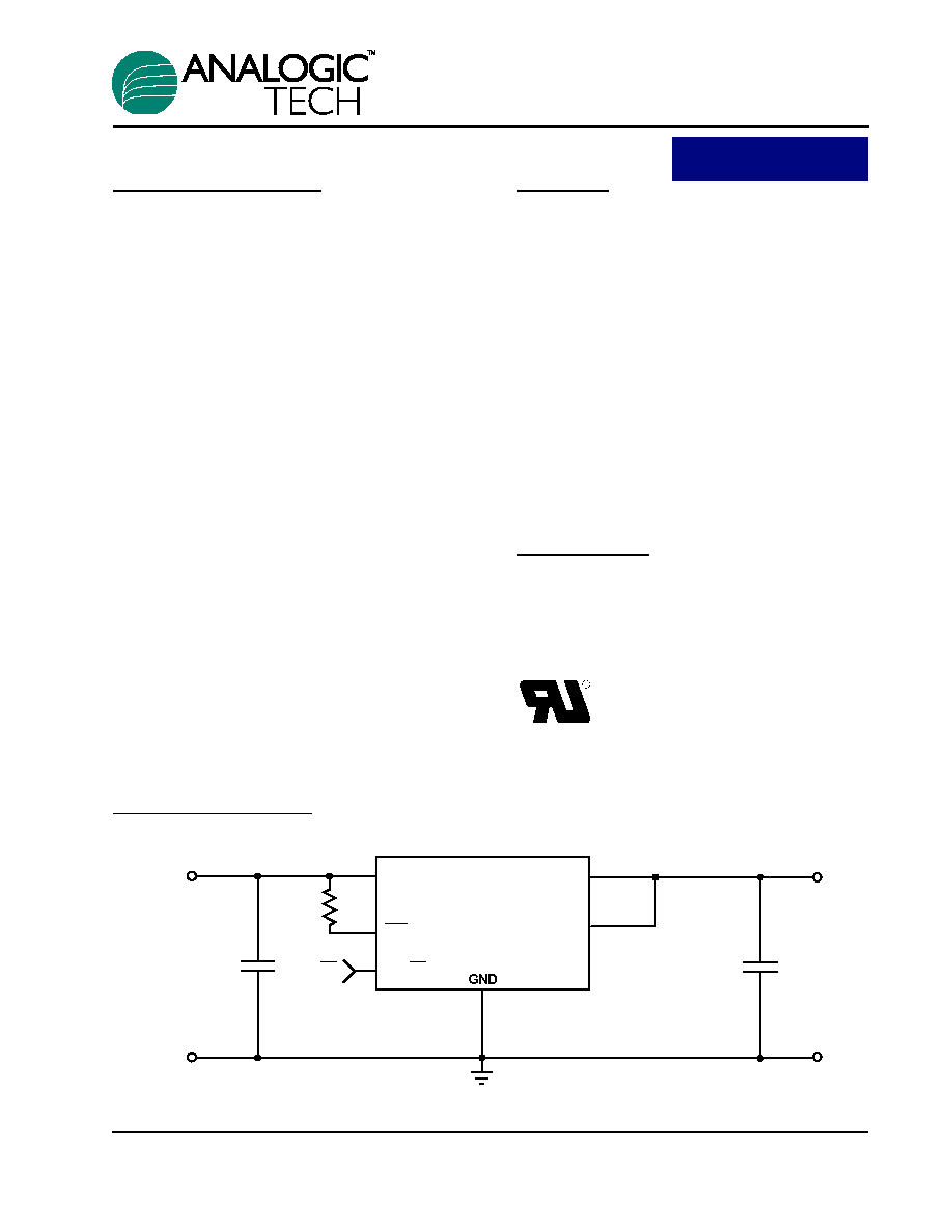
Typical Application
120
µ
F
GND
GND
OUTPUT
OUT
OUT
IN
EN (EN)
EN (EN)
0.1
µ
F
V
CC
5.0V
100k
FLG
7
2
1
3
8
6
AAT4625
Pin Descriptions
Pin Configuration
SOP-8
TSSOP-8
(Top View)
(Top View)
1
2
IN
OUT
OUT
NC
EN (EN)
FLG
GND
NC
1
2
3
4
8
7
6
5
1
2
EN (EN)
FLG
GND
NC
OUT
IN
OUT
NC
Pin #
Symbol
Function
1
EN (EN)
Enable Input: Logic-compatible enable input. High input > 2.1V typical. Low
input < 1.9V typical. Active high or active low option available; see Ordering
Information for details.
2
FLG
Fault Flag Output: Active-low, open-drain output. Indicates over current,
UVLO and thermal shutdown.
3
GND
Ground connection
4,5
NC
Not internally connected.
6,8
OUT
Switch Output: These pins are the P-channel MOSFET drain connection.
7
IN
Supply Input: This pin is the P-channel MOSFET source connection. Also
supplies the IC's internal circuitry.
AAT4625
USB Single-Channel Power Switch
2
4625.2002.1.0.93

Absolute Maximum Ratings
(T
A
=25°C unless otherwise noted)
Note: Stresses above those listed in Absolute Maximum Ratings may cause permanent damage to the device. Functional operation at con-
ditions other than the operating conditions specified is not implied. Only one Absolute Maximum rating should be applied at any one time.
Thermal Information
Note 1: Mounted on an FR4 printed circuit board.
Electrical Characteristics
(V
IN
= 5V, T
A
= -40 to 85°C unless otherwise noted. Typical values
are at T
A
=25°C; bold values designate full temperature range)
Symbol
Description
Conditions
Min
Typ
Max
Units
V
IN
Operation Voltage
2.7
5.5
V
I
Q
Quiescent Current
V
IN
=5V, EN=active
16
30
µA
I
Q(OFF)
Off Supply Current
V
IN
=5.5V, EN (EN)=inactive
1
µA
V
EN-THRSH
Enable Input Threshold
Low-to-high transition
2.4
V
High-to-low transition
0.8
V
I
EN
Enable Input Current
V
EN
= 0V to 5.5V
0.01
1
µA
C
EN
Enable Input Capacitance
1
pF
R
ds(ON)
On-Resistance
V
IN
=5V, T
A
= 25°C
60
100
m
V
IN
=3.0V, T
A
= 25°C
70
115
m
T
ON
Output Turn-On Delay
V
IN
=5V, R
L
=10
0.25
ms
T
ON-RISE
Output Turn-On Rise Time
V
IN
=5V, R
L
=10
0.2
ms
T
OFF
Output Turn-Off Delay
V
IN
=5V, R
L
=10
5
20
µs
T
OFF-FALL
Output Turn-Off Fall Time
V
IN
=5V, R
L
=10
20
µs
I
SD(OFF)
Output Leakage Current
EN=inactive, V
IN
=5.5V, V
OUT
=0V
0.03
15
µA
I
LIMIT
Current Limit Threshold
ramped load applied to enable
1.0
1.5
2.0
A
output, V
OUT
< 4.0V
OTMP
Over Temperature Shut Down
T
J
increasing
125
°C
T
J
decreasing
115
°C
R
FLG
Error Flag Output Resistance
V
IN
=5V, I
L
= 1mA
30
I
SINK
Error Flag Off Current
V
FLG
= 5.5V
0.05
1
µA
V
UVLO
Under voltage Lockout
V
IN
= increasing, 1% hysteresis
2.0
2.3
2.7
V
T
BLANK
FAULT blanking
10
ms
Symbol
Description
Value
Units
JA
Maximum Thermal Resistance (SOP-8)
1
100
°C/W
P
D
Maximum Power Dissipation (SOP-8)
1
1.25
W
Symbol
Description
Value
Units
V
IN
IN to GND
-0.3 to 6
V
V
FLG
FLG to GND
-0.3 to 6
V
I
FLG
FLG Current
50
mA
V
OUT
OUT to GND
-0.3 to V
IN
+0.3
V
I
OUT
Output Current (Internally Limited)
2.0
A
V
EN
EN to GND
-0.3 to 6
V
T
S
Storage Temperature
150
°C
T
LEAD
Maximum Soldering Temperature (at Leads)
300
°C
AAT4625
USB Single-Channel Power Switch
4625.2002.1.0.93
3

Typical Characteristics
(Unless otherwise noted, V
IN
= 5V, T
A
= 25°C)
Turn-ON/OFF Response with 10
Ohm 1
µ
F load
EN (5V/div)
FAULT
Vout (2V/
µ
div)
Iin (200mA/div)
Off-Switch Current vs. Temperature
0.0000
0.0001
0.0010
0.0100
0.1000
1.0000
-40
-20
0
20
40
60
80
100
120
Off-Switch Current (
µ
A)
Off-Supply Current vs. Temperature
0.0010
0.0100
0.1000
1.0000
-40
-20
0
20
40
60
80
100
120
Temperature (
°
C)
Off-Supply Current (
µ
A)
Current Limit
0
0.2
0.4
0.6
0.8
1
1.2
1.4
1.6
1.8
0
1
2
3
4
5
O
Output (A)
utput (V)
Quiescent Current
0
2
4
6
8
10
12
14
16
18
20
0
1
2
3
4
5
6
Input (V)
Input (
µ
A)
Quiescent Current vs. Temperature
0
5
10
15
20
25
30
-40
-20
0
20
40
60
80
100
120
Temp
Q
u
i
escen
t
C
urren
t
(
µ
A)
erature (
°
C)
AAT4625
USB Single-Channel Power Switch
4
4625.2002.1.0.93

(Unless otherwise noted, V
IN
= 5V, T
A
= 25°C)
R
ds(ON)
vs. Temperature
40.0
45.0
50.0
55.0
60.0
65.0
70.0
75.0
80.0
-40
-20
0
20
40
60
80
100
120
Temperature (
°
C)
V
CC
=3V
V
CC
=5V
Short Circuit Through 0.6 Ohm
0
2
4
6
8
-1
0
1
2
3
4
5
Ti
Input and Output (V)
Output (A)
me (
µ
s)
-3
0
3
6
9
Input Voltage
Output Current
Output Voltage
Short Circuit Through 0.3 Ohm
0
2
4
6
8
-1
0
1
2
3
4
5
Tim
Input and Output (V)
Output (A)
e (
µ
s)
-4
0
4
8
12
Input Voltage
Output Current
Output Voltage
Thermal Shutdown Response
50ms/ div
EN (5V/div)
FAULT (5V/div)
Vout (1V/div)
Iin (500mA/div)
Start Into 1 Ohm load
1ms/div
EN (5V/div)
FAULT (5V/div)
Vout (1V/div)
Iin (500mA/div)
AAT4625
USB Single-Channel Power Switch
4625.2002.1.0.93
5

Functional Block Diagram
1.2V
Reference
Current
Limit
Over-Temp
Protection
Under-
voltage
Lockout
IN
EN (EN)
GND
FLG
OUT
AAT4625
USB Single-Channel Power Switch
6
4625.2002.1.0.93

Ordering Information
Package Information
SOP-8
1 2
E
b
e
H
D
A1
A
A2
7 (4x)
c
L
y
Q
Package
Enable
Marking
Part Number
Bulk
Tape and Reel
SOP8
EN (Active-high)
AAT4625IAS-1-B1
AAT4625IAS-1-T1
SOP8
EN (Active-low)
AAT4625IAS-B1
AAT4625IAS-T1
TSSOP8
EN (Active-high)
AAT4625IHS-1-B1
AAT4625IHS-1-T1
TSSOP8
EN (Active-low)
AAT4625IHS-B1
AAT4625IHS-T1
AAT4625
USB Single-Channel Power Switch
4625.2002.1.0.93
7
Dim
Millimeters
Inches
Min
Max
Min
Max
A
1.35
1.75
0.053
0.069
A1
0.10
0.25
0.004
0.010
A2
1.45
0.057
B
0.33
0.51
0.013
0.020
C
0.19
0.25
0.007
0.010
D
4.80
5.00
0.189
0.197
E3.80
4.00
0.150
0.157
e
1.27
0.050
H
5.80
6.20
0.228
0.244
L
0.40
1.27
0.016
0.050
Y
0.00
0.10
0.000
0.004
1
0°
8°
0°
8°
Note:
1. PACKAGE BODY SIZES EXCLUDE MOLD FLASH
PROTRUSIONS OR GATE BURRS.
2. TOLERANCE 0.1000mm (4mil) UNLESS
OTHERWISE SPECIFIED
3. COPLANARITY: 0.1000mm
4. DIMENSION L IS MEASURED IN GAGE PLANE.
5. CONTROLLING DIMENSION IS MILLIMETER;
CONVERTED INCH DIMENSIONS ARE NOT
NECESSARILY EXACT.

TSSOP-8
A1
b
e
E
1 2
A
A2
E1
DETAIL A
R
L1
L
0.20
D
R1
2
E
1
DETAIL A
AAT4625
USB Single-Channel Power Switch
8
4625.2002.1.0.93
Advanced Analogic Technologies, Inc.
1250 Oakmead Parkway, Suite 310, Sunnyvale, CA 94086
Phone (408) 524-9684
Fax (408) 524-9689
Dim
Millimeters
Inches
Min
Max
Min
Max
A
1.05
1.20
0.041
0.047
A1
0.05
0.15
0.002
0.006
A2
-
1.05
-
0.041
b
0.25
0.30
0.010
0.012
c
0.127
0.005
D-8
2.90
3.10
0.114
0.122
D-28
9.60
9.80
0.378
0.386
E4.30
4.50
0.170
0.177
E1
6.20
6.60
0.244
0.260
e
0.65 BSC
0.025 BSC
L
0.50
0.70
0.20
0.028
L1
1.0
0.039
R
0.09
-
0.004
-
R1
0.09
-
0.004
-
1
0°
8°
0°
8°
2
12°