TS3V330
QUAD SPDT WIDE BANDWIDTH VIDEO SWITCH
WITH LOW ON STATE RESISTANCE
SCDS162A MAY 2004 REVISED MAY 2004
1
POST OFFICE BOX 655303
·
DALLAS, TEXAS 75265
D
Low Differential Gain and Phase
(D
G
= 0.82%, D
P
= 0.1 Degree Typ)
D
Wide Bandwidth (BW = 300 MHz Min)
D
Low Crosstalk (X
TALK
= -80 dB Typ)
D
Low Power Consumption
(I
CC
= 3
µ
A Max)
D
Bidirectional Data Flow, With Near-Zero
Propagation Delay
D
Low ON-State Resistance (r
on
= 3
Typ)
D
Rail-to-Rail Switching on Data I/O Ports
(0 to V
CC
)
D
V
CC
Operating Range From 3 V to 3.6 V
D
I
off
Supports Partial-Power-Down Mode
Operation
D
Data and Control Inputs Provide
Undershoot Clamp Diode
D
Latch-Up Performance Exceeds 100 mA Per
JESD 78, Class II
D
ESD Performance Tested Per JESD 22
- 2000-V Human-Body Model
(A114-B, Class II)
- 1000-V Charged-Device Model (C101)
D
Suitable for Both RGB and
Composite-Video Switching
description/ordering information
The TI TS3V330 video switch is a 4-bit 1-of-2 multiplexer/demultiplexer with a single switch-enable (EN) input.
When EN is low, the switch is enabled and the D port is connected to the S port. When EN is high, the switch
is disabled and the high-impedance state exists between the D and S ports. The select (IN) input controls the
data path of the multiplexer/demultiplexer.
ORDERING INFORMATION
TA
PACKAGE
ORDERABLE
PART NUMBER
TOP-SIDE
MARKING
QFN - RGY
Tape and reel
TS3V330RGYR
TF330
SOIC - D
Tube
TS3V330D
TS3V330
SOIC - D
Tape and reel
TS3V330DR
TS3V330
-40
°
C to 85
°
C
SSOP (QSOP) - DBQ
Tape and reel
TS3V330DBQR
TF330
-40 C to 85 C
TSSOP - PW
Tube
TS3V330PW
TF330
TSSOP - PW
Tape and reel
TS3V330PWR
TF330
TVSOP - DGV
Tape and reel
TS3V330DGVR
TF330
Package drawings, standard packing quantities, thermal data, symbolization, and PCB design guidelines
are available at www.ti.com/sc/package.
Copyright
2004, Texas Instruments Incorporated
Please be aware that an important notice concerning availability, standard warranty, and use in critical applications of
Texas Instruments semiconductor products and disclaimers thereto appears at the end of this data sheet.
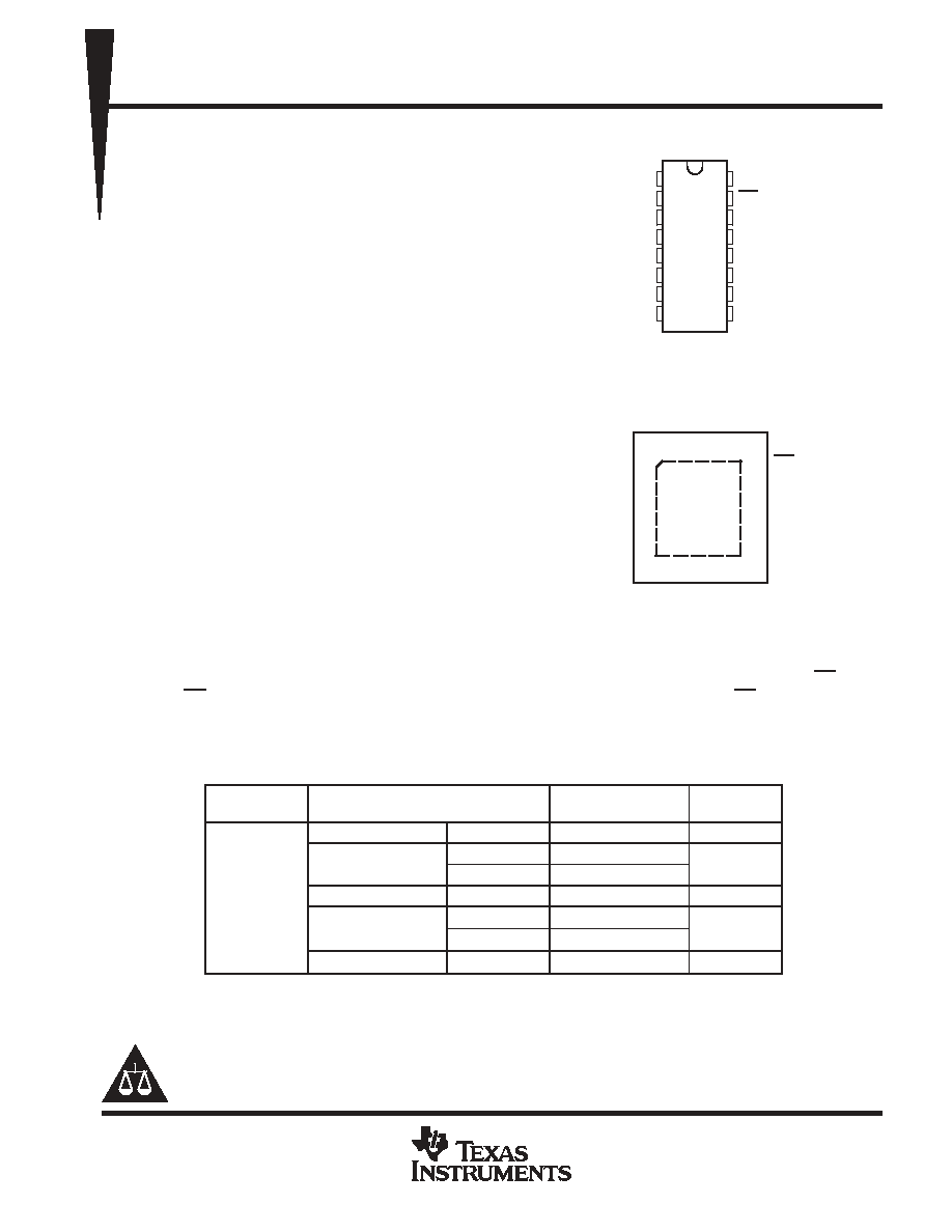
D
D, DBQ, DGV, OR PW PACKAGE
(TOP VIEW)
RGY PACKAGE
(TOP VIEW)
1
16
8
9
2
3
4
5
6
7
15
14
13
12
11
10
EN
S2
D
S2
D
D
D
S1
C
S2
C
S1
A
S2
A
D
A
S1
B
S2
B
D
B
IN
V
GND
CC
1
2
3
4
5
6
7
8
16
15
14
13
12
11
10
9
IN
S1
A
S2
A
D
A
S1
B
S2
B
D
B
GND
V
CC
EN
S1
D
S2
D
D
D
S1
C
S2
C
D
C
C
PRODUCTION DATA information is current as of publication date.
Products conform to specifications per the terms of Texas Instruments
standard warranty. Production processing does not necessarily include
testing of all parameters.
TS3V330
QUAD SPDT WIDE BANDWIDTH VIDEO SWITCH
WITH LOW ON STATE RESISTANCE
SCDS162A MAY 2004 REVISED MAY 2004
2
POST OFFICE BOX 655303
·
DALLAS, TEXAS 75265
description/ordering information (continued)
Low differential gain and phase make this switch ideal for composite and RGB video applications. This device
has wide bandwidth and low crosstalk, making it suitable for high-frequency applications as well.
This device is fully specified for partial-power-down applications using I
off
. The I
off
feature ensures that
damaging current will not backflow through the device when it is powered down. This switch maintains isolation
during power off.
To ensure the high-impedance state during power up or power down, EN should be tied to V
CC
through a pullup
resistor; the minimum value of the resistor is determined by the current-sinking capability of the driver.
FUNCTION TABLE
INPUTS
INPUT/OUTPUT
FUNCTION
EN
IN
INPUT/OUTPUT
D
FUNCTION
L
L
S1
D port = S1 port
L
H
S2
D port = S2 port
H
X
Z
Disconnect
PIN DESCRIPTIONS
PIN NAME
DESCRIPTION
S1, S2
Analog video I/Os
D
Analog video I/Os
IN
Select input
EN
Switch-enable input
TS3V330
QUAD SPDT WIDE BANDWIDTH VIDEO SWITCH
WITH LOW ON STATE RESISTANCE
SCDS162A MAY 2004 REVISED MAY 2004
3
POST OFFICE BOX 655303
·
DALLAS, TEXAS 75265
PARAMETER DEFINITIONS
PARAMETER
DESCRIPTION
RON
Resistance between the D and S ports, with the switch in the ON state
IOZ
Output leakage current measured at the D and S ports, with the switch in the OFF state
IOS
Short-circuit current measured at the I/O pins
VIN
Voltage at the IN pin
VEN
Voltage at the EN pin
CIN
Capacitance at the control (EN, IN) inputs
COFF
Capacitance at the analog I/O port when the switch is OFF
CON
Capacitance at the analog I/O port when the switch is ON
VIH
Minimum input voltage for logic high for the control (EN, IN) inputs
VIL
Minimum input voltage for logic low for the control (EN, IN) inputs
VH
Hysteresis voltage at the control (EN, IN) inputs
VIK
I/O and control (EN, IN) inputs diode clamp voltage
VI
Voltage applied to the D or S pins when D or S is the switch input
VO
Voltage applied to the D or S pins when D or S is the switch output
IIH
Input high leakage current of the control (EN, IN) inputs
IIL
Input low leakage current of the control (EN, IN) inputs
II
Current into the D or S pins when D or S is the switch input
IO
Current into the D or S pins when D or S is the switch output
Ioff
Output leakage current measured at the D or S ports, with VCC = 0
tON
Propagation delay measured between 50% of the digital input to 90% of the analog output when switch is turned ON
tOFF
Propagation delay measured between 50% of the digital input to 90% of the analog output when switch is turned OFF
BW
Frequency response of the switch in the ON state measured at -3 dB
XTALK
Unwanted signal coupled from channel to channel. Measured in -dB. XTALK = 20 log VO/VI. This is a nonadjacent
crosstalk.
OIRR
Off isolation is the resistance (measured in -dB) between the input and output with the switch OFF.
DG
Magnitude variation between analog input and output pins when the switch is ON and the dc offset of composite video
signal varies at the analog input pin. In the NTSC standard, the frequency of the video signal is 3.58 MHz, and dc offset is
from 0 to 0.714 V.
DP
Phase variation between analog input and output pins when the switch is ON and the dc offset of composite-video signal
varies at the analog input pin. In the NTSC standard, the frequency of the video signal is 3.58 MHz, and dc offset is from 0
to 0.714 V.
ICC
Static power-supply current
ICCD
Variation of ICC for a change in frequency in the control (EN, IN) inputs
ICC
This is the increase in supply current for each control input that is at the specified voltage level, rather than VCC or GND.
TS3V330
QUAD SPDT WIDE BANDWIDTH VIDEO SWITCH
WITH LOW ON STATE RESISTANCE
SCDS162A MAY 2004 REVISED MAY 2004
4
POST OFFICE BOX 655303
·
DALLAS, TEXAS 75265
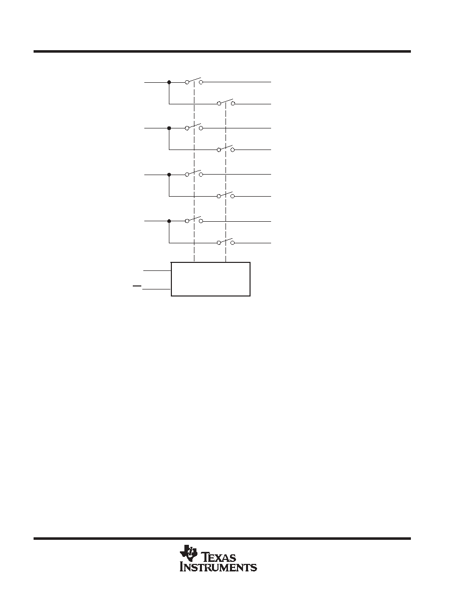
functional diagram (positive logic)
DA
S1A
S2A
S1B
S2B
S1C
S2C
S1D
S2D
EN
IN
DC
DB
DD
4
7
9
12
2
3
5
6
11
10
14
13
15
1
Control
Logic
TS3V330
QUAD SPDT WIDE BANDWIDTH VIDEO SWITCH
WITH LOW ON STATE RESISTANCE
SCDS162A MAY 2004 REVISED MAY 2004
5
POST OFFICE BOX 655303
·
DALLAS, TEXAS 75265
absolute maximum ratings over operating free-air temperature range (unless otherwise noted)
Supply voltage range, V
CC
-0.5 V to 4.6 V
. . . . . . . . . . . . . . . . . . . . . . . . . . . . . . . . . . . . . . . . . . . . . . . . . . . . . . . . .
Control input voltage range, V
IN
(see Notes 1 and 2)
-0.5 V to 4.6 V
. . . . . . . . . . . . . . . . . . . . . . . . . . . . . . . . . .
Switch I/O voltage range, V
I/O
(see Notes 1, 2, and 3)
-0.5 V to 4.6 V
. . . . . . . . . . . . . . . . . . . . . . . . . . . . . . . . .
Control input clamp current, I
IK
(V
IN
< 0)
-50 mA
. . . . . . . . . . . . . . . . . . . . . . . . . . . . . . . . . . . . . . . . . . . . . . . . . . .
I/O port clamp current, I
I/OK
(V
I/O
< 0)
-50 mA
. . . . . . . . . . . . . . . . . . . . . . . . . . . . . . . . . . . . . . . . . . . . . . . . . . . . .
ON-state switch current, I
I/O
(see Note 4)
±
128 mA
. . . . . . . . . . . . . . . . . . . . . . . . . . . . . . . . . . . . . . . . . . . . . . . . .
Continuous current through V
CC
or GND terminals
±
100 mA
. . . . . . . . . . . . . . . . . . . . . . . . . . . . . . . . . . . . . . . . .
Package thermal impedance,
JA
(see Note 5): D package
73
°
C/W
. . . . . . . . . . . . . . . . . . . . . . . . . . . . . . . . . . .
(see Note 5): DBQ package
90
°
C/W
. . . . . . . . . . . . . . . . . . . . . . . . . . . . . . . .
(see Note 5): DGV package
120
°
C/W
. . . . . . . . . . . . . . . . . . . . . . . . . . . . . . .
(see Note 5): PW package
108
°
C/W
. . . . . . . . . . . . . . . . . . . . . . . . . . . . . . . .
(see Note 6): RGY package
39
°
C/W
. . . . . . . . . . . . . . . . . . . . . . . . . . . . . . . .
Storage temperature range, T
stg
-65
°
C to 150
°
C
. . . . . . . . . . . . . . . . . . . . . . . . . . . . . . . . . . . . . . . . . . . . . . . . . . .
Stresses beyond those listed under "absolute maximum ratings" may cause permanent damage to the device. These are stress ratings only, and
functional operation of the device at these or any other conditions beyond those indicated under "recommended operating conditions" is not
implied. Exposure to absolute-maximum-rated conditions for extended periods may affect device reliability.
NOTES:
1. All voltages are with respect to ground, unless otherwise specified.
2. The input and output voltage ratings may be exceeded if the input and output clamp-current ratings are observed.
3. VI and VO are used to denote specific conditions for VI/O.
4. II and IO are used to denote specific conditions for II/O.
5. The package thermal impedance is calculated in accordance with JESD 51-7.
6. The package thermal impedance is calculated in accordance with JESD 51-5.
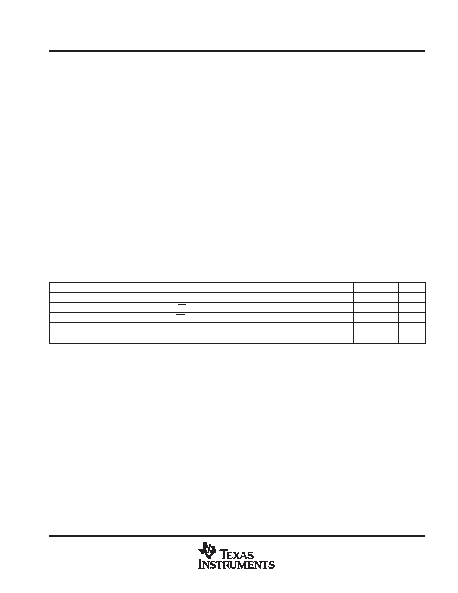
recommended operating conditions (see Note 7)
MIN
MAX
UNIT
VCC
Supply voltage
3
3.6
V
VIH
High-level control input voltage (EN, IN)
2
VCC
V
VIL
Low-level control input voltage (EN, IN)
0
0.8
V
VANALOG
Analog I/O voltage
0
VCC
V
TA
Operating free-air temperature
-40
85
°
C
NOTE 7: All unused control inputs of the device must be held at VCC or GND to ensure proper device operation. Refer to the TI application report,
Implications of Slow or Floating CMOS Inputs, literature number SCBA004.