Äîêóìåíòàöèÿ è îïèñàíèÿ www.docs.chipfind.ru

AD120
Preliminary
3-Level / 258 Outputs TFT LCD Gate Driver
PRELIMINARY (August, 2001, Version 0.0)
AMIC Technology, Inc.
Document Title
3-Level / 258 Outputs TFT LCD Gate Driver
Revision History
Rev. No. History
Issue Date
Remark
0.0
Initial issue
August 10, 2001
Preliminary
Important Notice:
AMIC reserves the right to make changes to its products or to discontinue any integrated circuit product or
service without notice. AMIC integrated circuit products are not designed, intended, authorized, or warranted to
be suitable for use in life-support applications, devices or systems or other critical applications. Use of AMIC
products in such applications is understood to be fully at the risk of the customer.
AD120
Preliminary
3-Level / 258 Outputs TFT LCD Gate Driver
PRELIMINARY (August, 2001, Version 0.0)
1
AMIC Technology, Inc
Features
n
TFT LCD gate driver
n
3-level / 258 outputs
n
40V max. for each output
n
-15V min. for each output
n
2.7V~3.6V logic input/output level
n
Bi-directional data shift control
n
Output waveform control
n
TCP available
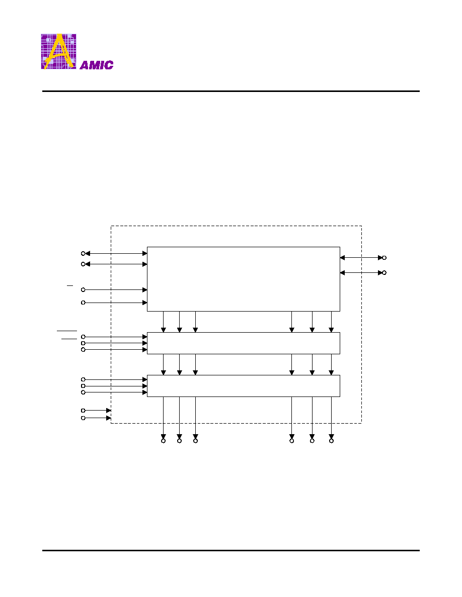
AD120 is a gate driver for TFT LCD panel. There are 258 outputs in the chip. Three-level output allows voltage correction for
better switching noise rejection. It can be used for XGA / SXGA panels.
Block Diagram
Shift Register
Decoder
Output
.........
.........
.........
ST1X
ST2X
.........
ST2
ST1
CP
XOFF
XON
OGW
VH
VOFF
VL
VDD
VSS
OUT0 OUT1 OUT2
OUT255 OUT256 OUT257
R/L
AD120
PRELIMINARY (August, 2001, Version 0.0)
2
AMIC Technology, Inc
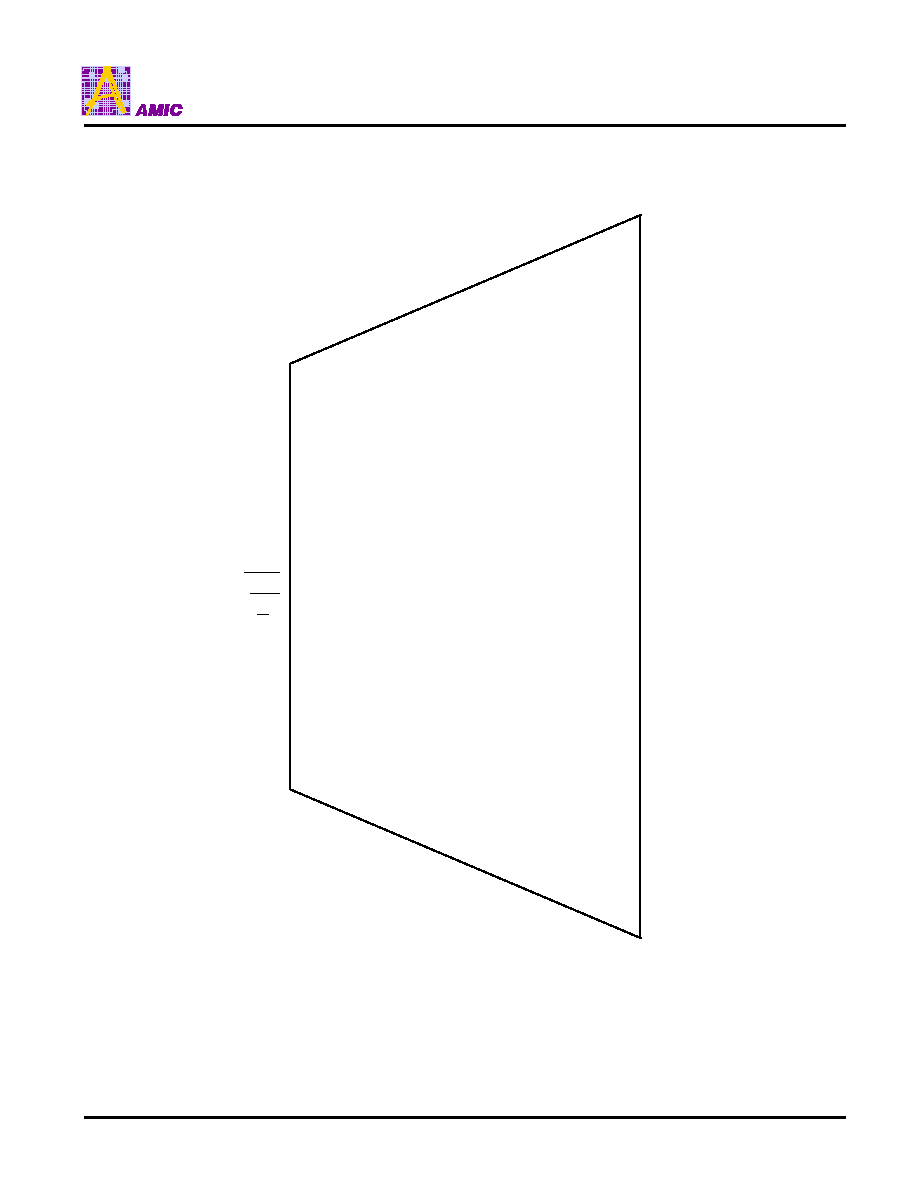
TCP Pinout
1
2
3
4
5
6
7
8
9
10
11
12
13
14
15
16
17
18
19
20
21
22
275
274
273
272
271
......................................................................
OUT254
OUT257
OUT253
OUT255
OUT256
OUT1
OUT4
OUT0
OUT2
OUT3
.......................................................................
VL
VOFF
VH
ST1
ST2
VSS
CP
VDD
XOFF
XON
R/L
OGW
ST2X
ST1X
VH
VOFF
VL
AD120

AD120
PRELIMINARY (August, 2001, Version 0.0)
3
AMIC Technology, Inc
Input/Output Pin Function
Pin No.
Symbol
I/O
Description
11
CP
I
Clock pulse
7
R
/L
I
Right / left direction control for shift register
When
R /L
is LOW, data are shifted to the right, or ST1 / ST2 output0 output1
.... output257.
When R /L
is HIGH, data are shifted to the left, or ST1X / ST2X
output257
output256
.
...
output0.
8
XON
I
XON to
force all the outputs to VH voltage.
It is not synchronous to CP.
9
XOFF
I
XOFF to
force all the outputs to VOFF voltage.
It is not synchronous to CP.
6
OGW
I
Output Gate pulse Width to select output_waveform format.
4,5,
13,14
ST1, ST2,
ST1X, ST2X
I/O
When
R /L
is LOW, ST1 / ST2 are defined as inputs while ST1X / ST2X are defined
as outputs .
The synchronized ST1 / ST2 signals are placed at ST1X / ST2X after 256 CP pulses.
When
R /L
is HIGH, ST1X / ST2X are defined as inputs, while ST1/ST2 are defined
as outputs.
The synchronized ST1X / ST2X signals are placed at ST1 / ST2 after 256 CP pulses.
18 - 275
OUT0~
OUT257
O
Output drivers
These outputs are synchronized to CP pulses.
The output format and voltage level are controlled by OGW,
XON
,
XOFF
, ST1 /
ST2, ST1X / ST2X and
R /L
correspondingly as shown in the diagram.
12
VSS
PWR Reference voltage
10
VDD
PWR Supply voltage for logic operation
VDD and VSS are voltage levels of input / output logic signals
3, 15
VH
PWR High voltage for output drivers
1, 17
VL
PWR Low voltage for output drivers
2, 16
VOFF
PWR OFF voltage for output drivers
AD120
PRELIMINARY (August, 2001, Version 0.0)
4
AMIC Technology, Inc
Description
Operation
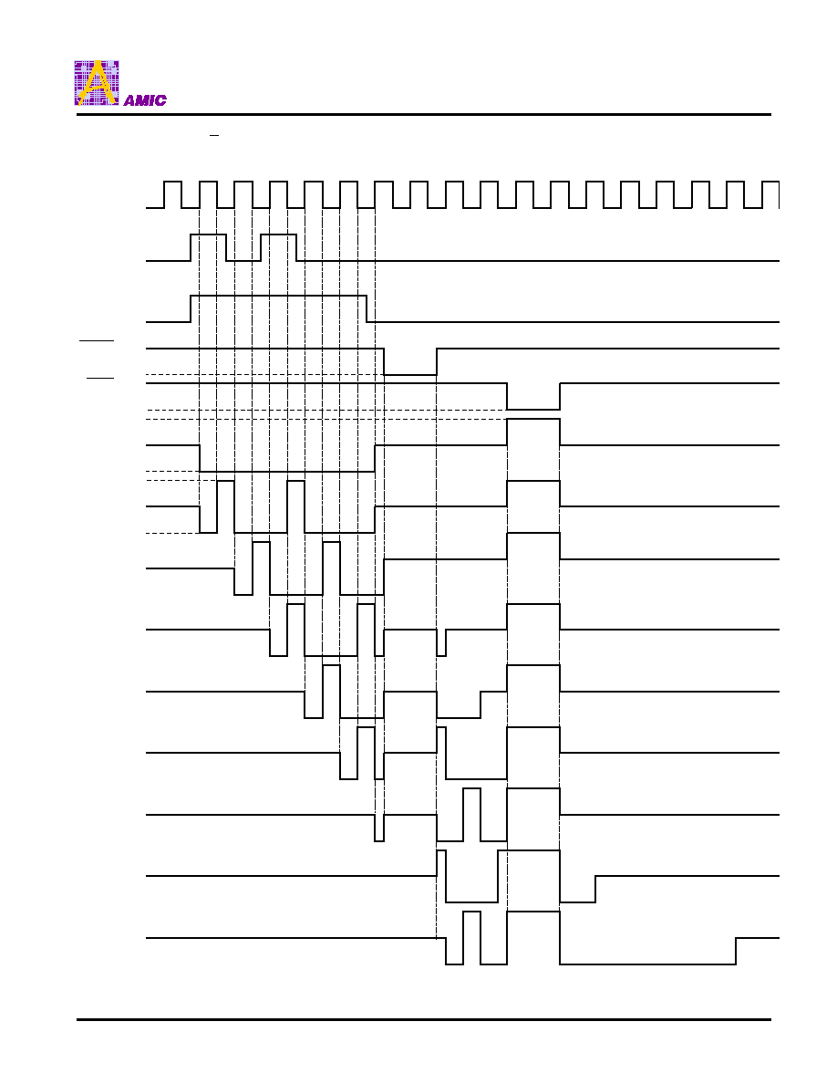
Output signals OUT0~OUT257 are used for control of the TFT gates of the LCD panel. A bi-directional shift register is
implemented to sequentially output signals OUT0~OUT257. A clock pulse CP is applied to the bi-directional shift register and
the direction of the register is controlled by
R /L
signal.
When
R /L
is LOW and either starting signal ST1 or ST2 goes to HIGH, the shift register starts shifting from OUT0 to OUT257.
The voltages of the corresponding outputs switch to VH, VL or VOFF depending on the starting signals as shown in the
diagram. The outputs of the starting signals ST1X / ST2X switch accordingly after 256 CP pulses following start of the shift
register which allows expansion of the outputs by cascading more devices.
When
R /L
is HIGH and either starting signal ST1X or ST2X goes to HIGH, the shift register starts shifting from OUT257 to
OUT0. The voltages of the corresponding outputs switch to VH, VL or VOFF depending on the starting signals as shown in the
diagram. The outputs of the starting signals ST1/ST2 switch accordingly after 256 CP pulses following start of the shift register
which allows expansion of the outputs by cascading more devices.
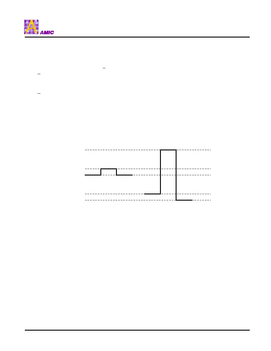
3-Level Output
V
H
- V
L
= 40V(max.)
V
OFF
- V
L
= 0~10V
V
H
- V
SS
= 17~28V
OUT
Level
V
H
V
DD
V
SS
V
OFF
V
L
AD120
PRELIMINARY (August, 2001, Version 0.0)
5
AMIC Technology, Inc
Operation Diagram 1 (
R
/L = L, OGW = L)
~ ~
~ ~
~ ~
~ ~
~ ~
~ ~
~ ~
~ ~
~ ~
~ ~
CP
ST1
ST2
OUT0
OUT1
OUT2
OUT3
OUT256
OUT257
ST1X
ST2X
V
H
V
OFF
V
L
V
H
V
OFF
V
L
V
H
V
OFF
V
L
V
H
V
OFF
V
L
V
H
V
OFF
V
L
V
H
V
OFF
V
L
1
2
3
256
257
V
DD
V
SS
V
DD
V
SS
V
DD
V
SS
V
DD
V
SS
AD120
PRELIMINARY (August, 2001, Version 0.0)
6
AMIC Technology, Inc
Operation Diagram 2 (
R
/L = L, OGW = H)
CP
ST1
ST2
1
2
3
XON
OUT0
OUT1
OUT2
OUT3
OUT4
OUT5
OUT6
OUT7
OUT8
V
DD
V
SS
XOFF
V
DD
V
SS
V
H
V
OFF
V
L
V
H
V
OFF
V
L
AD120
PRELIMINARY (August, 2001, Version 0.0)
7
AMIC Technology, Inc
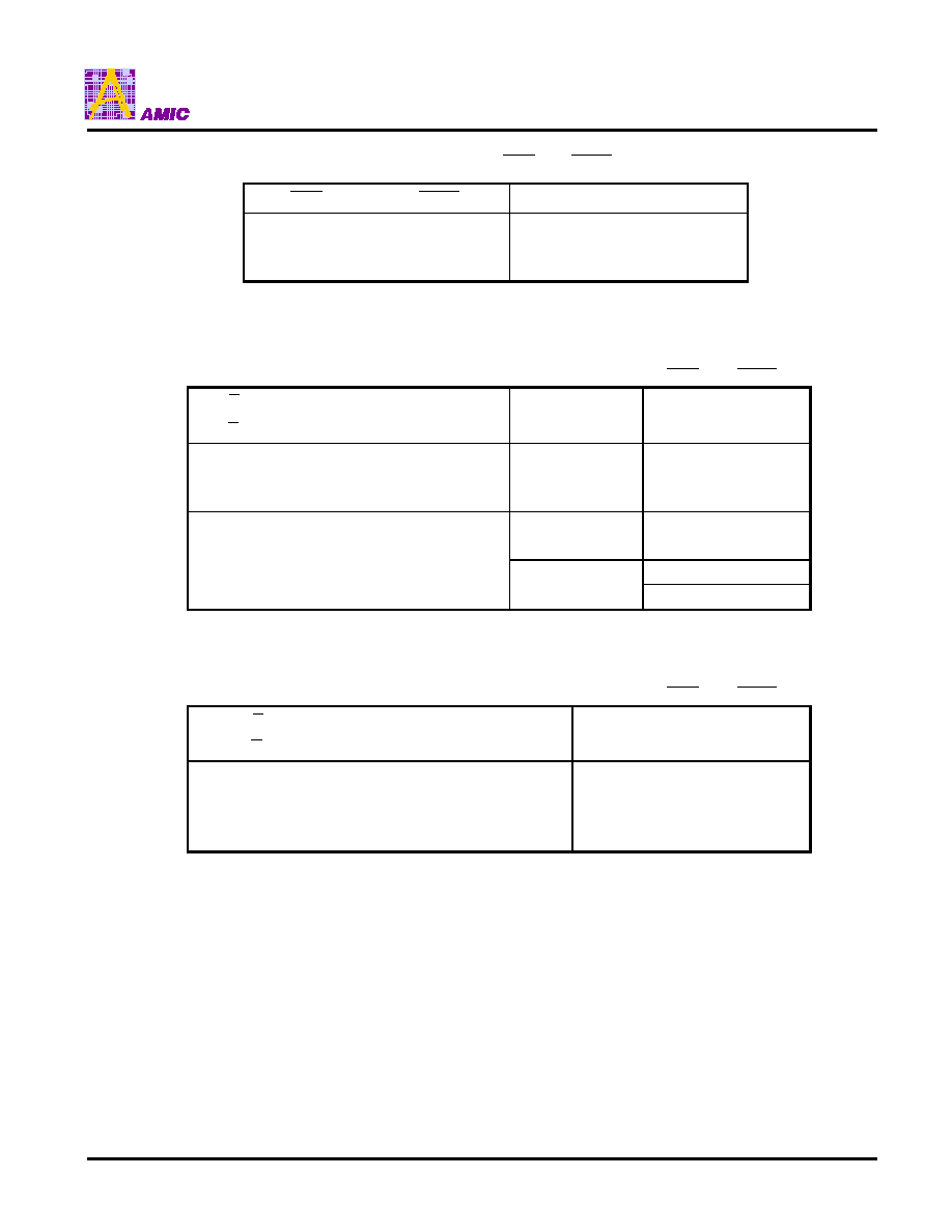
Table 1. Function of XON
and
XOFF
XON
XOFF
OUT0~OUT257
L
X
VH
H
L
VOFF
H
H
Table2
* The outputs are asynchronous to CP.
Table 2. Control of OUT1~OUT256
( XON
= H,
XOFF
= H)
(
R
/L = L) ST1
ST2
(
R
/L = H) ST1X
ST2X
OGW
OUT1~OUT256
L
L
X
VOFF
L
H
X
VL
H
L
X
VL
L
VH
VH (CP = "L")
H
H
H
VL (CP = "H")
* The outputs are synchronous to CP.
Table 3. Control of OUT0 and OUT257
( XON
= H,
XOFF
= H)
(
R
/L = L) ST1
ST2
OUT0
(
R
/L = H) ST1X
ST2X
OUT257
L
L
VOFF
L
H
VL
H
L
VL
H
H
VL
* The outputs are synchronous to CP.
AD120
PRELIMINARY (August, 2001, Version 0.0)
8
AMIC Technology, Inc
Absolute Maximum Ratings Over Operating Free-air Temperature Range
Parameter
Symbol
Ratings
Unit
Supply Voltage
VDD
-0.3 ~ +7.0
V
Supply Voltage
VH
-0.3 ~ 42.0
V
Supply Voltage
VL
-20.0 ~ +0.3
V
Supply Voltage
VOFF
VL-0.3 ~ VL+11.0
V
Supply Voltage
VH - VL
-0.3 ~ 42.0
V
Input Voltage
VIN
-0.3 ~ VDD+0.3
V
Storage Temperature
Tstg
-55 ~ 125
°C
Power_on Sequence and Voltage Levels
V
H
V
OFF
V
L
V
DD
V
SS
V
DD
Logic Signal
V
SS
Out0~Out257
Operating Voltage Range
Parameter
Symbol
Min.
Typ.
Max.
Unit
Supply Voltage
V
DD
2.7
3.3
3.6
V
Supply Voltage
V
H
17
-
28
V
Supply Voltage
V
L
-15
-
-5
V
Supply Voltage
V
OFF
- V
L
0
-
10.0
V
Supply Voltage
V
H
- V
L
22
-
40
V
Clock Frequency
f
CP
-
-
100
KHz
Operating Free-air Temperature
Ta
-20
-
+75
°C
AD120
PRELIMINARY (August, 2001, Version 0.0)
9
AMIC Technology, Inc
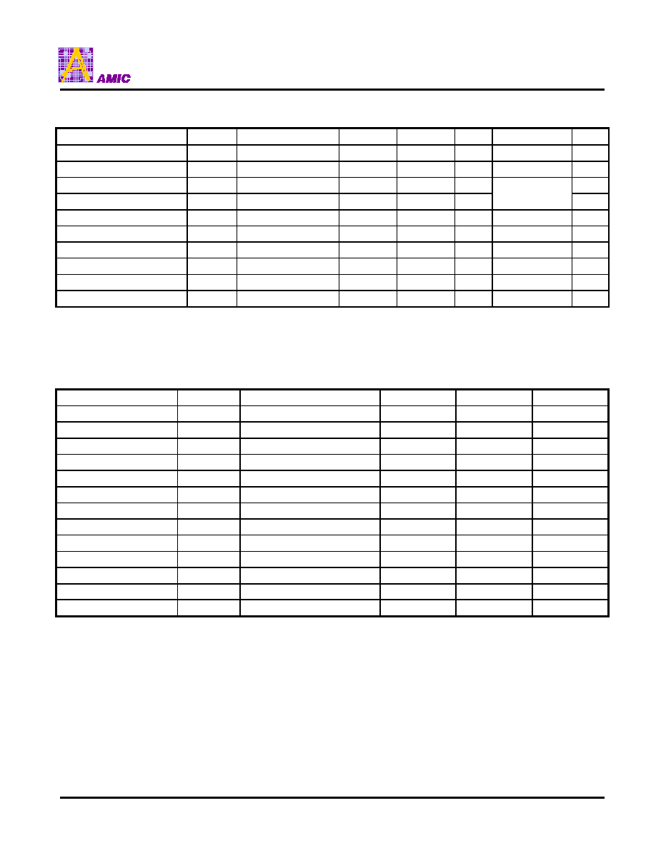
DC Charactertics
(VDD = 2.7~3.6V, Ta = -20~75°C)
Parameter
Symbol
Condition
Min.
Max.
Unit
Applicable Pin
Note
Low Level Input Voltage
V
IL
VSS
0.2 X VDD
V
All input pins
High Level Input Voltage
V
IH
0.8 X VDD
VDD
V
All input pins
Low Level Output Voltage
V
OL
I
OL
= 40µA
VSS
VSS + 0.4
V
High Level Output Voltage
V
OH
I
OH
= 40µA
VDD -0.4
VDD
V
ST1, ST2,
ST1X, ST2X
Output Resistance (1)
R
L
V
OUT
= V
L
+ 0.5
1000
Ù
OUT0~OUT257
1
Output Resistance (2)
R
OFF
V
OUT
= V
OFF
+ 0.5
1000
Ù
OUT0~OUT257
1
Output Resistance (3)
R
H
V
OUT
= V
H
- 0.5
1000
Ù
OUT0~OUT257
1
Input Current
I
I
V
I
= VDD / VSS
-5.0
+5.0
µA
All input pins
Operating Current (1)
I
DD
1500
µA
VDD
1, 2
Operating Current (2)
I
H
100
µA
VH
1, 2
Notes:
1. V
H
= 25V, V
OFF
= 0V, V
L
= -10V
2. CP = 50KHz
AC Charactertics
(VDD = 2.7~3.6V, Ta = -20~75°C)
Parameter
Symbol
Condition
Min.
Max.
Unit
Clock Frequency
f
CP
100
KHz
CP High Pulse Width
t
CPH
1
µs
CP Low Pulse Width
t
CPL
4
µs
Input Rise Time
tr
10% ~ 90%
50
ns
Input Fall Time
tf
90% ~ 10%
50
ns
Gate Off Time
t
WOFF
1
µs
Data Setup Time
t
SU
700
ns
Data Hold Time
thd
700
ns
Delay Time 1
tpd1
CL = 20pF
800
ns
Delay Time 2
tpd2
CL = 300pF
1000
ns
Delay Time 3
tpd3
CL = 300pF
1000
ns
Delay Time 4
tpd4
CL = 300pF
1000
ns
Delay Time 5
tpd5
CL = 300pF
1000
ns
AD120
PRELIMINARY (August, 2001, Version 0.0)
10
AMIC Technology, Inc
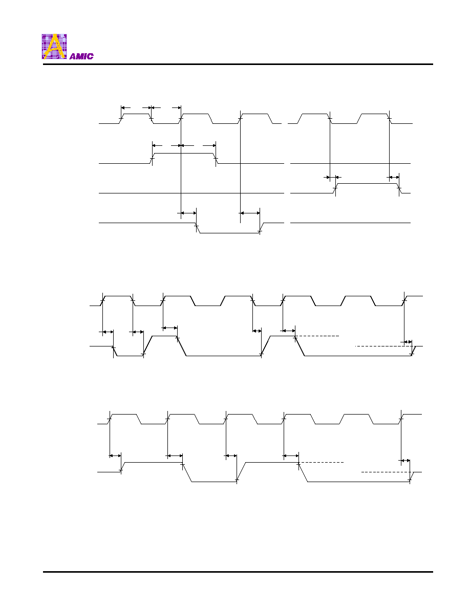
Timing Waveform
------------------------------------------------------------------------------------------------------------------------------------------------------------------------
(OGW = H)
CP
0.5 x V
DD
0.5 x V
DD
0.5 x V
DD
0.5 x V
DD
0.5 x V
DD
OUT0~257
tpd2
tpd2
80%
20%
20%
20%
80%
80%
tpd2
tpd2
tpd2
tpd2
V
H
V
OFF
V
L
0.5 x V
DD
------------------------------------------------------------------------------------------------------------------------------------------------------------------------
(OGW = L)
CP
0.5 x V
DD
0.5 x V
DD
0.5 x V
DD
0.5 x V
DD
20%
0.5 x V
DD
OUT0~OUT257
tpd2
tpd2
tpd2
tpd2
tpd2
80%
20%
80%
20%
V
H
V
OFF
V
L
CP
ST1,
ST2
STX1,
STX2
OUT0~OUT257
~ ~
~ ~
~ ~
~ ~
t
CPH
t
CPL
0.5 x V
DD
0.5 x V
DD
0.5 x V
DD
1
2
256
0.5 x V
DD
0.5 x V
DD
257
0.5 x V
DD
t
SU
thd
0.5 x V
DD
0.5 x V
DD
tpd1
tpd1
tpd2
tpd2
80%
20%
50%
50%
Input
Output
AD120
PRELIMINARY (August, 2001, Version 0.0)
11
AMIC Technology, Inc
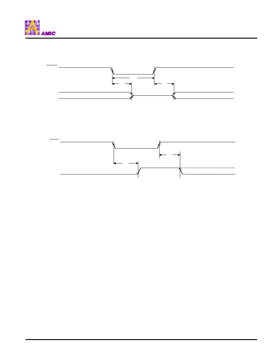
Timing Waveform (continued)
XOFF
0.5 x V
DD
OUT0~OUT257
0.5 x V
DD
V
OFF
tw
OFF
tpd3
tpd3
V
H
V
L
80%
80%
20%
20%
------------------------------------------------------------------------------------------------------------------------------------------------------------------------
XON
0.5 x V
DD
OUT0~OUT257
0.5 x V
DD
tpd4
80%
V
H
20%
tpd4

AD120
PRELIMINARY (August, 2001, Version 0.0)
12
AMIC Technology, Inc
Ordering Information
Part No.
Package
AD120T
TCP