ASM1817
Alliance Semiconductor
2575 Augustine Drive . Santa Clara, CA 95054 . Tel: 408.855.4900 . Fax: 408.855.4999 . www.alsc.com
Notice: The information in this document is subject to change without notice
rev 1.5
Low Power, 3.3V/3.0V µP Reset, Active HIGH, Push-Pull Output
February 2005
General Description
The ASM1817 voltage supervisory device with low-power, 3.3V/
3.0V µP Reset, active HIGH, Push-Pull output. Maximum
supply current over temperature is a low 15µA (at 3.6V).
The ASM1817 generates an active HIGH reset signal whenever
the monitored supply is out of tolerance. A precision reference
and comparator circuit monitor power supply (V
CC
)
level.
Tolerance level options are 5%, 10% and 20% percent. When
an out-of-tolerance condition is detected, an internal power-fail
signal is generated which forces an active HIGH reset signal.
After V
CC
returns to an in-tolerance condition, the reset signal
remains active for 150ms to allow the power supply and system
microprocessor to stabilize.
The ASM1817 is designed with a push-pull output stage and
operates over the extended industrial temperature range.
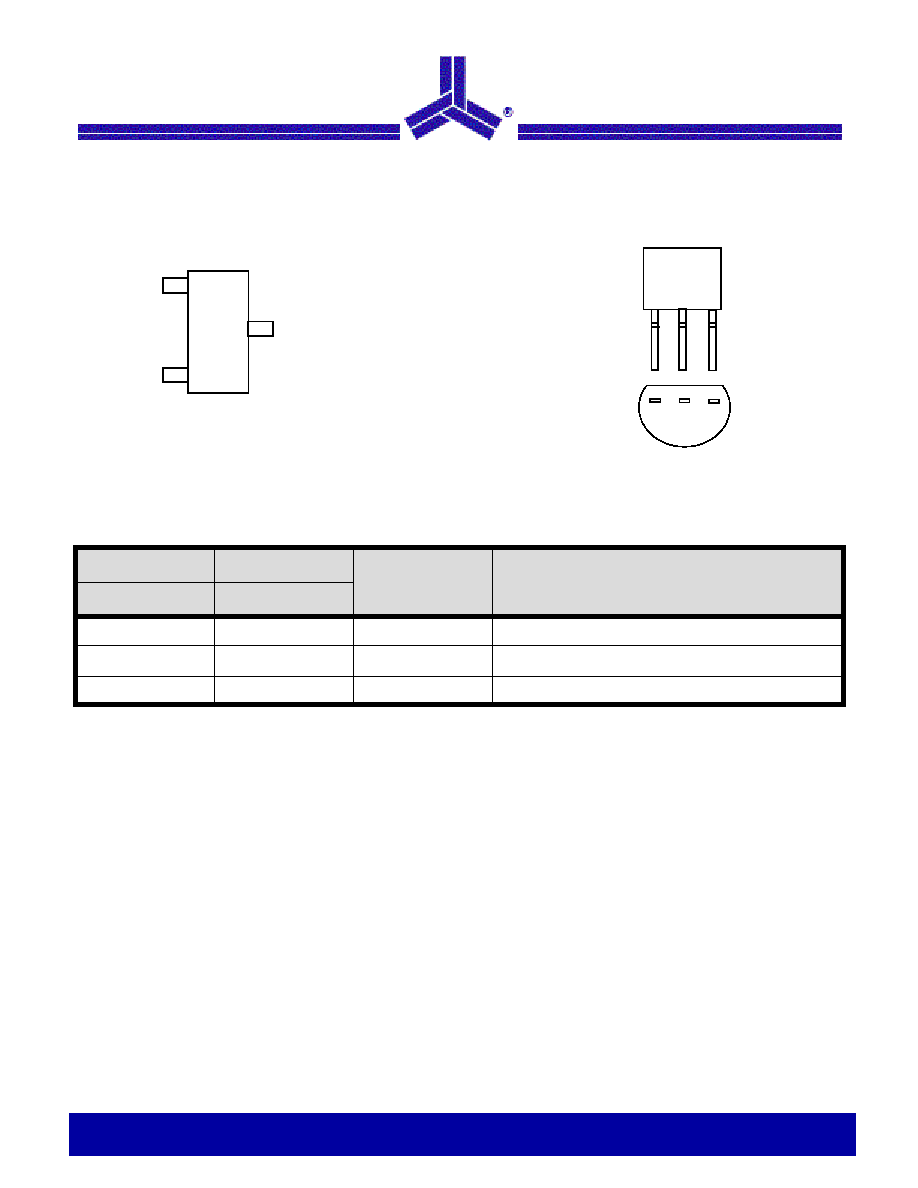
Devices are available in TO-92 and compact surface mount
SOT-23 packages.
Other low power products in this family include the ASM1810/
11/12/15/16, ASM1233D and ASM1233M.
Key Features
·
Low Supply Current
·20 µA maximum (5.5 V)
·15 µA maximum (3.6 V)
·
Automatically restarts a microprocessor after power failure
·
150ms reset delay after V
CC
returns to an in-tolerance con-
dition
·
Active HIGH power-up reset
·
Precision temperature-compensated voltage reference and
comparator
·
Eliminates external components
·
TO-92 and compact surface mount SOT-23 package
·
Push-Pull output for minimum current drain
·
Operating temperature -40°C to +85°C
Applications
·
Set-top boxes
·
Cellular phones
·
PDAs
·
Energy management systems
·
Embedded control systems
·
Printers
·
Single board computers
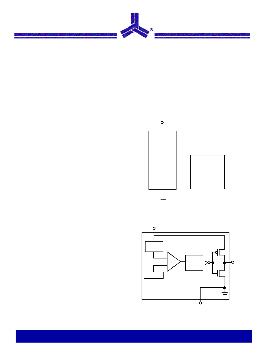
Typical Operating Circuit
Block Diagram
Microprocessor
V
CC
RESET
RESET
GND
ASM1817
ASM1817
V
CC
Supply
Reference
Delay
150ms
Typical
Tolerance
Bias
+
-
V
CC
Supply
Tolerance
Bias
-
GND
RESET
Reference
+
3 of 9
Notice: The information in this document is subject to change without notice
Low Power, 3.3V/3.0V µP Reset
ASM1817
rev 1.5
February 2005
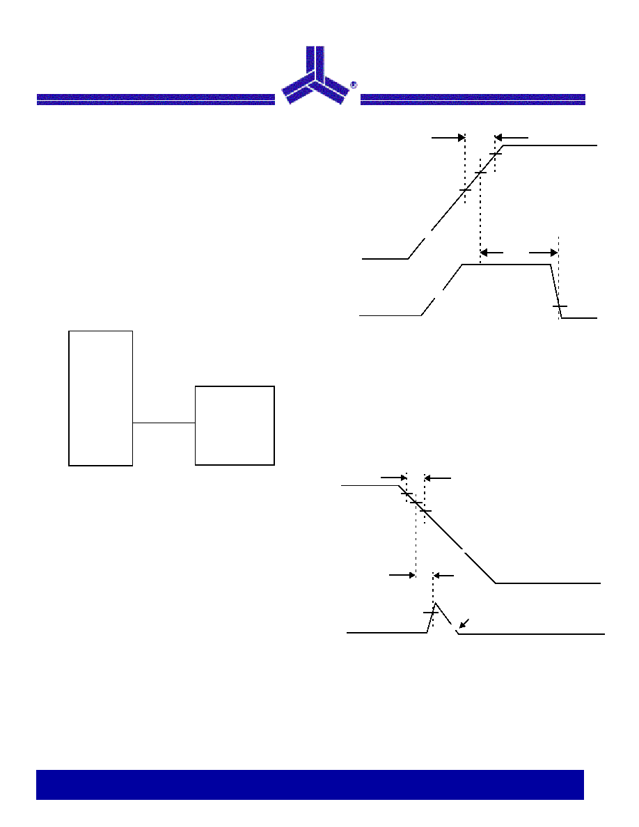
Application Information
Operation - Power Monitor
The ASM1817 detects out-of-tolerance power supply
conditions. It resets a processor during power-up, power-
down and issues a reset to the system processor when the
monitored power supply voltage is below the reset threshold.
When an out-of-tolerance V
CC
voltage is detected, the
RESET signal is asserted. On power-up, RESET is kept
active (HIGH) for approximatley 150ms after the power
supply voltage has reached the selected tolerance. This
allows the power supply and microprocessor to stablize
before RESET is released.
Figure 1: Typical Application
Microprocessor
RESET
RESET
ASM1817
~~
t
RPU
V
CCTP
(MIN)
~ ~
V
CCTP
V
CCTP
(MAX)
t
R
V
CC
Figure 2: Timing Diagram: Power-Up
V
OL
RESET
~ ~
~ ~
t
RPD
V
CC
V
CCTP
(MAX)
V
CCTP
V
CCTP
(MIN)
tF
RESET
RESET Slews with V
CC
V
OH
Figure 3: Timing Diagram: Power-Down
ASM1817
4 of 9
Notice: The information in this document is subject to change without notice
Low Power, 3.3V/3.0V µP Reset
rev 1.5
February 2005
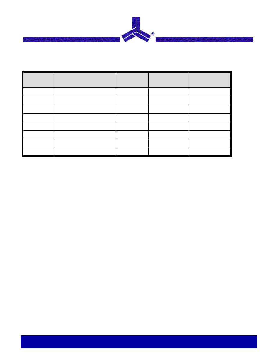
Absolute Maximum Ratings
Electrical Characteristics
Unless otherwise noted, V
CC
= 1.2V to 5.5V and specifications are over the operating temperature range of -40°C to +85°C. All voltages
are referenced to
ground
Parameter
Min
Max
Unit
Voltage on V
CC
-0.5
7
V
Voltage on RESET
-0.5
V
CC
+ 0.5
V
Operating Temperature Range
-40
85
°C
Soldering Temperature (for 10 sec)
260
°C
Storage Temperature
-55
125
°C
ESD rating
HBM
MM
2
200
KV
V
NOTE: These are stress ratings only and functional use is not implied. Exposure to absolute maximum rat-
ings for prolonged periods of time may affect device reliability.
Parameter
Symbol
Conditions
Min
Typ
Max
Unit
Supply voltage
V
CC
1.2
5.5
V
Output Voltage
V
OH
I
OUT
< 500 µA
V
CC
- 0.5V
V
CC
- 0.1V
V
Output Current
I
OH
Output = 2.4V, V
CC
> 2.7V
350
µA
Output Current
I
OL
Output = 0.4V, V
CC
> 2.7V
+10
mA
Operating Current
I
CC
V
CC
< 5.5V, RESET output open
8
20
µA
Operating Current
I
CC
V
CC
< 3.6V, RESET output open
6
15
µA
V
CC
Trip Point (ASM1817R-5)
V
CCTP
2.98
3.06
3.15
V
V
CC
Trip Point (ASM1817R-10)
V
CCTP
2.80
2.88
2.97
V
V
CC
Trip Point (ASM1817R-20)
V
CCTP
2.47
2.55
2.64
V
Output Capacitance
C
OUT
10
pF
V
CC
Detect to RESET Low
t
RPD
2
5
µs
V
CC
Slew Rate
(V
CCTP
(MAX) to V
CCTP
(MIN)
t
F
300
µs
V
CC
Slew Rate
(V
CCTP
(MIN) to V
CCTP
(MAX)
t
R
0
ns
V
CC
Detect to RESET High
t
RPU
t
r
= 5µs
100
150
250
ms
Note: The t
F
value is for reference in defining values for t
RPD
and should not be considered for proper operation or use.