December 2004
Copyright ˋ Alliance Semiconductor. All rights reserved.
Û
AS7C251MNTF18A
12/23/04, v 1.1
Alliance Semiconductor
P. 1 of 18
2.5V 1M x 18 Flowthrough Synchronous SRAM with NTD
TM
Features
ñ Organization: 1,048,576 words æ 18 bits
ñ NTD
TM
architecture for efficient bus operation
ñ Fast clock to data access: 7.5/8.5/10 ns
ñ Fast OE access time: 3.5/4.0 ns
ñ Fully synchronous operation
ñ Flow-through mode
ñ Asynchronous output enable control
ñ Available in 100-pin TQFP package
ñ Individual byte write and global write
ñ Clock enable for operation hold
ñ Multiple chip enables for easy expansion
ñ 2.5V core power supply
ñ Self-timed write cycles
ñ Interleaved or linear burst modes
ñ Snooze mode for standby operation
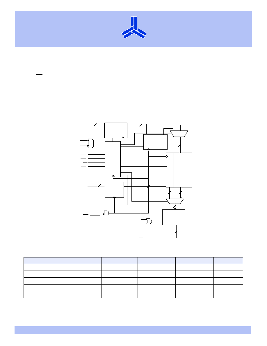
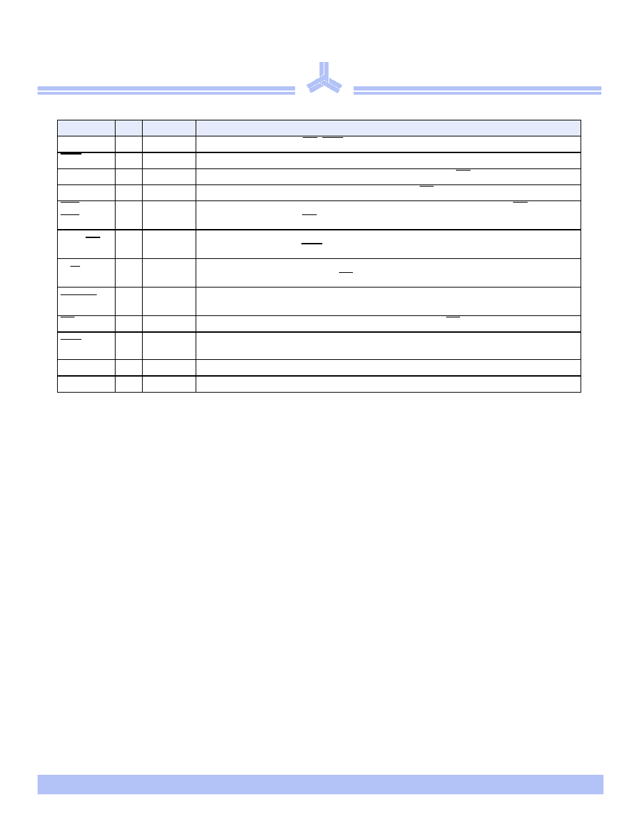
Logic block diagram
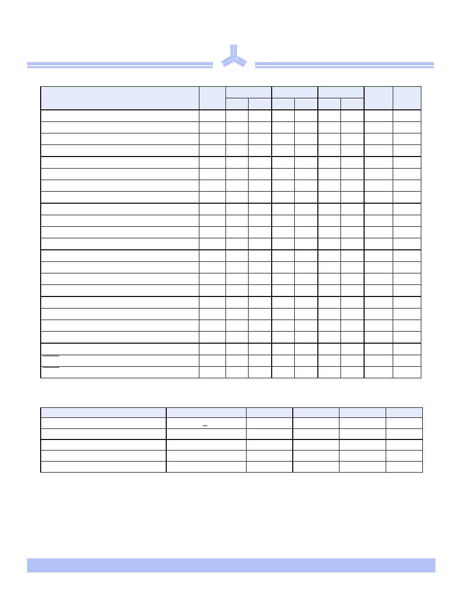
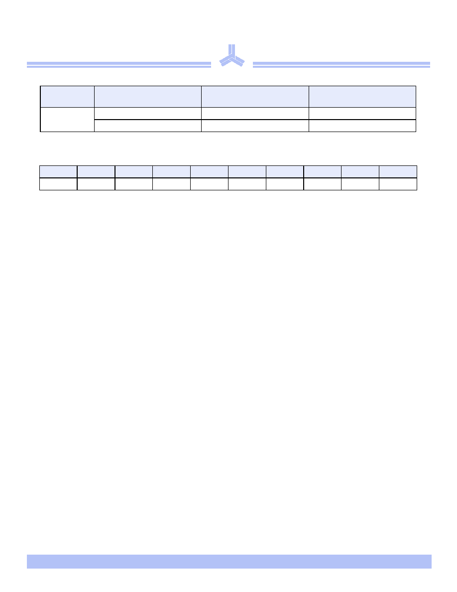
Selection guide
-75
-85
-10
Units
Minimum cycle time
8.5
10
12
ns
Maximum clock access time
7.5
8.5
10
ns
Maximum operating current
275
250
230
mA
Maximum standby current
90
80
80
mA
Maximum CMOS standby current (DC)
60
60
60
mA
W
r
it
e Buf
f
er
Address
D
Q
CLK
register
Output
buffer
DQ [a,b]
20
20
CLK
CE0
CE1
CE2
A[19:0]
OE
CEN
Control
CLK
logic
Data
D
Q
CLK
input
register
18
18
OE
1M x 18
SRAM
array
R/W
DQ [a,b]
BWa
BWb
CLK
Q
D
ADV / LD
LBO
burst logic
addr. registers
Write delay
20
ZZ
CLK
18
18
18
18
Û
AS7C251MNTF18A
12/23/04, v 1.1
Alliance Semiconductor
P. 2 of 18
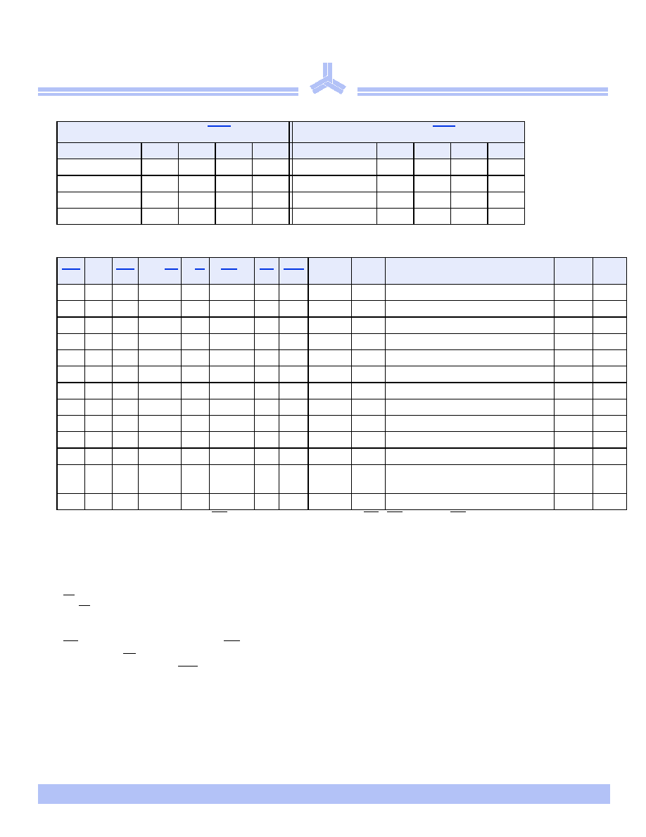
16 Mb 2.5V Synchronous SRAM products list
1,2
1 Core Power Supply: VDD = 2.5V + 0.125V
2 I/O Supply Voltage: VDDQ = 2.5V + 0.125V
PL-SCD
:
Pipelined Burst Synchronous SRAM - Single Cycle Deselect
PL-DCD
:
Pipelined Burst Synchronous SRAM - Double Cycle Deselect
FT
:
Flow-through Burst Synchronous SRAM
NTD
1
-PL
:
Pipelined Burst Synchronous SRAM with NTD
TM
NTD-FT
:
Flow-through Burst Synchronous SRAM with NTD
TM
Org
Part Number
Mode
Speed
1MX18
AS7C251MPFS18A
PL-SCD
166/133 MHz
512KX32
AS7C25512PFS32A
PL-SCD
166/133 MHz
512KX36
AS7C25512PFS36A
PL-SCD
166/133 MHz
1MX18
AS7C251MPFD18A
PL-DCD
166/133 MHz
512KX32
AS7C25512PFD32A
PL-DCD
166/133 MHz
512KX36
AS7C25512PFD36A
PL-DCD
166/133 MHz
1MX18
AS7C251MFT18A
FT
7.5/8.5/10 ns
512KX32
AS7C25512FT32A
FT
7.5/8.5/10 ns
512KX36
AS7C25512FT36A
FT
7.5/8.5/10 ns
1MX18
AS7C251MNTD18A
NTD-PL
166/133 MHz
512KX32
AS7C25512NTD32A
NTD-PL
166/133 MHz
512KX36
AS7C25512NTD36A
NTD-PL
166/133 MHz
1MX18
AS7C251MNTF18A
NTD-FT
7.5/8.5/10 ns
512KX32
AS7C25512NTF32A
NTD-FT
7.5/8.5/10 ns
512KX36
AS7C25512NTF36A
NTD-FT
7.5/8.5/10 ns
1. NTD: No Turnaround Delay. NTD
TM
is a trademark of Alliance Semiconductor Corporation. All trademarks mentioned in this document are the property
of their respective owners.
Û
AS7C251MNTF18A
12/23/04, v 1.1
Alliance Semiconductor
P. 3 of 18
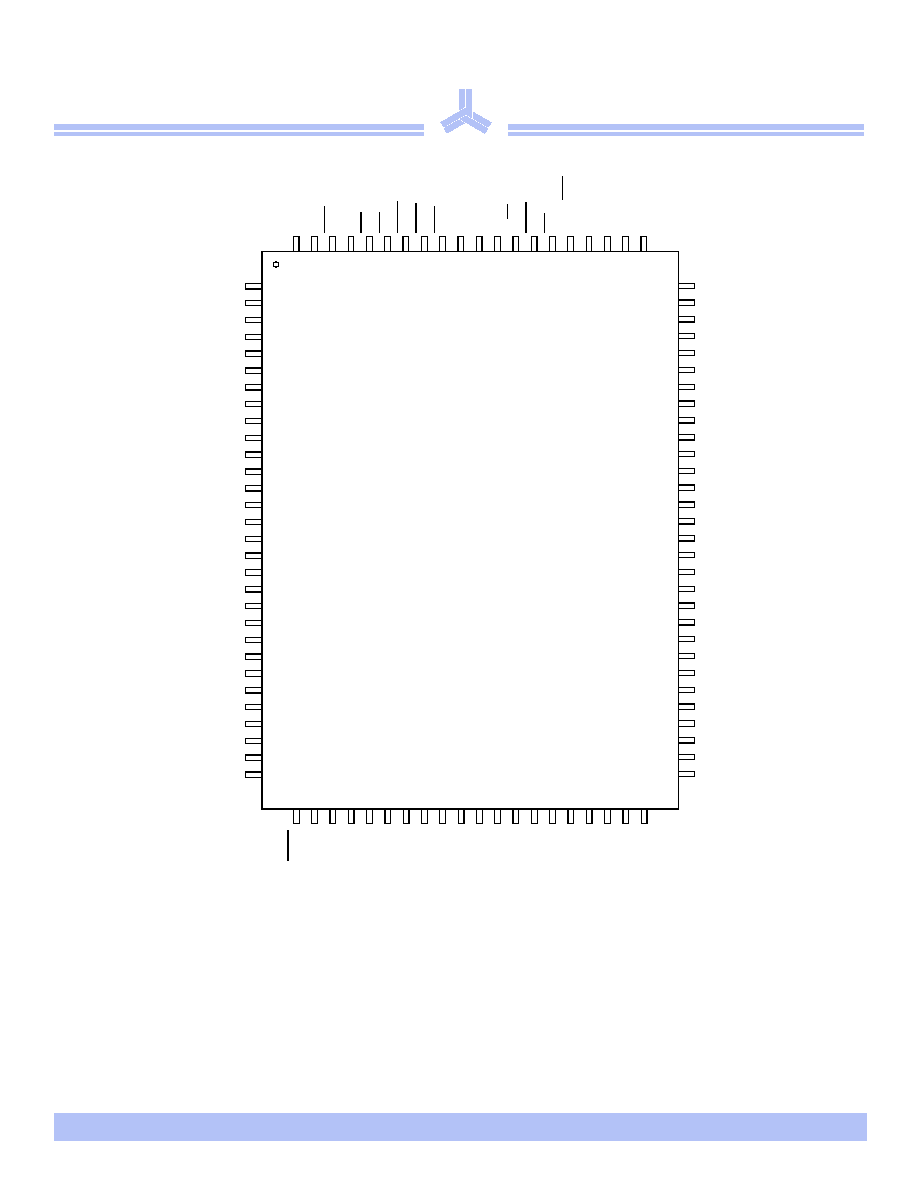
100-pin TQFP - top view
1
2
3
4
5
6
7
8
9
10
11
12
13
14
15
16
17
18
19
20
21
22
23
24
25
26
27
28
29
30
80
79
78
77
76
75
74
73
72
71
70
69
68
67
66
65
64
63
62
61
60
59
58
57
56
55
54
53
52
51
LBO
A
A
A
A
A1
A0
NC
NC
V
SS
V
DD
NC
NC
A
A
A
A
A
A
31
32
33
34
35
36
37
38
39
40
41
42
43
44
45
46
47
48
49
50
10
0
99
98
97
96
95
94
93
92
91
90
89
88
87
86
85
84
83
82
81
A A
CE0
CE1
NC
NC
BW
b
BW
a
CE2
V
DD
V
SS
CLK
R/W
CEN
OE
ADV
/
L
D
A
A
A
A
TQFP 14 x 20mm
A
NC
NC
NC
V
DDQ
V
SSQ
NC
NC
DQb0
DQb1
V
SSQ
V
DDQ
DQb2
DQb3
NC
V
DD
NC
V
SS
DQb4
DQb5
V
DDQ
V
SSQ
DQb6
DQb7
DQPb
NC
V
SSQ
V
DDQ
NC
NC
NC
A
NC
NC
V
DDQ
V
SSQ
NC
DQPa
DQa7
DQa6
V
SSQ
V
DDQ
DQa5
DQa4
V
SS
ZZ
DQa3
DQa2
V
DDQ
V
SSQ
DQa1
DQa0
NC
NC
V
SSQ
V
DDQ
NC
NC
NC
V
DD
NC
Û
AS7C251MNTF18A
12/23/04, v 1.1
Alliance Semiconductor
P. 4 of 18
Functional Description
The AS7C251MNTF18A family is a high performance CMOS 16 Mbit synchronous Static Random Access Memory (SRAM)
organized as 1,048,576 words æ 18 bits and incorporates a LATE Write.
This variation of the 16Mb+ synchronous SRAM uses the No Turnaround Delay (NTD
TM
) architecture, featuring an enhanced
write operation that improves bandwidth over flowthrough burst devices. In a normal flowthrough burst device, the write data,
command, and address are all applied to the device on the same clock edge. If a read command follows this write command,
the system must wait for one 'dead' cycle for valid data to become available. This dead cycle can significantly reduce overall
bandwidth for applications requiring random access or read-modify-write operations.
NTD
TM
devices use the memory bus more efficiently by introducing a write latency which matches the one-cycle flow-
through read latency. Write data is applied one cycle after the write command and address, allowing the read pipeline to clear.
With NTD
TM
, write and read operations can be used in any order without producing dead bus cycle.
Assert R/W low to perform write cycles. Byte write enable controls write access to specific bytes, or can be tied low for full 18
bit writes. Write enable signals, along with the write address, are registered on a rising edge of the clock. Write data is applied
to the device one clock cycle later. Unlike some asynchronous SRAMs, output enable OE does not need to be toggled for write
operations; it can be tied low for normal operations. Outputs go to a high impedance state when the device is de-selected by
any of the three chip enable inputs.
Use the ADV (burst advance) input to perform burst read, write and deselect operations. When ADV is high, external addresses, chip
select, R/W pins are ignored, and internal address counters increment in the count sequence specified by the LBO control. Any
device operations, including burst, can be stalled using the CEN=1, the clock enable input.
The AS7C251MNTF18A operates with a 2.5V Ý 5% power supply for the device core (V
DD
). DQ circuits use a separate
power supply (V
DDQ
). These devices are available in a 100-pin TQFP package.
TQFP capacitance
* Guaranteed not tested
TQFP thermal resistance
Parameter
Symbol
Test conditions
Min
Max
Unit
Input capacitance
C
IN
*
V
IN
= 0V
-
5
pF
I/O capacitance
C
I/O
*
V
OUT
= 0V
-
7
pF
Description
Conditions
Symbol
Typical
Units
Thermal resistance
(junction to ambient)
1
1 This parameter is sampled
Test conditions follow standard test methods
and procedures for measuring thermal
impedance, per EIA/JESD51
1Ùlayer
JA
40
¯C/W
4Ùlayer
JA
22
¯C/W
Thermal resistance
(junction to top of case)
1
JC
8
¯C/W
Û
AS7C251MNTF18A
12/23/04, v 1.1
Alliance Semiconductor
P. 5 of 18
Signal descriptions
Snooze Mode
SNOOZE MODE is a low current, power-down mode in which the device is deselected and current is reduced to I
SB2
. The duration of
SNOOZE MODE is dictated by the length of time the ZZ is in a High state.
The ZZ pin is an asynchronous, active high input that causes the device to enter SNOOZE MODE.
When the ZZ pin becomes a logic High, I
SB2
is guaranteed after the time t
ZZI
is met. After entering SNOOZE MODE, all inputs except ZZ
is disabled and all outputs go to High-Z. Any operation pending when entering SNOOZE MODE is not guaranteed to successfully complete.
Therefore, SNOOZE MODE (READ or WRITE) must not be initiated until valid pending operations are completed. Similarly, when exiting
SNOOZE MODE during t
PUS
, only a DESELECT or READ cycle should be given while the SRAM is transitioning out of SNOOZE MODE.
Signal
I/O Properties
Description
CLK
I
CLOCK
Clock. All inputs except OE, LBO, and ZZ are synchronous to this clock.
CEN
I
SYNC
Clock enable. When de-asserted high, the clock input signal is masked.
A, A0, A1
I
SYNC
Address. Sampled when all chip enables are active and ADV/LD is asserted.
DQ[a,b]
I/O
SYNC
Data. Driven as output when the chip is enabled and OE is active.
CE0, CE1,
CE2
I
SYNC
Synchronous chip enables. Sampled at the rising edge of CLK, when ADV/LD is asserted.
Are ignored when ADV/LD is high.
ADV/LD
I
SYNC
Advance or Load. When sampled high, the internal burst address counter will increment in
the order defined by the LBO input value. When low, a new address is loaded.
R/W
I
SYNC
A high during LOAD initiates a READ operation. A low during LOAD initiates a WRITE
operation. Is ignored when ADV/LD is high.
BW[a,b]
I
SYNC
Byte write enables. Used to control write on individual bytes. Sampled along with WRITE
command and BURST WRITE.
OE
I
ASYNC
Asynchronous output enable. I/O pins are not driven when OE is inactive.
LBO
I
STATIC
Selects Burst mode. When tied to V
DD
or left floating, device follows interleaved Burst order. When
driven Low, device follows linear Burst order. This signal is internally pulled High.
ZZ
I
ASYNC
Snooze. Places device in low power mode; data is retained. Connect to GND if unused.
NC
-
-
No connect
Û
AS7C251MNTF18A
12/23/04, v 1.1
Alliance Semiconductor
P. 6 of 18
Burst order
Synchronous truth table
[5,6,7,8,9,11]
Key: X = Don't Care, H = HIGH, L = LOW.
BWn = H means all byte write signals (BWa, BWb
) are HIGH.
BW
n = L means one or more byte write
signals are LOW.
Notes:
1 CONTINUE BURST cycles, whether READ or WRITE, use the same control inputs. The type of cycle performed (READ or WRITE) is chose in the initial
BEGIN BURST cycle. A CONINUE DESELECT cycle can only be entered if a DESELECT CYCLE is executed first.
2 DUMMY READ and WRITE ABORT cycles can be considered NOPs because the device performs no external operation. A WRITE ABORT means a
WRITE command is given, but no operation is performed.
3 OE may be wired LOW to minimize the number of control signal to the SRAM. The device will automatically turn off the output drivers during a WRITE
cycle. OE may be used when the bus turn-on and turn-off times do not meet an application's requirements.
4 If an INHIBIT CLOCK command occurs during a READ operation, the DQ bus will remain active (Low-Z). If it occurs during a WRITE cycle, the bus will
remain in High-Z. No WRITE operations will be performed during the INHIBIT CLOCK cycle.
5
BW
a enables WRITEs to byte "a" (DQa pins);
BW
b enables WRITEs to byte "b" (DQb pins).
6 All inputs except
OE
and ZZ must meet setup and hold times around the rising edge (LOW to HIGH) of CLK.
7 Wait states are inserted by setting
CEN
HIGH.
8 This device contains circuitry that will ensure that the outputs will be in High-Z during power-up.
9 The device incorporates a 2-bit burst counter. Address wraps to the initial address every fourth BURST CYCLE.
10 The address counter is incremented for all CONTINUE BURST cycles.
11 ZZ pin is always Low in this truth table.
Interleaved burst order (LBO = 1)
Linear burst order (LBO = 0)
A1A0 A1A0 A1A0 A1A0
A1A0 A1A0 A1A0 A1A0
Starting address
0 0
0 1
1 0
1 1
Starting Address
0 0
0 1
1 0
1 1
First increment
0 1
0 0
1 1
1 0
First increment
0 1
1 0
1 1
0 0
Second increment
1 0
1 1
0 0
0 1
Second increment
1 0
1 1
0 0
0 1
Third increment
1 1
1 0
0 1
0 0
Third increment
1 1
0 0
0 1
1 0
CE0 CE1 CE2 ADV/LD R/W
BWn
OE CEN
Address
source
CLK
Operation
DQ
Notes
H
X
X
L
X
X
X
L
NA
L to H
DESELECT Cycle
High-Z
X
X
H
L
X
X
X
L
NA
L to H
DESELECT Cycle
High-Z
X
L
X
L
X
X
X
L
NA
L to H
DESELECT Cycle
High-Z
X
X
X
H
X
X
X
L
NA
L to H
CONTINUE DESELECT Cycle
High-Z
1
L
H
L
L
H
X
L
L
External L to H
READ Cycle (Begin Burst)
Q
X
X
X
H
X
X
L
L
Next
L to H
READ Cycle (Continue Burst)
Q
1,10
L
H
L
L
H
X
H
L
External L to H NOP/DUMMY READ (Begin Burst) High-Z
2
X
X
X
H
X
X
H
L
Next
L to H
DUMMY READ (Continue Burst)
High-Z 1,2,10
L
H
L
L
L
L
X
L
External L to H
WRITE CYCLE (Begin Burst)
D
3
X
X
X
H
X
L
X
L
Next
L to H
WRITE CYCLE (Continue Burst)
D
1,3,10
L
H
L
L
L
H
X
L
External L to H NOP/WRITE ABORT (Begin Burst) High-Z
2,3
X
X
X
H
X
H
X
L
Next
L to H
WRITE ABORT (Continue Burst)
High-Z
1,2,3,
10
X
X
X
X
X
X
X
H
Current L to H
INHIBIT CLOCK
-
4
Û
AS7C251MNTF18A
12/23/04, v 1.1
Alliance Semiconductor
P. 7 of 18
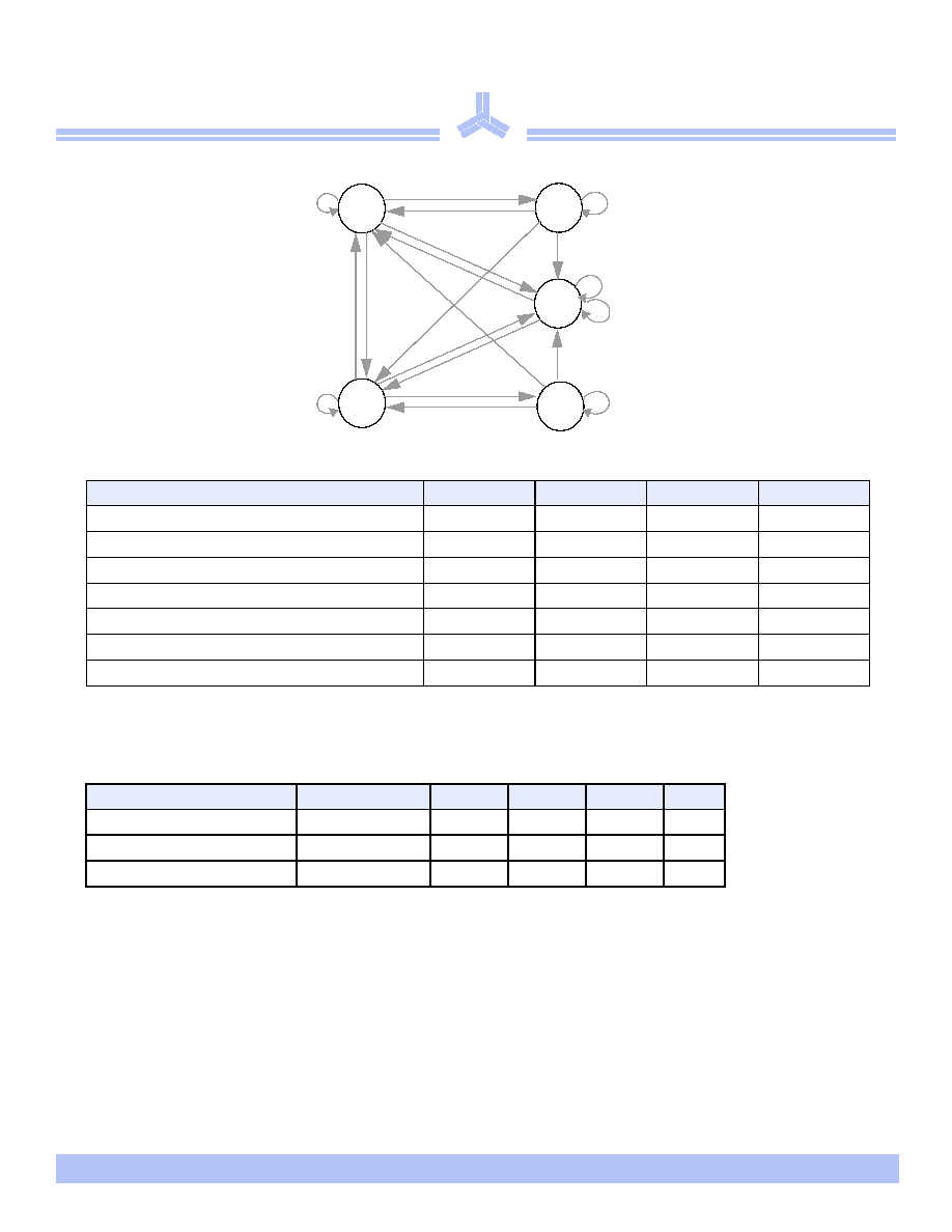
State diagram for NTD SRAM
Absolute maximum ratings
Note: Stresses greater than those listed in this table may cause permanent damage to the device. This is a stress rating only, and functional operation of the
device at these or any other conditions outside those indicated in the operational sections of this specification is not implied. Exposure to absolute maximum
rating conditions may affect reliability.
Recommended operating conditions
Parameter
Symbol
Min
Max
Unit
Power supply voltage relative to GND
V
DD
, V
DDQ
Ù0.3
+3.6
V
Input voltage relative to GND (input pins)
V
IN
Ù0.3
V
DD
+ 0.3
V
Input voltage relative to GND (I/O pins)
V
IN
Ù0.3
V
DDQ
+ 0.3
V
Power dissipation
P
d
Ù
1.8
W
Short circuit output current
I
OUT
Ù
50
mA
Storage temperature
T
stg
Ù65
+150
o
C
Temperature under bias
T
bias
Ù65 +135
o
C
Parameter
Symbol
Min
Nominal
Max
Unit
Supply voltage for inputs
V
DD
2.375
2.5
2.625
V
Supply voltage for I/O
V
DDQ
2.375
2.5
2.625
V
Ground supply
Vss
0
0
0
V
Dsel
Dsel
Rea
d
Read
Burst
Burst
Read
Writ
Burs
Read
Wr
i
t
e
Dsel
Read
Burst
Write
Ds
el
Dse
l
Wri
te
W
rit
e
Burst
Dsel
Burst
Burst
Write
Read
Û
AS7C251MNTF18A
12/23/04, v 1.1
Alliance Semiconductor
P. 8 of 18
DC electrical characteristics
LBO and ZZ pins have an internal pull-up or pull-down, and input leakage = Ý10
çA.
*
V
IH
max < VDD +1.5V for pulse width less than 0.2 X t
CYC
**
V
IL
min = -1.5 for pulse width less than 0.2 X t
CYC
I
DD
operating conditions and maximum limits
Parameter
Sym
Conditions
Min
Max
Unit
Input leakage current
|I
LI
|
V
DD
= Max, 0V < V
IN
< V
DD
-2
2
çA
Output leakage current
|I
LO
|
OE
V
IH
, V
DD
= Max, 0V < V
OUT
< V
DDQ
-2
2
çA
Input high (logic 1) voltage
V
IH
Address and control pins
1.7*
V
DD
+0.3
V
I/O pins
1.7*
V
DDQ
+0.3
V
Input low (logic 0) voltage
V
IL
Address and control pins
-0.3**
0.7
V
I/O pins
-0.3**
0.7
V
Output high voltage
V
OH
I
OH
= Ù4 mA, V
DDQ
= 2.375V
1.7
Ù
V
Output low voltage
V
OL
I
OL
= 8 mA, V
DDQ
= 2.625V
Ù
0.7
V
Parameter
Sym
Conditions
-75
-85
-10
Unit
Operating power supply current
1
1 I
CC
given with no output loading. I
CC
increases with faster cycle times and greater output loading.
I
CC
CE0 < V
IL
, CE1 > V
IH
, CE2 < V
IL
, f = f
Max
,
I
OUT
= 0 mA, ZZ
< V
IL
275
250
230
mA
Standby power supply current
I
SB
All V
IN
0.2V or > V
DD
Ù 0.2V, Deselected,
f = f
Max
, ZZ
< V
IL
90
80
80
mA
I
SB1
Deselected, f = 0, ZZ
< 0.2V,
all V
IN
0.2V or V
DD
Ù 0.2V
60
60
60
I
SB2
Deselected, f = f
Max
, ZZ
V
DD
Ù 0.2V,
all V
IN
V
IL
or
V
IH
50
50
50
Û
AS7C251MNTF18A
12/23/04, v 1.1
Alliance Semiconductor
P. 9 of 18
Timing characteristics over operating range
Snooze Mode Electrical Characteristics
Parameter
Sym
-75
-85
-10
Unit
Notes
1
1
See "Notes:" on page 15.
Min
Max
Min
Max
Min
Max
Cycle time
t
CYC
8.5
Ù
10
Ù
12
Ù
ns
Clock access time
t
CD
Ù
7.5
Ù
8.5
Ù
10
ns
Output enable low to data valid
t
OE
Ù
3.5
Ù
4.0
Ù
4.0
ns
Clock high to output low Z
t
LZC
2.5
Ù
2.5
Ù
2.5
Ù
ns
2,3,4
Data Output invalid from clock high
t
OH
3.0
Ù
3.0
Ù
3.0
Ù
ns
2
Output enable low to output low Z
t
LZOE
0
Ù
0
Ù
0
Ù
ns
2,3,4
Output enable high to output high Z
t
HZOE
Ù
3.5
Ù
4.0
Ù
4.0
ns
2,3,4
Clock high to output high Z
t
HZC
Ù
3.5
Ù
4.0
Ù
4.0
ns
2,3,4
Output enable high to invalid output
t
OHOE
0
Ù
0
Ù
0
Ù
ns
Clock high pulse width
t
CH
2.5
Ù
3.0
Ù
4.0
Ù
ns
5
Clock low pulse width
t
CL
2.5
Ù
3.0
Ù
4.0
Ù
ns
5
Address and Control setup to clock high
t
AS
2.0
Ù
2.0
Ù
2.0
Ù
ns
6
Data setup to clock high
t
DS
2.0
Ù
2.0
Ù
2.0
Ù
ns
6
Write setup to clock high
t
WS
2.0
Ù
2.0
Ù
2.0
Ù
ns
6, 7
Chip select setup to clock high
t
CSS
2.0
Ù
2.0
Ù
2.0
Ù
ns
6, 8
Address hold from clock high
t
AH
0.5
Ù
0.5
Ù
0.5
Ù
ns
6
Data hold from clock high
t
DH
0.5
Ù
0.5
Ù
0.5
Ù
ns
6
Write hold from clock high
t
WH
0.5
Ù
0.5
Ù
0.5
Ù
ns
6, 7
Chip select hold from clock high
t
CSH
0.5
Ù
0.5
Ù
0.5
Ù
ns
6, 8
Clock enable setup to clock high
t
CENS
2.0
Ù
2.0
Ù
2.0
Ù
ns
6
Clock enable hold from clock high
t
CENH
0.5
Ù
0.5
Ù
0.5
Ù
ns
6
ADV setup to clock high
t
ADVS
2.0
Ù
2.0
Ù
2.0
Ù
ns
6
ADV hold from clock high
t
ADVH
0.5
Ù
0.5
Ù
0.5
Ù
ns
6
Description
Conditions
Symbol
Min
Max
Units
Current during Snooze Mode
ZZ > V
IH
I
SB2
50
mA
ZZ active to input ignored
t
PDS
2
cycle
ZZ inactive to input sampled
t
PUS
2
cycle
ZZ active to SNOOZE current
t
ZZI
2
cycle
ZZ inactive to exit SNOOZE current
t
RZZI
0
cycle
Û
AS7C251MNTF18A
12/23/04, v 1.1
Alliance Semiconductor
P. 10 of 18
Key to switching waveforms
Timing waveform of read cycle
Undefined
Falling input
Rising input
don't care
t
CH
t
CYC
t
CL
t
AS
CLK
CEN
R/W
t
CEH
A1
A2
A3
Address
t
AH
t
CES
t
WS
t
WH
CE0,CE2
t
ADVS
t
CSH
Dout
CE1
t
ADVH
t
OE
t
LZOE
t
HZOE
Q(A1)
Q(A2Y`01)
Q(A2)
Q(A3)
t
HLZC
OE
ADV/LD
BWn
t
WS
t
WH
Q(A2Y`10)
Q(A2Y`11)
Read
Q(A1)
DSEL
Read
Q(A2)
Continue
Read
Q(A2Y`01)
Continue
Read
Q(A2Y`10)
Continue
Read
Q(A2Y`11)
Inhibit
Clock
Read
Q(A3)
Continue
Read
Q(A3Y`01)
Û
AS7C251MNTF18A
12/23/04, v 1.1
Alliance Semiconductor
P. 11 of 18
Timing waveform of write cycle
t
CH
t
CYC
t
CL
t
AS
CLK
CEN
R/W
t
CEH
A1
A2
A3
Address
t
AH
t
CES
CE0,CE2
t
ADVS
t
CSH
Din
CE1
t
ADVH
t
HZOE
D(A1)
D(A2)
D(A3)
t
DS
OE
ADV/LD
t
DH
Q(n-2)
Dout
BWn
Q(n-1)
D(A2Y`01)
D(A2Y`10) D(A2Y`11)
Write
D(A1)
DSEL
Write
D(A2)
Continue
Write
D(A2Y`01)
Continue
Write
D(A2Y`10)
Continue
Write
D(A2Y`11)
Inhibit
Clock
Write
D(A3)
Continue
Write
D(A3Y`01)
Û
AS7C251MNTF18A
12/23/04, v 1.1
Alliance Semiconductor
P. 12 of 18
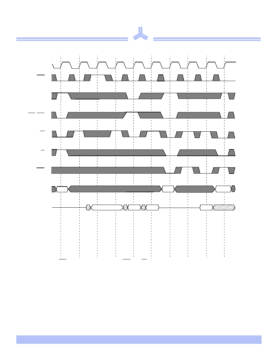
Timing waveform of read/write cycle
Note: ï = XOR when LBO = high/no connect. ï = ADD when LBO = low. BW[a:d] is don't care.
t
CH
t
CYC
t
CL
t
CENS
t
OH
t
OE
CLK
CEN
CE0, CE2
ADV/LD
R/W
ADDRESS
D/Q
OE
Command
t
HZOE
BWn
A2
A1
A3
A5
A4
A7
A6
D(A1)
D(A5)
Q(A6)
D(A2)
D(A2ï01)
Q(A3)
Q(A4)
Q(A4ï01)
t
CENH
t
DS
t
DH
t
LZC
t
CD
t
HZC
t
LZOE
Read
Q(A3)
Read
Q(A4)
Burst
Read
Q(A4ï01)
Write
D(A5)
Read
Q(A6)
Write
D(A7)
DSEL
t
CSS
t
ADVH
t
WS
t
WH
t
WS
t
WH
CE1
Write
D(A1)
Write
D(A2)
t
ADVS
t
CSH
t
AS
t
AH
Burst
Write
D(A2ï01)
Û
AS7C251MNTF18A
12/23/04, v 1.1
Alliance Semiconductor
P. 13 of 18
NOP, stall and deselect cycles
Note: ï = XOR when LBO = high/no connect; ï = ADD when LBO = low. OE is low.
CLK
CEN
CE0, CE2
ADV/LD
R/W
Address
D/Q
Command
BWn
A1
A2
Q(A1)
D(A2)
Q(A1ï01)
Q(A1ï10)
Burst
Q(A1ï01)
STALL
DSEL
Burst
DSEL
Write
D(A2)
Burst
NOP
D(A2ï01)
Write
NOP
D(A3)
A3
Read
Q(A1)
Burst
Q(A1ï10)
Burst
D(A2ï10)
CE1
Û
AS7C251MNTF18A
12/23/04, v 1.1
Alliance Semiconductor
P. 14 of 18
Timing waveform of snooze mode
CLK
All inputs
ZZ
t
ZZI
I
supply
(except ZZ)
Dout
t
PUS
ZZ recovery cycle
I
SB2
t
RZZI
ZZ setup cycle
Deselect or Read Only
Deselect or Read Only
Normal
operation
Cycle
High-Z
Û
AS7C251MNTF18A
12/23/04, v 1.1
Alliance Semiconductor
P. 15 of 18
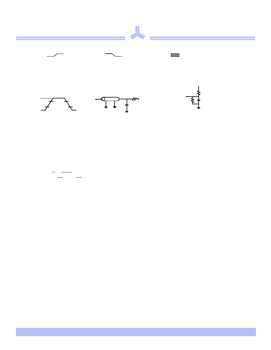
AC test conditions
Notes:
1) For test conditions, see "AC test conditions", Figures A, B, C
2) This parameter measured with output load condition in Figure C.
3) This parameter is sampled, but not 100% tested.
4) t
HZOE
is less than t
LZOE
and t
HZC
is less than t
LZC
at any given temperature and voltage.
5) t
CH
measured high above V
IH
and t
CL
measured as low below V
IL
6) This is a synchronous device. All addresses must meet the specified setup and hold times for all rising edges of CLK. All other synchronous inputs must
meet the setup and hold times with stable logic levels for all rising edges of CLK when chip is enabled.
7) Write refers to
R/W and BW[a,b]
.
8) Chip select refers to
CE0, CE1, and CE2
.
Undefined/don't care
Falling input
Rising input
ñ Output load: For t
LZC
, t
LZOE
, t
HZOE
, and t
HZC
, see Figure C. For all others, see Figure B.
ñ Input pulse level: GND to 2.5V. See Figure A.
ñ Input rise and fall time (measured at 0.25V and 2.25V): 2 ns. See Figure A.
ñ Input and output timing reference levels: 1.25V.
D
OUT
50
Figure B: Output load (A)
30 pF*
Figure A: Input waveform
10%
90%
GND
90%
10%
+2.5V
V
L
= V
DDQ
/2
Thevenin equivalent:
353
/1538
5 pF*
319
/1667
D
OUT
GND
Figure C: Output load(B)
*including scope
and jig capacitance
+2.5V
Û
AS7C251MNTF18A
12/23/04, v 1.1
Alliance Semiconductor
P. 16 of 18
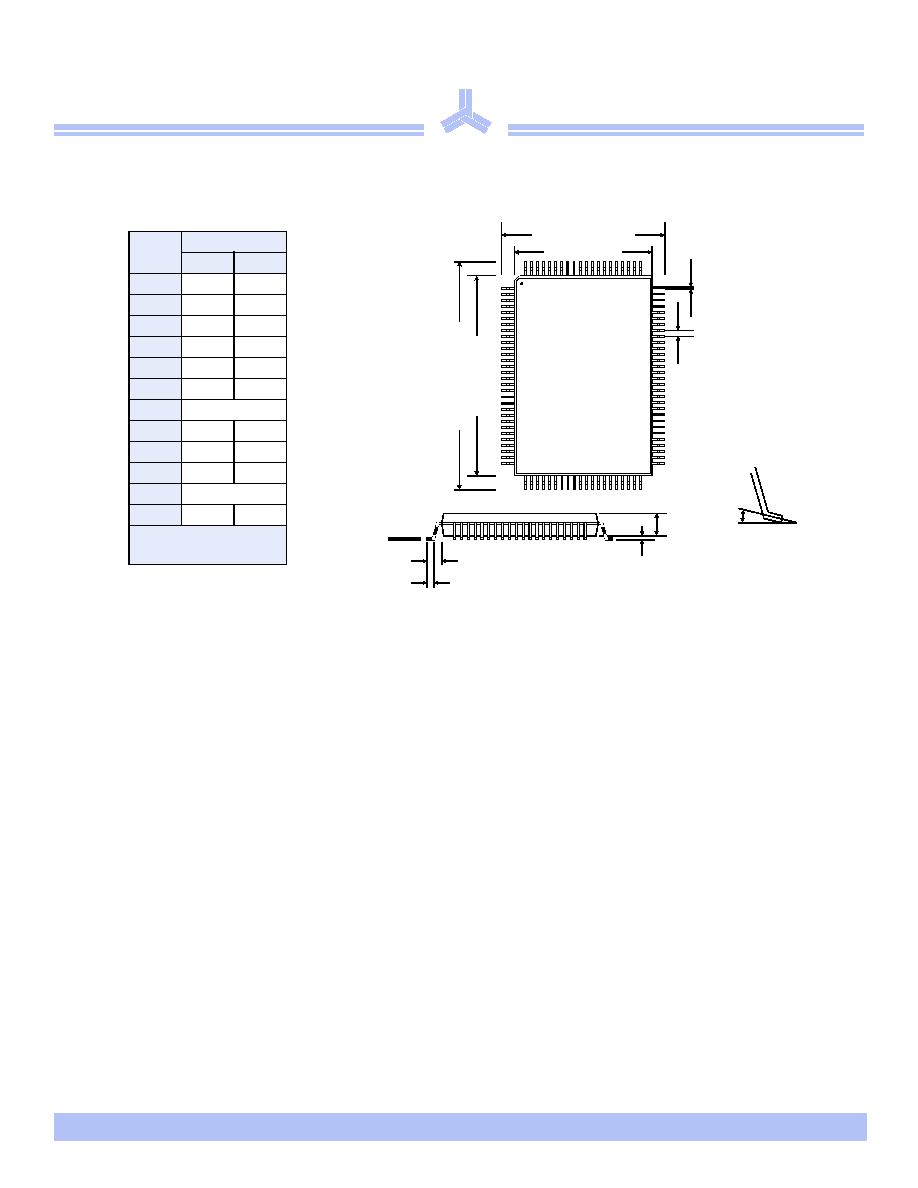
Package dimensions
100-pin quad flat pack (TQFP)
TQFP
Min
Max
A1
0.05
0.15
A2
1.35
1.45
b
0.22
0.38
c
0.09
0.20
D
13.90
14.10
E
19.90
20.10
e
0.65 nominal
Hd
15.85
16.15
He
21.80
22.20
L
0.45
0.75
L1
1.00 nominal
0¯
7¯
Dimensions in
millimeters
A1 A2
L1
L
c
He E
Hd
D
b
e
Û
AS7C251MNTF18A
12/23/04, v 1.1
Alliance Semiconductor
P. 17 of 18
Ordering information
Note: Add suffix `N' to the above part numbers for Lead Free Parts (Ex. AS7C251MNTF18A-85TQCN)
Part numbering guide
1. Alliance Semiconductor SRAM prefix
2. Operating voltage: 25 = 2.5V
3. Organization: 1M
4. NTF = No Turn-Around Delay. Flow-through mode
5. Organization: 18 = x 18
6. Production version: A = first production version
7. Clock access time: [-75 = 7.5 ns access time; -85 = 8.5 ns access time; -10 = 10.0 ns access time]
8. Package type: TQ = TQFP
9. Operating temperature: C = commercial (
0
¯ C to 70¯ C); I = industrial (-40¯ C to 85¯ C)
10. N = Lead free part
Package
&Width
Ù75
Ù85
Ù10
TQFP x18
AS7C251MNTF18A-75TQC
AS7C251MNTF18A-85TQC
AS7C251MNTF18A-10TQC
AS7C251MNTF18A-75TQI
AS7C251MNTF18A-85TQI
AS7C251MNTF18A-10TQI
AS7C
25
1M
NTF
18
A
ÙXX
TQ
C/I
X
1
2
3
4
5
6
7
8
9
10

Û
AS7C251MNTF18A
ˋ Copyright 2003 Alliance Semiconductor Corporation. All rights reserved. Our three-point logo, our name and Intelliwatt are
trademarks or registered trademarks of Alliance. All other brand and product names may be the trademarks of their respective
companies. Alliance reserves the right to make changes to this document and its products at any time without notice. Alliance assumes
no responsibility for any errors that may appear in this document. The data contained herein represents Alliance's best data and/or
estimates at the time of issuance. Alliance reserves the right to change or correct this data at any time, without notice. If the product
described herein is under development, significant changes to these specifications are possible. The information in this product data
sheet is intended to be general descriptive information for potential customers and users, and is not intended to operate as, or provide,
any guarantee or warrantee to any user or customer. Alliance does not assume any responsibility or liability arising out of the
application or use of any product described herein, and disclaims any express or implied warranties related to the sale and/or use of
Alliance products including liability or warranties related to fitness for a particular purpose, merchantability, or infringement of any
intellectual property rights, except as express agreed to in Alliance's Terms and Conditions of Sale (which are available from
Alliance). All sales of Alliance products are made exclusively according to Alliance's Terms and Conditions of Sale. The purchase of
products from Alliance does not convey a license under any patent rights, copyrights; mask works rights, trademarks, or any other
intellectual property rights of Alliance or third parties. Alliance does not authorize its products for use as critical components in life-
supporting systems where a malfunction or failure may reasonably be expected to result in significant injury to the user, and the
inclusion of Alliance products in such life-supporting systems implies that the manufacturer assumes all risk of such use and agrees to
indemnify Alliance against all claims arising from such use.
Alliance Semiconductor Corporation
2575, Augustine Drive,
Santa Clara, CA 95054
Tel: 408 - 855 - 4900
Fax: 408 - 855 - 4999
www.alsc.com
Copyright ˋ Alliance Semiconductor
All Rights Reserved
Part Number: AS7C251MNTF18A
Document Version: v 1.1
Û