Copyright ę Alliance Semiconductor. All rights reserved.
AS4C256K16FO
4/11/01; V.0.9.1
Alliance Semiconductor
P. 1 of 25
5V 256K X 16 CMOS DRAM (Fast Page Mode)
«
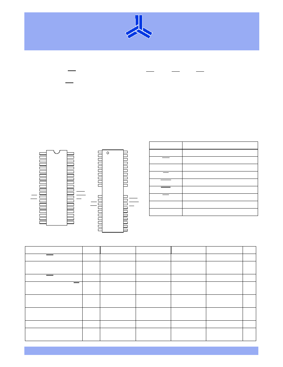
Pin designation
Pin(s)
Description
A0 to A8
Address inputs
RAS
Row address strobe
I/O0 to I/O15
Input/output
OE
Output enable
UCAS
Column address strobe, upper byte
LCAS
Column address strobe, lower byte
WE
Read/write control
V
CC
Power (+5V
▒
10%)
GND
Ground
Features
Ě Organization: 262,144 words Î 16 bits
Ě High speed
- 25/30/35/50 ns RAS access time
- 12/16/18/25 ns column address access time
- 7/10/10/10 ns CAS access time
Ě Low power consumption
- Active: 770 mW max (ASAS4C256K16FO-50)
- Standby: 5.5 mW max, CMOS I/O
Ě Fast page mode
Ě AS4C256K16FO-50 timings
are also valid for
AS4C256K16FO-60.
Ě Refresh
- 512 refresh cycles, 8 ms refresh interval
- RAS-only or CAS-before-RAS refresh or self-refresh
- Self-refresh option is available for new generation
device only. Contact Alliance for more information.
Ě Read-modify-write
Ě TTL-compatible, three-state I/O
Ě JEDEC standard packages
- 400 mil, 40-pin SOJ
- 400 mil, 40/44-pin TSOP II
Ě Single 5V power supply/built-in V
bb
generator
Ě Latch-up current > 200 mA
Pin arrangement
40
39
38
37
36
35
34
33
32
31
GND
I/O15
I/O14
I/O13
I/O12
GND
I/O11
I/O10
I/O9
I/O8
SOJ
30
29
28
27
26
25
24
23
22
21
NC
LCAS
UCAS
OE
A8
A7
A6
A5
A4
GND
1
2
3
4
5
6
7
8
9
10
V
CC
I/O0
I/O1
I/O2
I/O3
V
CC
I/O4
I/O5
I/O6
I/O7
11
12
13
14
15
16
17
18
19
20
NC
NC
WE
RAS
NC
A0
A1
A2
A3
V
CC
V
CC
I/O0
I/O1
I/O2
I/O3
V
CC
I/O4
I/O5
I/O6
I/O7
NC
NC
WE
RAS
NC
A0
A1
A2
A3
V
CC
V
SS
I/O15
I/O14
I/O13
I/O12
V
SS
I/O11
I/O10
I/O9
I/O8
NC
LCAS
UCAS
OE
A8
A7
A6
A5
A4
V
SS
44
43
42
41
40
39
38
37
36
35
32
31
30
29
28
27
26
25
24
23
1
2
3
4
5
6
7
8
9
10
13
14
15
16
17
18
19
20
21
22
TSOP II
A
S
C
2
56
K1
6F
O
A
S
C2
56
K1
6F
O
Selection guide
Symbol
ş25
ş30
ş35
ş50
Unit
Maximum RAS access time
t
RAC
25
30
35
50
ns
Maximum column address
access time
t
CAA
12
16
18
25
ns
Maximum CAS access time
t
CAC
7
10
10
10
ns
Maximum output enable (OE)
access time
t
OEA
7
10
10
10
ns
Minimum read or write cycle
time
t
RC
40
65
70
85
ns
Minimum EDO page mode
cycle time
t
PC
12
12
14
25
ns
Maximum operating current
I
CC1
200
180
160
140
mA
Maximum CMOS standby
current
I
CC2
2.0
2.0
2.0
2.0
mA
«
AS4C256K16FO
4/11/01; V.0.9.1
Alliance Semiconductor
P. 2 of 25
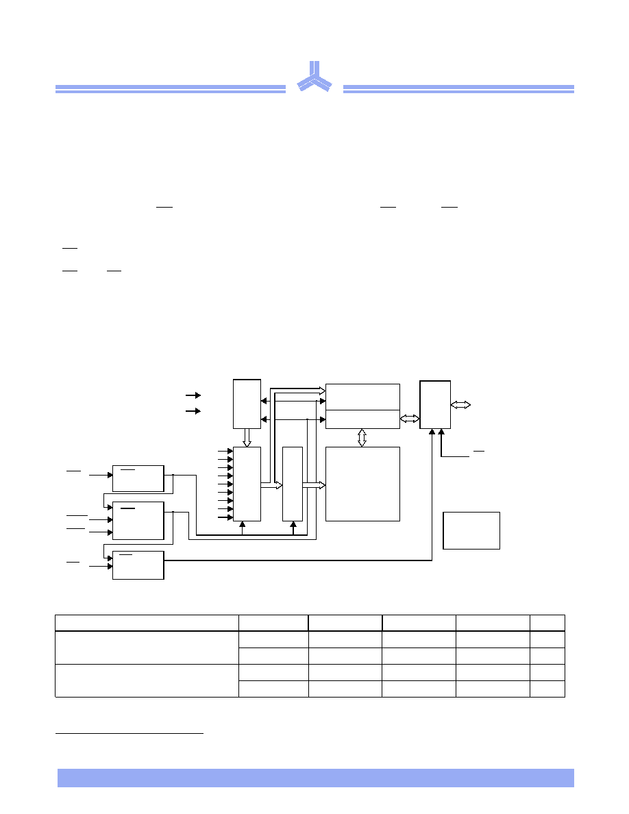
Functional description
The AS4C256K16FO is a high-performance 4 megabit CMOS Dynamic Random Access Memory (DRAM) device organized as
262,144 words Î 16 bits. The AS4C256K16FO is fabricated with advanced CMOS technology and designed with innovative
design techniques resulting in high speed, extremely low power and wide operating margins at component and system levels.
The AS4C256K16FO features a high-speed page mode operation in which high speed read, write and read-write are performed
on any of the 512
Î
16 bits defined by the column address. The asynchronous column address uses an extremely short row
address capture time to ease the system-level timing constraints associated with multiplexed addressing. Output is tri-stated by a
column address strobe (CAS) which acts as an output enable independent of RAS. Very fast CAS to output access time eases
system design.
Refresh on the 512 address combinations of A0şA8 during an 8 ms period is accomplished by performing any of the following:
Ě RAS-only refresh cycles
Ě Hidden refresh cycles
Ě CAS-before-RAS refresh cycles
Ě Normal read or write cycles
Ě Self-refresh cycles.
*
The AS4C256K16FO is available in standard 40-pin plastic SOJ and 44-pin TSOP II packages compatible with widely available
automated testing and insertion equipment. System level features include single power supply of 5V ▒ 10% tolerance and direct
interface with TTL logic families.
Logic block diagram
Recommended operating conditions
* Self-refresh option is available for new generation device only. Contact Alliance for more information.
Parameter
Symbol
Min
Typ
Max
Unit
Supply voltage
V
CC
4.5
5.0
5.5
V
GND
0.0
0.0
0.0
V
Input voltage
V
IH
2.4
ş
V
CC
+ 1
V
V
IL
ş1.0
ş
0.8
V
512
Î
512
Î
16
array
(4,194,304)
Sense amp
A0
A1
A2
A3
A4
A5
A6
A7
V
CC
GND
A
d
dre
e
s
s
bu
f
f
e
r
s
A8
Ro
w deco
der
Column decoder
OE
RAS
UCAS
WE
LCAS
I/O0 to I/O15
Substrate
bias generator
Data
I/O
buffer
Re
fr
es
h
con
t
r
o
l
l
e
r
RAS clock
generator
CAS clock
generator
WE clock
generator

«
AS4C256K16FO
4/11/01; V.0.9.1
Alliance Semiconductor
P. 3 of 25
Absolute maximum ratings
Note: Stresses greater than those listed under Absolute Maximum Ratings may cause permanent damage to the device. This is a stress rating only and functional
operation of the device at these or any other conditions outside those indicated in the operational sections of this specification is not implied. Exposure to
absolute maximum rating conditions for extended periods may affect reliability.
DC electrical characteristics
(V
CC
= 5 ▒ 10%, GND = 0V, T
a
= 0
░
C to +70
░
C)
Parameter
Symbol
Min
Max
Unit
Input voltage
V
IN
ş1.0
+7.0
V
Output voltage
V
OUT
ş1.0
+7.0
V
Power supply voltage
V
CC
ş1.0
+7.0
V
Operating temperature
T
OPR
0
+70
░C
Storage temperature (plastic)
T
STG
ş55
+150
░C
Soldering temperature
Î
time
T
SOLDER
ş
260
Î
10
░
C
Î
sec
Power dissipation
P
D
ş
1
W
Short circuit output current
I
OUT
ş
50
mA
Latch-up current
200
ş
mA
Parameter
Symbol
Test conditions
ş25
ş30
ş35
ş50
Unit Note
Min
Max
Min
Max
Min
Max
Min
Max
Input leakage
current
I
IL
0V
V
IN
+ 5.5V
pins not under test = 0V
ş10
10
ş10
10
ş10
10
ş10
10
Á
A
Output leakage
current
I
OL
D
OUT
disabled,
0V
V
OUT
+ 5.5V
ş10
10
ş10
10
ş10
10
ş10
10
Á
A
Operating
power supply
current
I
CC1
RAS, UCAS, LCAS, address
cycling; t
RC
= min
ş
200
ş
180
ş
160
ş
140
mA
1,2
TTL standby
power supply
current
I
CC2
RAS = UCAS = LCAS = VIH
ş
2.0
ş
2.0
ş
2.0
ş
2.0
mA
Average power
supply current,
RAS refresh
mode
I
CC3
RAS cycling,
UCAS = LCAS = V
IH
,
t
RC
= min
ş
120
ş
200
ş
190
ş
140
mA
1
Fast page mode
average power
supply current
I
CC4
RAS = UCAS = LCAS = V
IL
,
address cycling: t
SC
= min
ş
130
ş
190
ş
180
ş
70
mA
1,2
CMOS standby
power supply
current
I
CC5
RAS = UCAS = LCAS =
V
CC
ş 0.2V
ş
0.60
ş
1.0
ş
1.0
ş
1.0
mA
CAS-before-RAS
refresh power
supply current
I
CC6
RAS, UCAS, LCAS, cycling;
t
RC
= min
ş
120
ş
200
ş
190
ş
140
mA
1
Output voltage
V
OH
I
OUT
= ş 5.0 mA
2.4
ş
2.4
ş
2.4
ş
2.4
ş
V
V
OL
I
OUT
= 4.2 mA
ş
0.4
ş
0.4
ş
0.4
ş
0.4
V
Self refresh
current
I
CC7
RAS = UCAS = LCAS = V
IL
, WE
= OE = A0 ş A8 = V
CC
ş0.2V,
DQ0 ş DQ15 = V
CC
ş 0.2V, 0.2V
are open
ş
2.0
ş
2.0
ş
2.0
ş
2.0
mA
«
AS4C256K16FO
4/11/01; V.0.9.1
Alliance Semiconductor
P. 4 of 25
AC parameters common to all waveforms
(V
CC
= 5V ▒ 10%, GND = 0V, T
a
= 0
░
C to +70
░
C)
Read cycle
(V
CC
= 5V▒10%, GND = 0V, T
a
= 0
░
C to + 70
░
C)
Standard
Symbol
Parameter
ş25
ş30
ş35
ş50
Unit
Notes
Min
Max
Min
Max
Min
Max
Min
Max
t
RC
Random read or write cycle time
45
ş
65
ş
70
ş
85
ş
ns
t
RP
RAS precharge time
15
ş
25
ş
25
ş
25
ş
ns
t
RAS
RAS pulse width
25
75K
30
75K
35
75K
50
75K
ns
t
CAS
CAS pulse width
4
ş
5
ş
6
ş
10
ş
ns
t
RCD
RAS to CAS delay time
10
17
15
20
16
24
15
35
ns
6
t
RAD
RAS to column address delay time
8
13
10
14
11
17
15
25
ns
7
t
RSH(R)
CAS to RAS hold time (read cycle)
7
ş
10
ş
10
ş
10
ş
ns
t
CSH
RAS to CAS hold time
20
ş
30
ş
35
ş
50
ş
ns
t
CRP
CAS to RAS precharge time
5
ş
5
ş
5
ş
5
ş
ns
t
ASR
Row address setup time
0
ş
0
ş
0
ş
0
ş
ns
t
RAH
Row address hold time
5
ş
5
ş
6
ş
9
ş
ns
t
T
Transition time (rise and fall)
1.5
50
1.5
50
1.5
50
3
50
ns
4,5
t
REF
Refresh period
ş
8
ş
8
ş
8
ş
8
ms
3
t
CLZ
CAS to output in low Z
0
ş
0
ş
0
ş
3
ş
ns
8
Standard
Symbol
Parameter
ş25
ş30
ş35
ş50
Unit
Notes
Min
Max
Min
Max
Min
Max
Min
Max
t
RAC
Access time from RAS
ş
25
ş
30
ş
35
ş
50
ns
6
t
CAC
Access time from CAS
ş
7
ş
10
ş
10
ş
10
ns
6,13
t
AA
Access time from address
ş
12
ş
16
ş
18
ş
25
ns
7,13
t
AR(R)
Column add hold from RAS
19
ş
26
ş
28
ş
30
ş
ns
t
RCS
Read command setup time
0
ş
0
ş
0
ş
0
ş
ns
t
RCH
Read command hold time to CAS
0
ş
0
ş
0
ş
0
ş
ns
9
t
RRH
Read command hold time to RAS
0
ş
0
ş
0
ş
0
ş
ns
9
t
RAL
Column address to RAS Lead time
12
ş
16
ş
18
ş
25
ş
ns
t
CPN
CAS precharge time
4
ş
3
ş
4
ş
5
ş
ns
t
OFF
Output buffer turn-off time
0
6
0
8
0
8
0
8
ns
8,10
«
AS4C256K16FO
4/11/01; V.0.9.1
Alliance Semiconductor
P. 5 of 25
Write cycle
(V
CC
= 5V ▒ 10%, GND = 0V, T
a
= 0
░
C to +70
░
C)
Read-modify-write cycle
(V
CC
= 5V ▒ 10%, GND = 0V, T
a
= 0
░
C to +70
░
C)
Fast page mode cycle
(V
CC
= 5V ▒ 10%, GND = 0V, T
a
= 0
░
C to +70
░
C)
Standard
Symbol
Parameter
ş25
ş30
ş35
ş50
Unit
Notes
Min
Max
Min
Max
Min
Max
Min
Max
t
ASC
Column address setup time
0
ş
0
ş
0
ş
0
ş
ns
t
CAH
Column address hold time
5
ş
5
ş
5
ş
9
ş
ns
t
AWR
Column address hold time to RAS
19
ş
26
ş
28
ş
30
ş
ns
t
WCS
Write command setup time
0
ş
0
ş
0
ş
0
ş
ns
11
t
WCH
Write command hold time
5
ş
5
ş
5
ş
9
ş
ns
11
t
WCR
Write command hold time to RAS
19
ş
26
ş
28
ş
30
ş
ns
t
WP
Write command pulse width
5
ş
5
ş
5
ş
9
ş
ns
t
RWL
Write command to RAS lead time
7
ş
10
ş
11
ş
12
ş
ns
t
CWL
Write command to CAS lead time
5
ş
10
ş
11
ş
12
ş
ns
t
DS
Data-in setup time
0
ş
0
ş
0
ş
0
ş
ns
12
t
DH
Data-in hold time
5
ş
5
ş
5
ş
9
ş
ns
12
t
DHR
Data-in hold time to RAS
19
ş
26
ş
28
ş
30
ş
ns
Standard
Symbol
Parameter
ş25
ş30
ş35
ş50
Unit
Notes
Min
Max
Min
Max
Min
Max
Min
Max
t
RWC
Read-write cycle time
100
ş
100
ş
105
ş
120
ş
ns
t
RWD
RAS to WE delay time
34
ş
50
ş
54
ş
60
ş
ns
11
t
CWD
CAS to WE delay time
17
ş
26
ş
28
ş
30
ş
ns
11
t
AWD
Column address to WE delay time
21
ş
32
ş
35
ş
40
ş
ns
11
t
RSH(W)
CAS to RAS hold time (write)
7
ş
10
ş
10
ş
12
ş
ns
t
CAS(W)
CAS pulse width (write)
15
ş
15
ş
15
ş
15
ş
ns
Standard
Symbol
Parameter
ş25
ş30
ş35
ş50
Unit
Notes
Min
Max
Min
Max
Min
Max
Min
Max
t
PC
Read or write cycle time
8
ş
12
ş
14
ş
25
ş
ns
14
t
CAP
Access time from CAS precharge
ş
14
ş
19
ş
21
ş
23
ns
13
t
CP
CAS precharge time
3
ş
3
ş
4
ş
5
ş
ns
t
PCM
Fast page mode RMW cycle
56
ş
56
ş
58
ş
60
ş
ns
t
CRW
Page mode CAS pulse width (RMW)
44
ş
44
ş
46
ş
50
ş
ns
t
RASP
RAS pulse width
25
75K
30
75K
35
75K
50
75K
ns