
Alpha Industries, Inc. [781] 935-5150
· Fax [617] 824-4579 · Email sales@alphaind.com · www.alphaind.com
1
Specifications subject to change without notice. 6/01A
HIP3TM Variable Attenuator
1.702.00 GHz
Features
I +50 dBm IP3 Typical
I Low Loss 1 dB Typical
I Attenuation 30 dB Typical
I Good VSWR <1.5:1 Typical
I Small SOIC-8 Package
AV102-12
Description
The AV102-12 is a current controlled variable attenuator
from Alpha's series of HIP3TM components. It is designed
to meet the wide dynamic range required in spread
spectrum wireless base station applications. A monolithic
quadrature hybrid is teamed with a silicon PIN diode pair
in a plastic surface mount package reducing size and
assuring consistency from part to part.
Parameter
Min.
Typ.
Max.
Unit
Frequency
1.70
2.00
GHz
Insertion Loss (0 mA Control Current)
1
1.5
dB
Attenuation @ 3.0 mA Control Current (1850 MHz)
18.5
25.0
dB
VSWR All Ports
1.5
1.8
Input 3rd Order Intercept
+47
+50
dBm
Group Delay
0.6
1.0
ns
Electrical Specifications at 25°C
Parameter
1
Condition
Frequency
Min.
Typ.
Max.
Unit
Switching Characteristics
2
Rise, Fall (10/90% or 90/10% RF)
5
µs
On, Off (50% CTL to 90/10% RF)
8
µs
Video Feedthru (Peak)
2
mV
Maximum Input Power for <1 dB
Attenuation Variation
+15
dBm
Operating Characteristics at 25°C (0, +5 V)
1. All measurements made in a 50
system, unless otherwise specified.
2. 04 mA square wave total control current.
2
Alpha Industries, Inc. [781] 935-5150
· Fax [617] 824-4579 · Email sales@alphaind.com · www.alphaind.com
Specifications subject to change without notice. 6/01A
HIP3TM Variable Attenuator 1.702.00 GHz
AV102-12
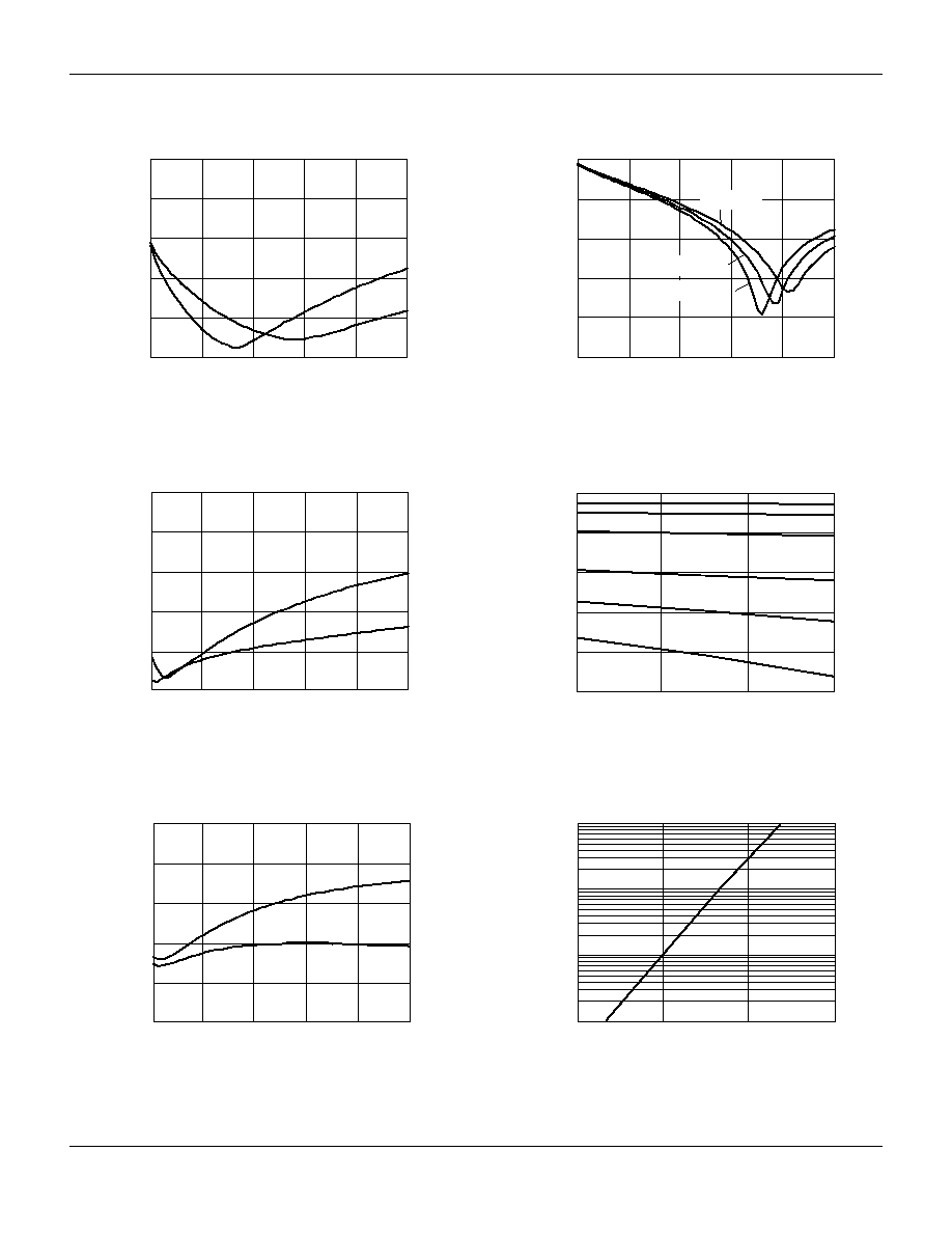
VSWR (:1)
Input/Output VSWR vs. Current
@ 1700 MHz
1.0
1.1
1.2
1.3
1.4
1.5
0.0000
0.0010
0.0020
0.0030
0.0040
0.0050
Current (Amps)
Input
Output
VSWR (:1)
Input/Output VSWR vs. Current
@ 1850 MHz
1.0
1.1
1.2
1.3
1.4
1.5
Current (Amps)
0.0000
0.0010
0.0020
0.0030
0.0040
0.0050
Input
Output
Atten
uation (dB)
0.0000
0.0010
0.0020
0.0030
0.0040
0.0050
Attenuation vs. Current
-50.0
-40.0
-30.0
-20.0
-10.0
0.0
Current (Amps)
1850 MHz
2000 MHz
1700 MHz
Atten
uation (dB)
1.70
1.80
1.90
2.00
Attenuation vs. Frequency
-25.0
-20.0
-15.0
-10.0
-5.0
0.0
Frequency (GHz)
0.0 mA
0.2 mA
0.7 mA
1.7 mA
2.4 mA
3.0 mA
Input/Output VSWR vs. Current
@ 2000 MHz
1.0
1.1
1.2
1.3
1.4
1.5
Current (Amps)
VSWR (:1)
0.0000
0.0010
0.0020
0.0030
0.0040
0.0050
Input
Output
Diode Current (mA)
400
600
800
1000
Typical PIN Diode Current vs. Voltage
0.01
0.1
1
10
Diode Voltage (mV)
Typical Performance Data
HIP3TM Variable Attenuator 1.702.00 GHz
AV102-12
Alpha Industries, Inc. [781] 935-5150
· Fax [617] 824-4579 · Email sales@alphaind.com · www.alphaind.com
3
Specifications subject to change without notice. 6/01A
Characteristic
Value
RF Input Power
.5 W CW, 4 W @ 12.5%
Duty Cycle
Control Current
50 mA Each Diode
Operating Temperature
-40 to +85°C
Storage Temperature
-40 to +85°C
Maximum Reverse Diode Voltage
-10 V
Electrostatic Discharge
+125 V
Absolute Maximum Ratings
Note: Operating this device above any of these parameters may cause
irreversible damage.
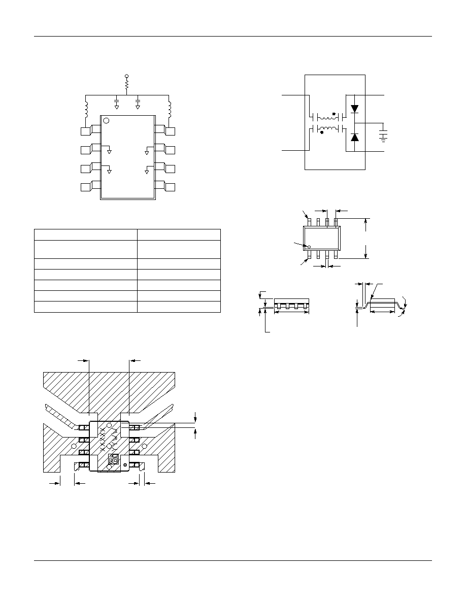
Recommended Board Layout
0.1630
0.0200 DIA.
VIA 4 PLACES
0.0190 TYP.
0.0555 TYP.
SOIC-8
0.049
(1.24 mm)
0.016
(0.41 mm)
0.016 MAX.
(0.41 mm) x
45° CHAMFER
PIN 1
0.197 (5.00 mm)
0.189 (4.80 mm)
0.068
(1.73 mm) MAX.
0.010 (0.25 mm)
0.004 (0.10 mm)
0.010 (0.25 mm)
0.007 (0.17 mm)
0.158 (4.00 mm)
0.150 (3.80 mm)
8°
MAX.
0.020 (0.51 mm) MAX.
0.244 (6.20 mm)
0.228 (5.80 mm)
0.050 (1.27 mm) BSC
PIN 8
PIN 1
INDICATOR
12
3
4
CONTROL
CURRENT
GND
220 pF
RF In
GND
680
87
6
5
GND
220 pF
100 nH
100 nH
RF Out
CONTROL
CURRENT
GND
Pin Out
CONTROL
CURRENT
CONTROL
CURRENT
RF OUT
RF IN
Connection Diagram
Material is 10 mil FR4.